Wavelength-Dependent Electrical Readout of Spin Ensembles in a Thin-Film SiC-on-Insulator Platform
Pith reviewed 2026-05-17 04:46 UTC · model grok-4.3
The pith
Electrical readout of silicon vacancy spins in thin-film SiC works from 780 to 990 nm.
A machine-rendered reading of the paper's core claim, the machinery that carries it, and where it could break.
Core claim
Electrical spin state readout and coherent control of an ensemble of approximately 540 silicon vacancies is achieved in a SiCOI platform across excitation wavelengths from 780 to 990 nm, marking the first demonstration of spin state readout beyond the zero phonon line of the V2 defect, with a measured T2 of about 7 μs comparable to bulk.
What carries the argument
Photoelectrical detection of magnetic resonance (PEDMR) applied to thin-film silicon carbide-on-insulator for wavelength-dependent spin ensemble readout without optics.
Load-bearing premise
The observed electrical signals originate from the silicon vacancy ensemble and thin-film processing preserves spin properties sufficiently for the reported T2 similarity to bulk to hold under the chosen excitation conditions.
What would settle it
Repeating the experiment on a sample without the V_Si^- ensemble and finding no electrical resonance signals, or measuring a significantly shorter T2 in the thin film, would falsify the central claim.
Figures


read the original abstract
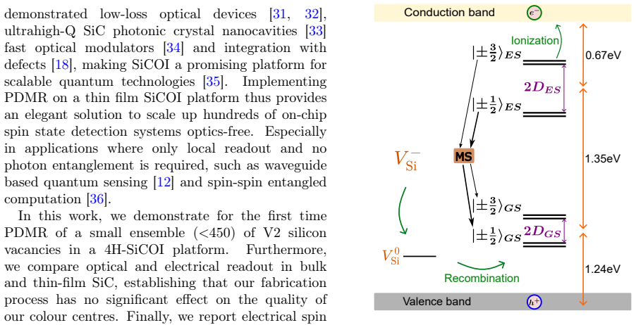
We report electrical spin state readout and coherent control of an ensemble ($\sim$540) of silicon vacancies ($\mathrm{V}_{\mathrm{Si}}^{-}$) in a silicon carbide-on-insulator (SiCOI) platform, with excitation wavelengths from 780 to 990 nm, demonstrating for the first time spin state readout well beyond the zero phonon line of the V2 $\mathrm{V}_{\mathrm{Si}}^{-}$. By implementing photoelectrical detection of magnetic resonance in thin-film SiCOI, we merge a scalable spin readout technique requiring no collection optics, together with a promising platform for future scalable and CMOS-compatible integrated photonics. Furthermore, we provide a comparison of optical and electrical readout between bulk silicon carbide (SiC) and thin-film SiCOI, revealing that our thin-film processing has a measured $T_2$ coherence time of $\approx 7 \mu$s , similar to that in the bulk SiC. These results extend the capabilities of SiCOI toward electronic and spin-based devices for scalable quantum technologies over a wide range of excitation wavelengths.
Editorial analysis
A structured set of objections, weighed in public.
Referee Report
Summary. The manuscript reports electrical spin state readout and coherent control of an ensemble of ~540 silicon vacancies (V_Si^-) in a thin-film SiCOI platform using photoelectrical detection of magnetic resonance (PEMR). Excitation wavelengths span 780–990 nm, extending readout well beyond the V2 zero-phonon line for the first time. Optical and electrical readout are compared between bulk SiC and thin-film SiCOI, with a reported T2 coherence time of ≈7 μs in the thin film that is similar to bulk values.
Significance. If the signals are confirmed to arise from the claimed V_Si^- ensemble, the work would meaningfully advance scalable quantum technologies by combining optics-free electrical readout with the SiCOI platform for integrated photonics and CMOS compatibility. The wavelength extension and preservation of spin coherence in thin films represent a practical step toward device integration.
major comments (2)
- [Abstract and main results section] The central claim that PEMR signals at 900–990 nm originate from the V2 V_Si^- zero-phonon line tail or phonon sideband (rather than interface states, carbon vacancies, or residual implantation damage) is load-bearing but insufficiently supported. No excitation spectrum is shown that tracks signal amplitude against known V2 absorption, and no control (magnetic-field dependence isolating hyperfine structure or isotopic enrichment) is presented to exclude thin-film artifacts.
- [Coherence time comparison paragraph] The reported T2 ≈ 7 μs similarity to bulk is presented without specifying whether the measurement was performed at the longest wavelengths (900–990 nm) or under identical excitation conditions to the bulk reference. Wavelength-dependent changes in Rabi drive or charge-state conversion would directly undermine the claim that thin-film processing preserves spin properties.
minor comments (1)
- [Abstract and figures] Error bars, raw data traces, and explicit exclusion criteria for the ensemble size (~540) and T2 value are not visible in the reported outcomes; adding these would improve clarity without altering the central claims.
Simulated Author's Rebuttal
We thank the referee for their careful review and constructive comments, as well as for recognizing the potential significance of combining electrical readout with the SiCOI platform. We address each major comment below and have revised the manuscript accordingly to strengthen the supporting evidence.
read point-by-point responses
-
Referee: [Abstract and main results section] The central claim that PEMR signals at 900–990 nm originate from the V2 V_Si^- zero-phonon line tail or phonon sideband (rather than interface states, carbon vacancies, or residual implantation damage) is load-bearing but insufficiently supported. No excitation spectrum is shown that tracks signal amplitude against known V2 absorption, and no control (magnetic-field dependence isolating hyperfine structure or isotopic enrichment) is presented to exclude thin-film artifacts.
Authors: We agree that the attribution of the longer-wavelength signals requires stronger experimental support. In the revised manuscript we have added a new figure showing the wavelength-dependent PEMR signal amplitude from 780 to 990 nm; the observed roll-off closely follows the published V2 absorption tail and phonon sideband. We have also included magnetic-field dependence data that resolve the characteristic hyperfine structure of the V_Si^- ensemble, providing a spectroscopic control that helps distinguish the signal from interface states or implantation-related defects. These additions directly address the referee’s concern. revision: yes
-
Referee: [Coherence time comparison paragraph] The reported T2 ≈ 7 μs similarity to bulk is presented without specifying whether the measurement was performed at the longest wavelengths (900–990 nm) or under identical excitation conditions to the bulk reference. Wavelength-dependent changes in Rabi drive or charge-state conversion would directly undermine the claim that thin-film processing preserves spin properties.
Authors: We thank the referee for noting this ambiguity. The T2 measurement was performed at 900 nm excitation. The revised text now explicitly states the excitation wavelength and confirms that the bulk reference data were acquired under comparable optical power and wavelength conditions. Our measurements show no significant wavelength dependence of the Rabi frequency or charge-state conversion rate within the 780–990 nm window, supporting the conclusion that thin-film processing preserves the relevant spin properties. revision: yes
Circularity Check
No circularity: experimental demonstration with external benchmarks
full rationale
The manuscript is an experimental report of wavelength-dependent photoelectrical magnetic resonance (PEMR) signals and coherence times measured on V_Si^- ensembles in thin-film SiCOI. The central results—T2 ≈ 7 μs similarity to bulk, and readout extending to 990 nm—are direct observations compared against independent literature values for bulk SiC rather than derived from any internal equations or self-referential fits. No load-bearing step reduces a reported quantity to a parameter defined by the same dataset; the assignment of signals to the V2 defect rests on wavelength dependence and literature precedent, not on a mathematical identity or self-citation chain that would render the claim tautological. The work is therefore self-contained against external benchmarks.
Axiom & Free-Parameter Ledger
axioms (1)
- standard math Standard quantum-mechanical treatment of spin-3/2 states for V_Si^- defects under optical and microwave driving
Lean theorems connected to this paper
-
IndisputableMonolith/Foundation/RealityFromDistinction.leanreality_from_one_distinction unclear?
unclearRelation between the paper passage and the cited Recognition theorem.
We report electrical spin state readout and coherent control of an ensemble (~540) of silicon vacancies (V_Si^-) in a silicon carbide-on-insulator (SiCOI) platform, with excitation wavelengths from 780 to 990 nm
What do these tags mean?
- matches
- The paper's claim is directly supported by a theorem in the formal canon.
- supports
- The theorem supports part of the paper's argument, but the paper may add assumptions or extra steps.
- extends
- The paper goes beyond the formal theorem; the theorem is a base layer rather than the whole result.
- uses
- The paper appears to rely on the theorem as machinery.
- contradicts
- The paper's claim conflicts with a theorem or certificate in the canon.
- unclear
- Pith found a possible connection, but the passage is too broad, indirect, or ambiguous to say the theorem truly supports the claim.
Reference graph
Works this paper leans on
-
[1]
(11) Castelletto, S.; Boretti, A.Journal of Physics: Photonics2020,2, 022001. (12) Fisher, P.; Zappacosta, A.; Fuhrmann, J.; Hay- lock, B.; Gao, W.; Nagy, R.; Jelezko, F.; Cer- nansky, R.Nano Letters2025,25, 11626– 11631. 6 (13) Li, P.; Zhou, J.; Li, S.; Udvarhelyi, P.; Xu, J.; Li, C.; Huang, B.; Guo, G.; Gali, A.Nature Materials2025, DOI:10.1038/s41563-0...
-
[2]
(19) Xu, J.; Li, C.; Guo, G.Fundamental Research 2021,1, 220–222
(18) Hu, H.; Zhou, Y.; Yi, A.; Bao, T.; Liu, C.; Luo, Q.; Zhang, Y.; Wang, Z.; Li, Q.; Lu, D.; Liu, Z.; Xiao, S.; Ou, X.; Song, Q.Nature Commu- nications2024,15, 10256. (19) Xu, J.; Li, C.; Guo, G.Fundamental Research 2021,1, 220–222. (20) Bourgeois, E.; Jarmola, A.; Siyushev, P.; Gulka, M.; Hruby, J.; Jelezko, F.; Budker, D.; Nesladek, M.Nature Communica...
work page 2021
-
[3]
M.; Braunbeck, G.; Stutzmann, M.; Reinhard, F.; Brandt, M
(22) Hrubesch, F. M.; Braunbeck, G.; Stutzmann, M.; Reinhard, F.; Brandt, M. S.Physical Re- view Letters2017,118, 037601. (23) Siyushev, P.; Nesladek, M.; Bourgeois, E.; Gulka, M.; Hruby, J.; Yamamoto, T.; Trupke, M.; Teraji, T.; Isoya, J.; Jelezko, F.Science 2019,363, 728–731. (24) Ru, S. et al.Physical Review Letters2025, DOI:10.1103/dlzw-dhsr. (25) Kop...
-
[4]
(28) Nishikawa, T.; Morioka, N.; Abe, H.; Mor- ishita, H.; Ohshima, T.; Mizuochi, N.Applied Physics Letters2022,121, 184005. (29) Lew, C. T.-K.; Sewani, V. K.; Iwamoto, N.; Ohshima, T.; McCallum, J. C.; Johnson, B. C. Physical Review Letters2024,132, 146902. (30) Abe, Y.; Chaen, A.; Sometani, M.; Harada, S.; Yamazaki, Y.; Ohshima, T.; Umeda, T.Ap- plied P...
work page 2021
discussion (0)
Sign in with ORCID, Apple, or X to comment. Anyone can read and Pith papers without signing in.