Semiconductor device
Pith reviewed 2026-05-15 17:02 UTC · model grok-4.3
The pith
A semiconductor device mounts input and output circuits on separate die pads held at different potentials and passes signals through an internal insulating layer.
A machine-rendered reading of the paper's core claim, the machinery that carries it, and where it could break.
Core claim
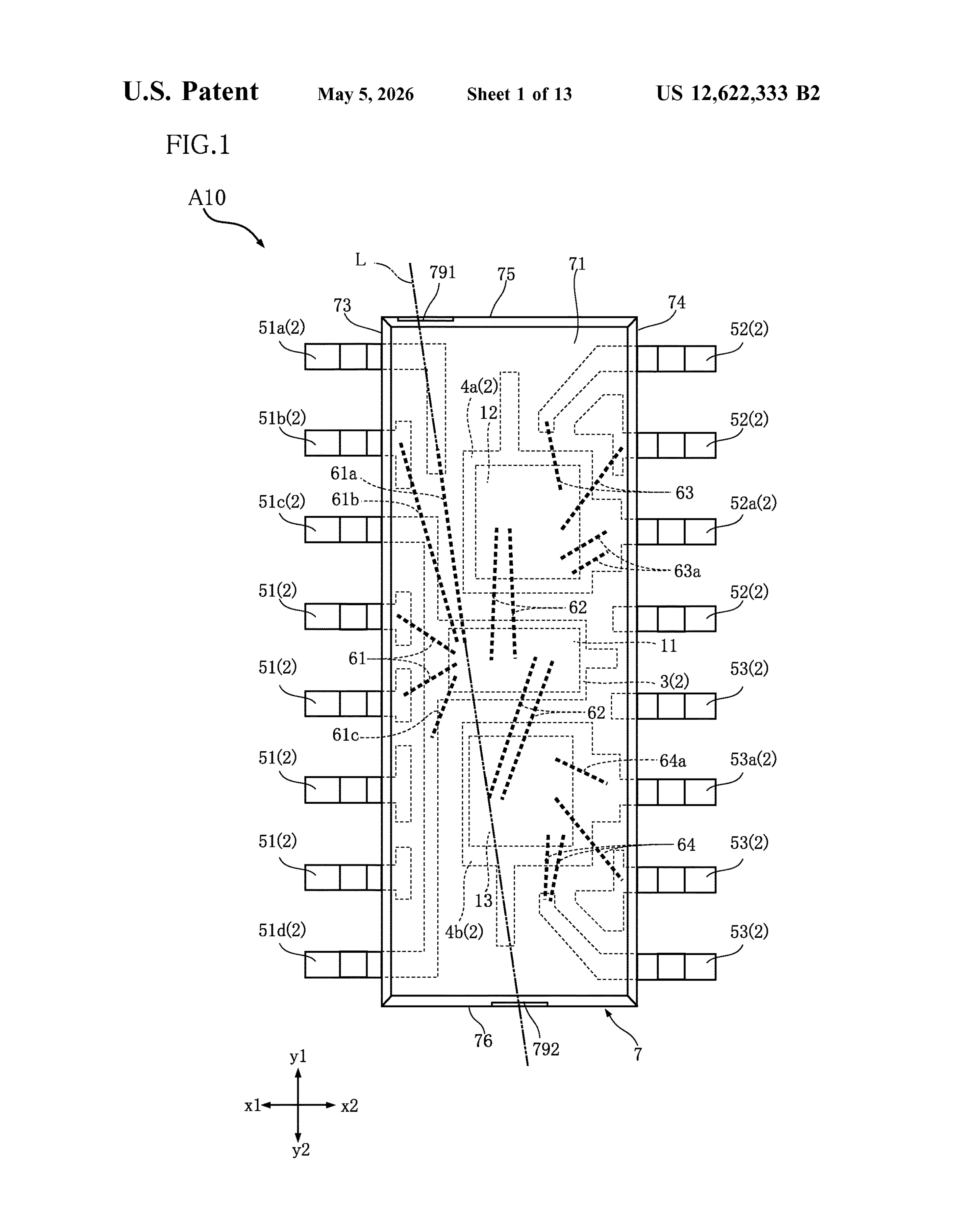
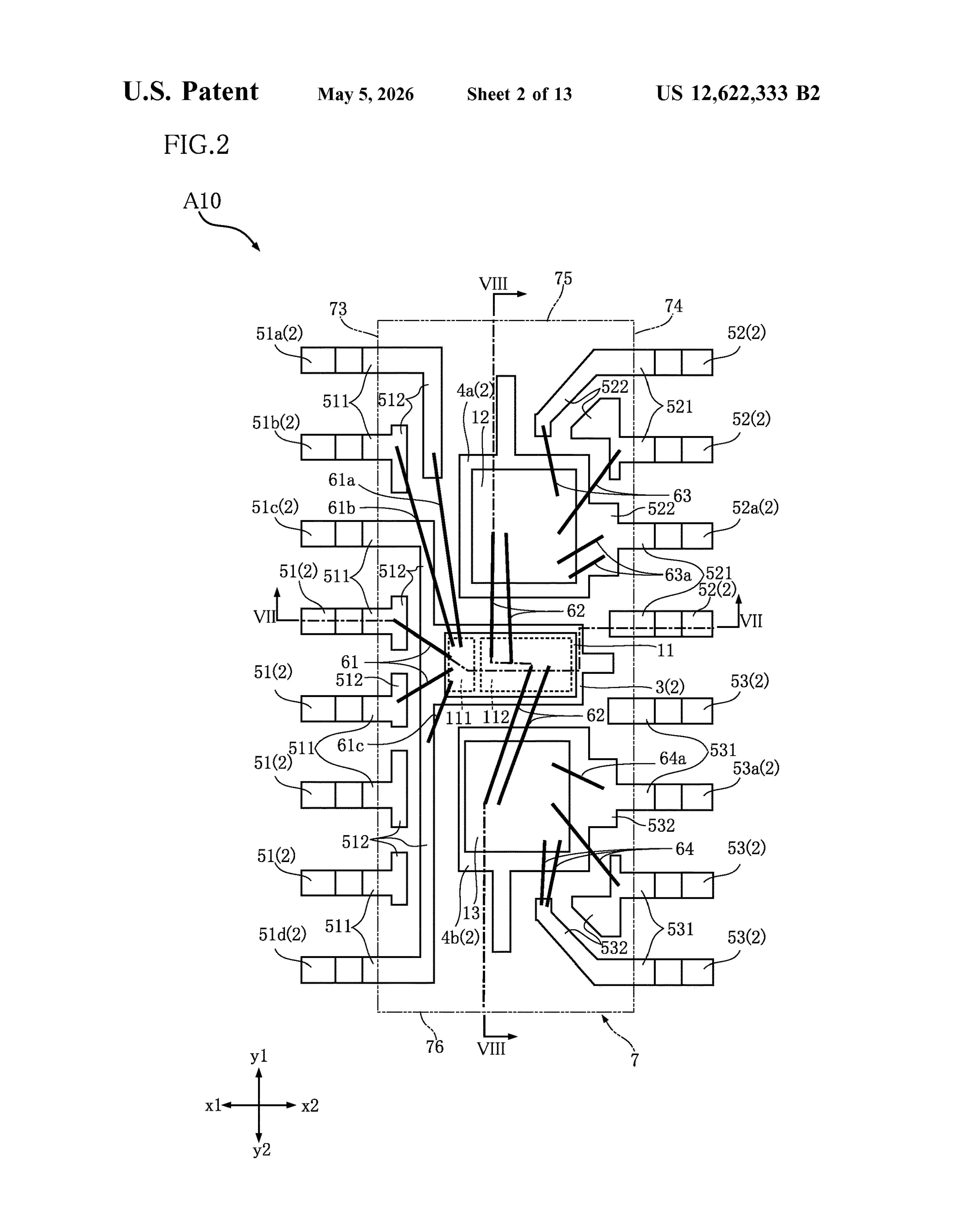
The semiconductor device comprises a conductive support member with a first die pad and a second die pad spaced apart and held at different potentials, a first semiconductor element on the first pad that includes both an input-side circuit and an insulating part for signal transmission with electrical isolation, a second semiconductor element on the second pad that forms the output-side circuit, and sealing resin that covers the assembly while exposing input terminals on one side face and output terminals on the opposite side face.
What carries the argument
The insulating part inside the first semiconductor element, which transmits signals between the input-side circuit and the output-side circuit while maintaining electrical isolation between them.
If this is right
- Input and output circuits can operate at different potentials inside a single molded package without external isolation components.
- Terminals on opposite side faces increase physical separation and simplify board-level creepage distances.
- Signal transfer occurs through the on-element insulator rather than through the conductive support member.
- Multiple circuit functions are integrated while the resin body supplies both mechanical protection and electrical spacing.
Where Pith is reading between the lines
- The layout could reduce board area for isolated drivers or sensors compared with discrete optocoupler solutions.
- Thermal expansion mismatch between the insulating layer and surrounding resin may limit maximum operating temperature or voltage.
- The same separation principle could be applied to packages containing three or more die pads for multi-channel isolation.
Load-bearing premise
The insulating part inside the first semiconductor element can transmit signals reliably while maintaining the required electrical isolation between the input-side and output-side circuits under the voltages and temperatures encountered in normal operation.
What would settle it
Dielectric breakdown or loss of signal integrity between the input and output terminals when the finished device is operated continuously at its rated voltage difference.
Figures
read the original abstract
1 . A semiconductor device comprising: a conductive support member including a first die pad and a second die pad spaced apart from the first die pad in a first sense of a first direction perpendicular to a thickness direction and held at a potential different from a potential of the first die pad; a first semiconductor element mounted on the first die pad; a second semiconductor element mounted on the second die pad and forming an output-side circuit together with the second die pad; a third semiconductor element; and a sealing resin covering at least a portion of the conductive support member, the first semiconductor element and the second semiconductor element, wherein the first semiconductor element includes: a circuit part forming an input-side circuit together with the first die pad; and an insulating part that transmits a signal between the input-side circuit and the output-side circuit and provides electrical insulation between the input-side circuit and the output-side circuit, the conductive support member includes: a plurality of input-side terminals spaced apart from each other in the first direction, at least one of the plurality of input-side terminals being electrically connected to the input-side circuit; and a plurality of output-side terminals spaced apart from each other in the first direction, at least one of the plurality of output-side terminals being electrically connected to the output-side circuit, and the sealing resin includes: a first side face offset in a first sense of a second direction perpendicular to the thickness direction and the first direction, the plurality of input-side terminals protruding from the first side face; a second side face offset in a second sense of the second direction, the plurality of output-side terminals protrudi
Editorial analysis
A structured set of objections, weighed in public.
Referee Report
Summary. The manuscript is a patent claim for a semiconductor device comprising a conductive support member with first and second die pads held at different potentials, a first semiconductor element mounted on the first die pad that contains both an input-side circuit part and an insulating part for signal transmission with electrical isolation, a second semiconductor element mounted on the second die pad forming the output-side circuit, and sealing resin that exposes plural input-side terminals on one lateral face and plural output-side terminals on the opposite lateral face.
Significance. The described package geometry and internal isolation scheme could enable compact, side-by-side placement of input and output circuitry while maintaining galvanic separation, which is useful in power-control or sensor-interface modules. Because the document supplies only a structural description without performance metrics, thermal or voltage ratings, or comparative data, any assessment of practical advantage remains qualitative.
minor comments (2)
- The abstract text is truncated mid-sentence at the description of the second side face; the complete claim language should be supplied for the record.
- Figure references and drawing numbers are absent from the provided text; inclusion of at least one cross-sectional diagram would clarify the relative placement of the insulating part and the terminal protrusions.
Simulated Author's Rebuttal
We thank the referee for the careful reading of the manuscript and for the positive recommendation to accept. The summary accurately captures the structural features of the claimed semiconductor package.
Circularity Check
Patent describes physical structure; no derivations or predictions present
full rationale
The document is a patent claim that asserts only the existence of a particular structural arrangement of die pads, semiconductor elements, insulating parts, terminals, and sealing resin. No equations, fitted parameters, scaling relations, predictions, or self-citations appear anywhere in the text. The claim is therefore self-contained as a direct description of a physical configuration and contains no load-bearing steps that could reduce to their own inputs.
discussion (0)
Sign in with ORCID, Apple, or X to comment. Anyone can read and Pith papers without signing in.