REVIEW 3 major objections 5 minor 15 references
Imaging across the Short-Wave Infra-Red (SWIR) Band via a Flat Multilevel Diffractive Lens
T0 review · 3 major / 5 minor · reviewed 2026-08-14 · deepseek-v4-flash
Pith's one-line read This paper reports a single flat 2.6-micron-thick diffractive lens that focuses and images across the 875-1675 nm SWIR band.
desk verdict A credible SWIR achromatic MDL demonstration whose advertised 800 nm bandwidth is partially extrapolated; refereeable but needs revision to either measure past 1375 nm or narrow the claim. read the letter →
The pith
A machine-rendered reading of the paper's core claim, the machinery that carries it, and where it could break.
The reading
What carries the argument
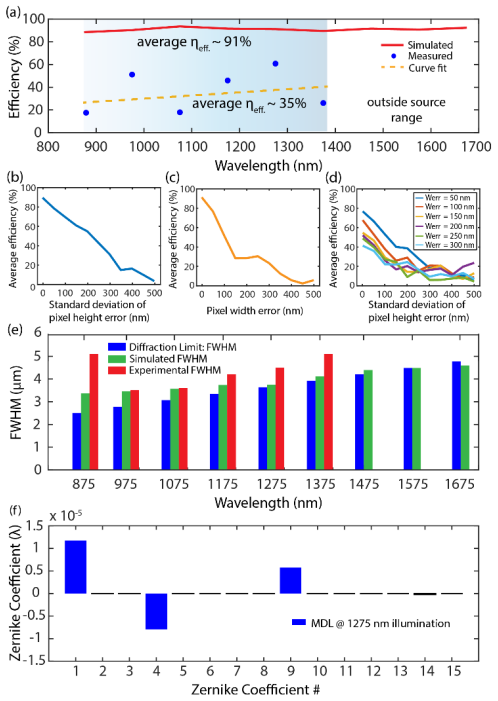
The central object is the multilevel diffractive lens (MDL): a flat diffractive element made of equal-width concentric rings whose heights are quantized into discrete levels, here up to 100 levels with a maximum height of 2.6 µm. The design is driven by a gradient-assisted direct-binary-search algorithm that optimizes the height distribution to maximize wavelength-averaged focusing efficiency across the target band. A fabrication-error simulation accompanies the design, showing that ring-width error is the more serious defect and that combined width and height errors reduce the error tolerance to roughly 100 nm for 50% efficiency. This optimization-error pair is what lets the authors argue the low measured efficiency is a fabrication artifact rather than a fundamental limit.
What would settle it
Shine tunable light at 1450, 1550 and 1650 nm on the same MDL and measure the focal-plane PSF and focusing efficiency. If the focal spot broadens, shifts along the optical axis, or loses efficiency at those wavelengths, the 800 nm achromatic claim is false. Separately, fabricating the same design with ring-width and ring-height errors below roughly 100 nm and remeasuring would test whether 91% efficiency is physically achievable.
Extended reading notes
Core claim
The central claim is that a single flat, polarization-insensitive diffractive surface can replace bulky multi-element refractive lenses for SWIR imaging over an 800 nm bandwidth. The lens consists of concentric rings of equal 3 µm width with heights varying between 0 and 2.6 µm in up to 100 discrete levels; the height profile is chosen by maximizing the wavelength-averaged focusing efficiency, defined as the fraction of incident power falling within three times the FWHM of the focal spot. Experimental point-spread functions at 975, 1175, 1275 and 1375 nm confirm that the lens focuses over the measured range, and the modulation transfer function computed from those PSFs supports imaging use. The authors report that the 800 nm bandwidth is larger than demonstrated infrared metalenses, while the 3 µm minimum feature size is far more forgiving than metalens features near 100 nm, and they show by simulation that fabrication errors of roughly 100 nm in ring height and 400 nm in ring width pull the efficiency from 91% down to the measured 35%.
Load-bearing premise
The whole 875-1675 nm achromatic claim rests on assuming that performance measured only up to about 1375 nm continues unchanged to 1675 nm, since the light source could not reach the long-wavelength end.
Editorial extensions
If this is right
- A single MDL could replace the multi-element refractive objective in a SWIR camera, cutting thickness, weight and cost.
- Because the minimum feature width is 3 µm, the lens can be replicated by polymer imprint lithography rather than requiring the ~100 nm features of metalenses.
- The lens is polarization-insensitive, so it images unpolarized scenes without the efficiency penalty imposed by polarization-selective metalenses.
- If commercial fabrication achieves the error tolerances identified in the simulation, focusing efficiency should rise from the measured ~35% toward the simulated 91%.
- The demonstrated 800 nm band far exceeds the IR bandwidths of the metalens designs used as comparisons, widening the range of wavelengths a single flat lens can serve.
Reading between the lines
- The long-wavelength half of the band, 1375-1675 nm, is unverified; a direct measurement at 1550 nm would test whether focal length and efficiency hold at the band edge.
- The same optimization scheme should scale to other spectral bands, and a natural extension is to fabricate the identical design with a higher-accuracy lithography process to see whether the simulated 91% efficiency is real.
- The comparison to metalenses is favorable partly because the MDL's numerical aperture is modest; whether the 800 nm bandwidth survives at higher NA or larger aperture remains an open question.
- Because the system uses a fixed focal plane, the practical depth of the achromatic window depends on how much axial focal shift occurs across wavelength; the paper's PSF data at only four wavelengths do not fully map that shift.
Signed reviews
Editorial analysis
A structured set of objections, weighed in public.
Referee Report
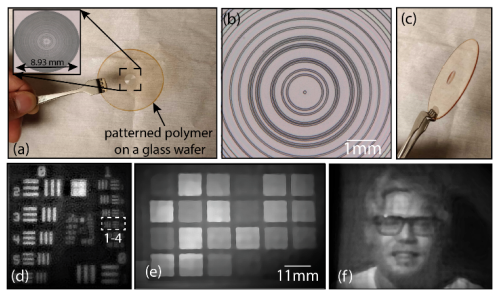
Summary. The paper reports the design, fabrication, and characterization of a flat multi-level diffractive lens (MDL) intended to be achromatic across the short-wave infrared band from 875 nm to 1675 nm. The lens has an 8.93-mm diameter, 25-mm focal length, numerical aperture 0.17, and an active thickness of 2.6 µm. The height profile is obtained by forward optimization of the wavelength-averaged focusing efficiency. The authors present simulated and measured point-spread functions at 975, 1175, 1275, and 1375 nm, a modulation transfer function computed from the measured PSFs, measured and simulated focusing efficiency versus wavelength, imaging of an Air Force resolution chart and other scenes, and a comparison table with prior broadband metalenses. They report a measured average focusing efficiency of about 35% versus a simulated 91%, attribute the discrepancy to fabrication errors in ring height and width, and claim resolved resolution-chart groups up to group 4.
Significance. If the claims are fully supported, the result is significant: a single 2.6-µm-thick diffractive surface with 3-µm minimum features would provide 800-nm-bandwidth, polarization-insensitive imaging in the SWIR with a much larger aperture and focal length than typical metalens demonstrations, and the fabrication simplicity relative to sub-100-nm metalens features is a practical advantage. The paper's strengths include the physical fabrication and measurement of an actual device, quantitative PSF measurements at four wavelengths, a comparison of simulated and measured efficiency, and imaging demonstrations. However, the headline bandwidth claim extends well beyond the measured wavelengths, and the efficiency discrepancy is explained by assumed rather than measured fabrication errors.
major comments (3)
- [Abstract; Sec. 'Fig. 1'; Table 1] The central claim that the lens is achromatic from 875 nm to 1675 nm is not supported by the reported measurements. The measured PSFs, efficiency data, and FWHM data cover only λ = 975, 1175, 1275, and 1375 nm, and the text explicitly states that the supercontinuum source "cuts of for wavelengths above ~1375 nm," so the 1375–1675 nm segment is not experimentally characterized. Despite this, the abstract, the conclusion, and Table 1 present the full 875–1675 nm range as an experimental result. The manuscript must either add measurements in the 1375–1675 nm range or revise the claims to state that the full-band design is simulated while only the 975–1375 nm portion is measured.
- [Fig. 2(a)–(d); text beginning 'To investigate this large discrepancy'] The measured average efficiency of ~35% is far below the simulated ~91%, and the explanation attributed to ring-height errors of ~100 nm and ring-width errors of ~400 nm is not validated by any independent metrology. No measured height profile, width error distribution, or uncertainty analysis is provided, so the error model is a post hoc fit to the efficiency discrepancy rather than a measured characterization. The associated statement that "commercial semiconductor manufacturing can attain errors far smaller than these" is speculative in this context. The authors should provide direct measurements of the fabricated structure or explicitly present the error analysis as a hypothesis with appropriate caveats.
- [Fig. 1(g)–(i); text 'The image sensor was placed in the focal plane'] For a lens claimed to be achromatic, the constancy of focal length across wavelength is a load-bearing property, but the manuscript reports no quantitative focal-length-versus-wavelength data. The PSF images are captured with the sensor placed in a presumably fixed focal plane, yet no measurement of focal shift or refocusing behavior is reported, and the object distance of ~500 mm and sensor distance of ~26 mm are stated only for the imaging demonstration. Without either focal-position measurements or an equivalent analysis, the "achromatic" characterization rests on visual similarity of PSFs rather than on a demonstrated property.
minor comments (5)
- [Fig. 1 caption] The caption lists measured PSFs at λ = 975, 1175, 1275, and 1375 nm, but Figs. 1(g)–(i) contain only three panels; either a panel is missing or the caption incorrectly lists four wavelengths for three images.
- [Fig. 1(j)] The MTF label reads "λ = 875 nm – 1375 nm," but no PSF at 875 nm was measured; the label should reflect the actual measured wavelengths, which are 975–1375 nm.
- [Full text, paragraph on PSF measurement] There is a typo: "cuts of" should be "cuts off."
- [Table 1] The wavelength entry "0.875µm – 1.675µm" uses inconsistent spacing, and the superscript asterisk next to "This work" has no corresponding footnote explaining what the asterisk denotes.
- [Fig. 2(e)] The FWHM measurements are reported without error bars and without comparison to the diffraction-limited FWHM at each wavelength; adding these would strengthen the resolution claim.
Circularity Check
No circularity: the central MDL result is a forward design-and-measurement demonstration; the unmeasured 1375–1675 nm segment and the post-hoc error model are limitations, not circular reductions.
full rationale
The Letter's chain is design optimization followed by fabrication and independent optical characterization, not a derivation in which the claimed output is an input by construction. The height profile was obtained by maximizing wavelength-averaged focusing efficiency with a direct-binary-search algorithm (citing refs 5, 7, 8), and the measured PSF/focusing-efficiency/MTF data at 975, 1175, 1275, and 1375 nm are separate experimental evidence. The simulation used external material dispersion (S1813, ref 5) and the sensor QE as outside inputs, so the design inputs do not already contain the measured efficiencies or the imaging result. The paper explicitly states 'our super-continuum source cuts of for wavelengths above ~1375nm, so we were not able to characterize the PSFs for wavelengths longer than that'; this is an experimental coverage gap for the advertised 1675 nm edge, which should be weighed as a correctness risk, but it is not circular because the claim is not being inferred from the unmeasured wavelengths. The error analysis in Fig. 2(b-d), where '~100nm' height error and '~400nm' width error bring the simulated average efficiency to the measured '~35%', is a post-hoc calibration of an error model to one aggregate efficiency value, not a forward prediction and not load-bearing for the imaging claim. Repeated self-citations (refs 5-11, 17) document prior MDL demonstrations and the optimization method; they are context and method citations, not a self-citation chain used to force the present experimental conclusion. No equation is shown to equal its own input, and no fitted parameter is relabeled as a prediction. Therefore no significant circularity was found.
Assumptions & free parameters
free parameters (1)
- Fabrication error magnitudes =
~100 nm ring-height error, ~400 nm ring-width error
assumptions (3)
- domain assumption The forward diffraction model used in the direct-binary-search optimization accurately computes the focal-plane intensity for the MDL.
- domain assumption The refractive-index dispersion of S1813 photoresist is known and taken from ref. [5].
- domain assumption The performance measured up to 1375 nm is representative of the unmeasured 1375-1675 nm range.
Cite this review
Pith. "Pith review of Imaging across the Short-Wave Infra-Red (SWIR) Band via a Flat Multilevel Diffractive Lens." pith.science (2026). https://pith.science/paper/MLWG76SM
@misc{pith2026190801945,
  author       = {Pith},
  title        = {Pith review of: Imaging across the Short-Wave Infra-Red (SWIR) Band via a Flat Multilevel Diffractive Lens},
  year         = {2026},
  howpublished = {\url{https://pith.science/paper/MLWG76SM}},
  note         = {Machine review of arXiv:1908.01945}
}
read the original abstract
We designed and fabricated a flat multi-level diffractive lens (MDL) that is achromatic in the SWIR band (875nm to 1675nm). The MDL had a focal length of 25mm, aperture diameter of 8.93mm and thickness of only 2.6um. By pairing the MDL with a SWIR image sensor, we also characterized its imaging performance in terms of the point-spread functions, modulation-transfer functions, and still and video imaging.
Figures

Reference graph
Works this paper leans on
-
[1]
Overview of SWIR detectors, cameras and applications
M. P. Hansen, and D. S. Malchow, “Overview of SWIR detectors, cameras and applications”, Proc. SPIE v6939, Thermosense XXX, 693901 (2008)
work page 2008
-
[3]
Optical Systems with Phase Layers
G. G. Slusarev, “Optical Systems with Phase Layers” Soviet Physics-Doclady, Vol. 2, No. 2, pp. 161-163 (1957). Reprinted in: Holographic and Diffractive Lenses and Mirrors, Eds.: T. W. Stone and B. J. Thompson, SPIE Milestone series, Vol. MS 34, pp. 412 – 414 (1991)
work page 1957
-
[4]
Binary optics technology: the theory and design of multilevel diffractive optical elements,
G. J. Swanson, “Binary optics technology: the theory and design of multilevel diffractive optical elements,” Technical Report 854 (MIT Lincoln Laboratory, 1989)
work page 1989
-
[5]
Chromatic-aberration-corrected diffractive lenses for ultra-broadband focusing
P. Wang, N. Mohammad, and R. Menon, “Chromatic-aberration-corrected diffractive lenses for ultra-broadband focusing”, Sci. Rep. 6, 21545 (2016)
work page 2016
-
[6]
Broadband imaging with one planar diffractive lens
N. Mohammad, M. Meem, B. Shen, P. Wang, and R. Menon, “Broadband imaging with one planar diffractive lens”, Sci. Rep. 8 2799 (2018)
work page 2018
-
[7]
Full-color video and still imaging using two flat lenses
M. Meem, A. Majumder, and R. Menon, “Full-color video and still imaging using two flat lenses”, Opt. Exp. 26(21) 26866 (2018)
work page 2018
-
[8]
M. Meem, S. Banerji, A. Majumder, F. G. Vasquez, B. Sensale-Rodriguez, and R. Menon, Broadband lightweight flat lenses for longwave-infrared imaging. arXiv: 1904.09011. (2019)
work page Pith review arXiv 2019
-
[9]
S. Banerji and B. Sensale-Rodriguez, “A Computational Design Framework for Efficient, Fabrication Error-Tolerant, Planar THz Diffractive Optical Elements" Sci. Rep. 9, 5801 (2019)
work page 2019
Show all 15 references
-
[10]
3D-printed diffractive terahertz optical elements through computational design
S. Banerji, and B. Sensale-Rodriguez, “3D-printed diffractive terahertz optical elements through computational design.” In Micro-and Nanotechnology Sensors, Systems, and Applications XI (Vol. 10982, p. 109822X). International Society for Optics and Photonics (2019)
2019
-
[11]
Imaging over an unlimited bandwidth with a single diffractive surface
S. Banerji, M. Meem, A. Majumder, B. Sensale-Rodriguez, and R. Menon, “Imaging over an unlimited bandwidth with a single diffractive surface” arXiv: 1907.06251. (2019)
2019 arXiv
-
[13]
Broadband achromatic dielectric metalenses
S. Shrestha, A. Overvig, M. Lu, A. Stein, N. Yu, “Broadband achromatic dielectric metalenses” Light: Sci. Appl. 2018, 7,
2018
-
[14]
Achromatic metasurface lens at telecommunication wavelengths
M. Khorasaninejad, F. Aieta, P. Kanhaiya, M.A. Kats, P. Genevet, D. Rousso, and F. Capasso, “Achromatic metasurface lens at telecommunication wavelengths.” Nano lett. 15(8), pp.5358-5362 (2015)
2015
-
[15]
Broadband achromatic optical metasurface devices
S. Wang, P.C. Wu, V.C., Su, Y.C., Lai, C.H. Chu, J.W. Chen, S.H. Lu, J. Chen, B. Xu, C.H. Kuan, and T. Li, “Broadband achromatic optical metasurface devices.” Nature communications, 8(1), p.187 (2017)
2017
-
[16]
Plasmonic lattice lenses for multiwavelength achromatic focusing
J. Hu, C.H. Liu, X. Ren, L.J. Lauhon, and T.W. Odom, “Plasmonic lattice lenses for multiwavelength achromatic focusing.” ACS nano, 10(11), pp.10275-10282 (2016)
2016
-
[17]
Imaging with flat optics: metalenses or diffractive lenses?
S. Banerji, M. Meem, A. Majumder, F.G. Vasquez, B. Sensale-Rodriguez and R. Menon, “Imaging with flat optics: metalenses or diffractive lenses?” Optica 6, 805 (2019)
2019
Reviewed August 14, 2026 · model on record in the stance chip above.
Discussion (0). Continue with ORCID to comment.