REVIEW 2 major objections 4 minor 52 references
3D-aCortex: An Ultra-Compact Energy-Efficient Neurocomputing Platform Based on Commercial 3D-NAND Flash Memories
T0 review · 2 major / 4 minor · reviewed 2026-08-14 · deepseek-v4-flash
Pith's one-line read Unmodified commercial 3D-NAND flash can perform neural-network matrix multiplication in the time domain, with 4.34 MB/mm2 storage and ~70 TOps/J energy efficiency.
desk verdict A clever, seriously flawed simulation study: the 3D-NAND time-domain VMM idea is real, but the record-breaking numbers depend on a weight-precision assumption the authors explicitly leave unmodeled. read the letter →
The pith
A machine-rendered reading of the paper's core claim, the machinery that carries it, and where it could break.
The reading
What carries the argument
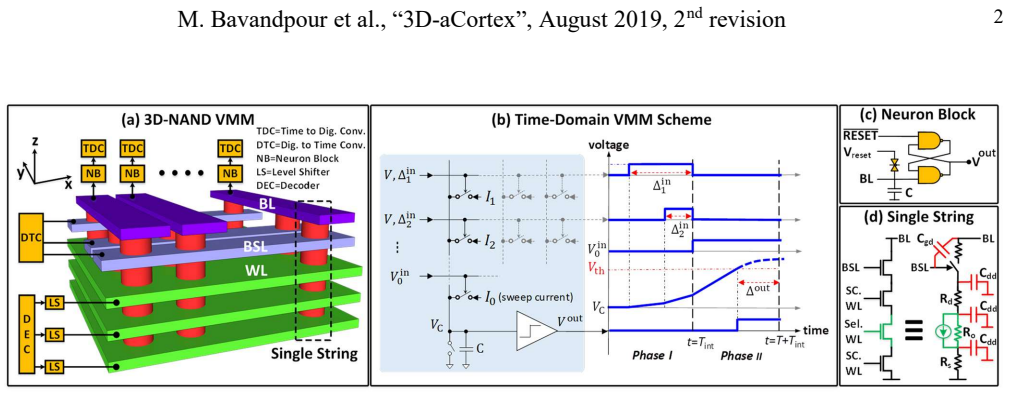
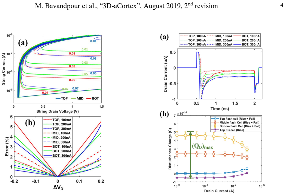
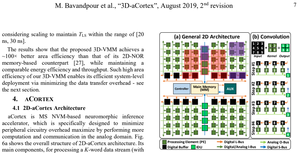
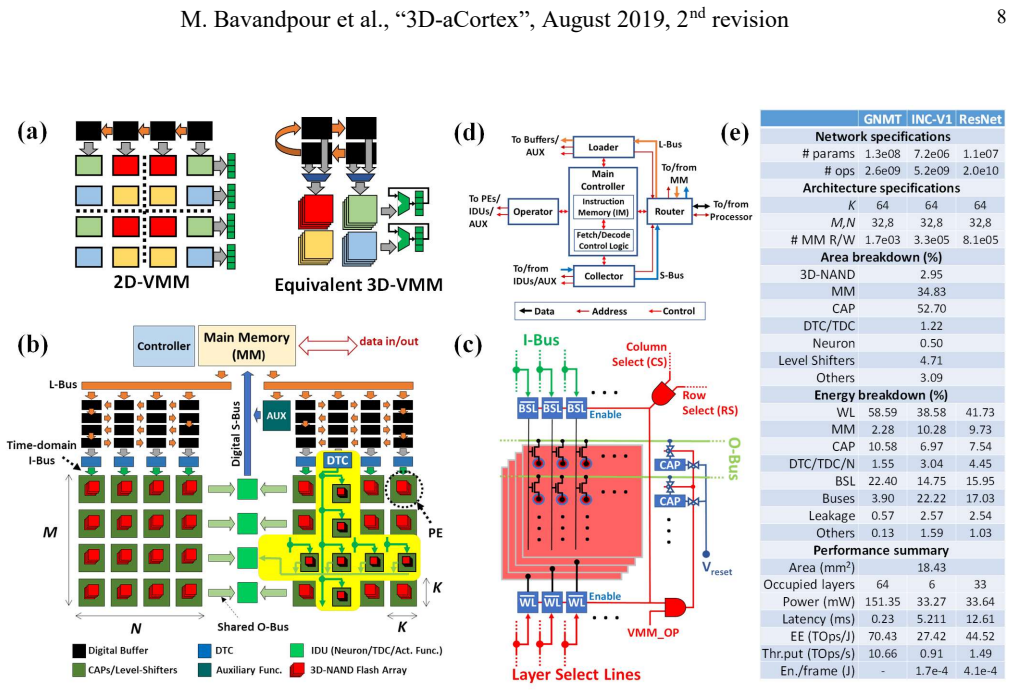
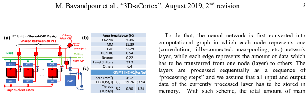
The central object is a time-domain-encoded vector-by-matrix multiplier built from an unmodified 3D-NAND string. Inputs are pulse durations $\Delta_i^{\mathrm{in}}=x_i T$; stored weights $w_{ij}$ are cell currents $I_{ij}$ in $[0,I_{\max}]$. During phase one, pulses on bit-select lines enable row currents, and charge $I_{ij}\Delta_i^{\mathrm{in}}$ accumulates on each bit-line capacitor $C$. During phase two, a constant sweep current $MI_{\max}$ ramps the capacitor voltage until a threshold triggers an SR latch, producing an output pulse width $\Delta_j^{\mathrm{out}}=(1/(MI_{\max}))\sum_i I_{ij}\Delta_i^{\mathrm{in}}$ that encodes the dot product. One memory layer at a time is selected by putting 2 V on its word line and 5 V on the pass word lines, so the compute acts on one x-y plane of the vertical array; the top layer supplies the sweep current. Capacitive coupling from bit-select-line switching is budgeted by reserving extra voltage swing and scaling the output window by a coupling coefficient $\alpha_{\mathrm{cp}}$, while drain-induced barrier lowering is characterized with a small-signal string model. On the system side, 3D-aCortex adapts the earlier 2D aCortex architecture by folding the input shift registers, adding 6-bit output accumulators and barrel shifters, and time-multiplexing VMM operations across memory layers so an entire network can live on-chip.
What would settle it
Program a 64-layer, gate-all-around 3D-NAND block to 16 target current levels per cell, then measure the programmed-current distributions, their retention drift, and read-disturb behavior at the operating voltages used here; if the 16 levels cannot be separated with the assumed tuning accuracy, the 4-bit weight premise and the 3D-aCortex energy and storage numbers fail. A simpler calculation would re-run the paper's error analysis with a realistic per-cell current sigma inserted in place of ideal weights.
Extended reading notes
Core claim
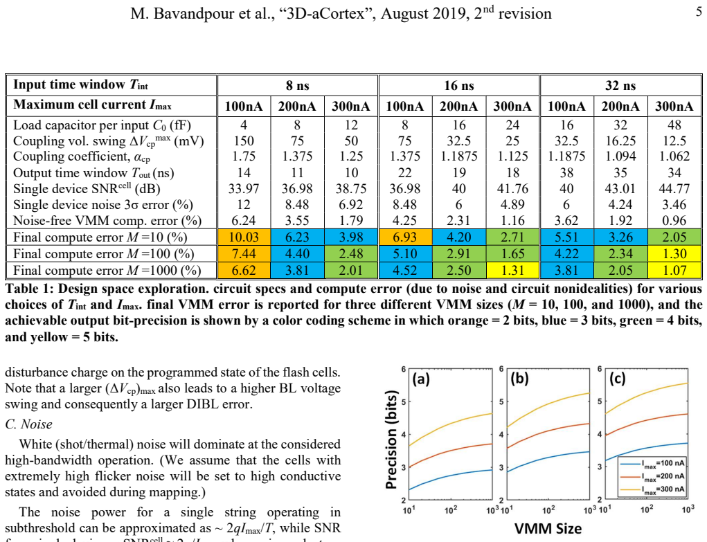
The central claim is that a time-domain VMM design removes the obstacle that kept 3D-NAND out of analog computing: because word lines are shared by entire layers, current-mode readout cannot assign separate inputs to cells in the same layer. Instead, each input $x_i$ becomes a fixed-amplitude pulse of duration $\Delta_i^{\mathrm{in}}=x_i T$ applied to a bit-select line; the cells in a selected x-y layer act as current sources $I_{ij}$ proportional to stored weights; their charges $I_{ij}\Delta_i^{\mathrm{in}}$ are summed on bit-line capacitors; and a second 'sweep' phase turns the summed voltage into an output pulse whose duration is proportional to $y_j=\sum_i w_{ij}x_i$. The paper reports detailed circuit-level SPICE simulations at the 55-nm node including drain-induced barrier lowering, capacitive coupling, noise, process variation, and parasitics, showing compute precision tunable from 2 to 5 bits. It then reports system-level simulations of 3D-aCortex, a processor that maps whole network layers onto the vertical stack of 3D-NAND layers, uses folded input buffers and 6-bit output accumulators to avoid extra memory traffic, and runs Inception-v1, ResNet-152, and GNMT benchmarks at 4-bit compute precision.
Load-bearing premise
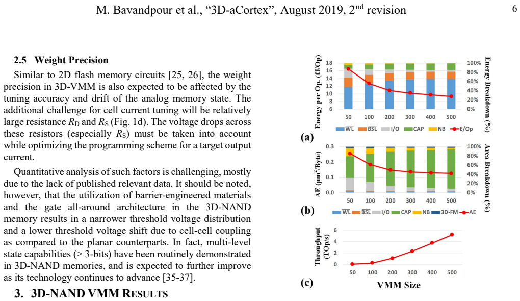
The load-bearing premise is that a commercial 3D-NAND cell can be programmed to hold at least 16 stable, well-separated current levels for analog weights; the paper states that tuning accuracy and drift are not quantitatively modeled, so the system-level precision rests on this unverified capability.
Editorial extensions
If this is right
- Any existing 3D-NAND block could become a neural-network compute engine by adding peripheral circuits only — level shifters, load capacitors, latches, counters — avoiding a redesign of the memory array.
- Because the peripheral circuits are digital, the same design should port to smaller CMOS nodes and to 3D-NAND stacks with more layers, improving energy and density without changing the scheme.
- At 4.34 MB/mm², the stored weights for the largest benchmark networks fit on-chip, removing the off-chip memory traffic that dominates many digital accelerators.
- Sharing one load-capacitor bank across 16 blocks raises storage efficiency to 30.7 MB/mm², at the cost of some energy efficiency and throughput, giving a direct density-versus-performance trade-off.
Reading between the lines
- The paper leaves implicit that, if the 4-bit weight premise is confirmed, the same time-domain scheme should port to other vertical memory arrays with shared word lines, because compute precision is set by cell physics rather than peripheral amplifier gain.
- A direct test the paper does not perform: drive an unmodified commercial 3D-NAND die with an FPGA-based peripheral controller, program known weight patterns, and compare measured output pulse widths with the ideal dot products.
- Because the system-level numbers assume ideal weights, a realistic cell-current spread would lower the effective precision or force a wider output time window; the reported energy and storage figures should therefore be read as an upper bound until tuning error and retention drift are measured.
- Time-multiplexing layer selection makes word-line selection time part of every VMM step, so very tall layer stacks would likely favor larger VMMs per step to amortize that overhead.
Signed reviews
Editorial analysis
A structured set of objections, weighed in public.
Referee Report
Summary. The paper proposes a mixed-signal vector-by-matrix multiplication (VMM) scheme built on unmodified commercial 3D-NAND flash memory arrays, using time-domain encoding of inputs and outputs. The authors analyze circuit-level non-idealities (DIBL, capacitive coupling, noise) with a behavioral compact model and SPICE simulations, and then present a system-level neuromorphic inference processor, 3D-aCortex, that uses these VMM blocks. Reported results include an area efficiency of 0.14 um^2/byte, ~10 fJ/Op VMM energy, and system-level metrics of 4.34 MB/mm^2 storage efficiency, 70.43 TOps/J energy efficiency, and 10.66 TOps/s throughput for representative DNN/RNN benchmarks at 4-bit precision.
Significance. If the reported results hold, this work would represent a major advance in analog in-memory computing: it would show that a commercially mature memory technology can serve as the compute substrate for high-density, energy-efficient neuromorphic inference without array modification. The paper's strengths are its detailed treatment of compute precision (DIBL, capacitive coupling, noise, process variation), its use of a compact model calibrated to published experimental I-V data, its transparent reporting of design points and operating assumptions, and its system-level architecture design with a concrete mapping algorithm. However, the central claim depends on an unverified physical premise: that 3D-NAND cells can be programmed to at least 4-bit analog weight precision with acceptable tuning accuracy and drift. The paper explicitly states that quantitative analysis of this factor is challenging due to lack of published data, and all headline performance numbers are computed assuming ideal 4-bit weights.
major comments (2)
- [§2.5, §3, §5, Table 2] The load-bearing assumption of 4-bit analog weight precision is explicitly not quantified. Section 2.5 states that 'Quantitative analysis of such factors is challenging, mostly due to the lack of published relevant data,' and then appeals to storage-level MLC capability (>3 bits) in commercial 3D-NAND. However, storage-level threshold-voltage distributions with ECC do not demonstrate that a cell in a 64-cell series string can be tuned to 16 stable analog current levels under the specific bias schedule (2 V selected WL, 5 V pass WL, fixed BL swing) used in §2.2, especially with series resistances RD and RS. Table 1 and Fig. 4 include DIBL, coupling, and noise, but not weight-programming error or drift. Because the system-level claims in Table 2 (e.g., 4.34 MB/mm^2, 70.43 TOps/J) are all computed at 4-bit weights, the record-breaking comparison inherits this unverified assumption. The authors should either provide experimental evidence of analog tuning accuracy and drift (even on a small test array) or clearly present the system-level numbers as projections conditional on this assumption, with a sensitivity analysis to reduced weight precision.
- [§2.3C, Table 1] The noise analysis assumes that cells with extremely high flicker noise will be identified and mapped to high-conductive states, so that flicker noise can be neglected. This is an untested mapping assumption: a real array would have a distribution of flicker noise, and remapping could be constrained by the limited number of high-conductive cells and by the need to maintain the target weight distribution. If this assumption fails, the compute errors in Table 1 and the resulting precision/energy trade-offs would be optimistic. A sensitivity analysis or a discussion of the mapping overhead would be needed to support the reported precision results.
minor comments (4)
- [Abstract, §3] The abstract highlights a 5-bit VMM example, while the system-level results and Table 2 are all presented for 4-bit precision. Please clarify the relationship between these precision choices and why the 4-bit setting is used for the final comparisons.
- [§6, paragraph 1] The text reports 'energy efficiency of our 3D-VMM is very high - for example, ~9 fF/Op' – 'fF' appears to be a typo for 'fJ' (femtocoulomb is not an energy unit). Please correct.
- [§2.1, Eq. (3)] In Eq. (3), the output pulse duration is written as Δjout (Delta_j^out) but the subscript j is missing in the displayed equation; the notation should be defined consistently with the text.
- [§4.1, first paragraph] The phrase 'peripheral circuitry overhead maximize by performing' is grammatically incomplete; it should read 'maximized by performing'.
Circularity Check
No circular derivation: time-domain VMM and compact model are independently grounded; the 4-bit weight premise is an explicitly unverified assumption, not a circular input.
full rationale
The derivation chain is self-contained against external benchmarks. The time-domain VMM principle is cited to prior work [27] by the same group, but it is a published design technique applied here to a new 3D-NAND substrate; it is not a result whose prediction is equivalent to the paper's inputs. The 3D-NAND compact model [38] is also from the same group, but Section 2.3 states it 'accurately reproduces the experimental string current characteristics [43,44]', where [43,44] are external measurements, so the model is independently calibrated rather than a self-citation chain. Compute precision is obtained by SPICE simulation over randomized inputs/weights and physical parasitics, with parameters (Imax, Tint) selected from a design-space table, not fitted to the headline efficiency metrics; area/energy/throughput estimates follow from post-layout circuit specifications and Cacti-based memory models. The most important caveat is in Section 2.5: 'Quantitative analysis of such factors is challenging, mostly due to the lack of published relevant data' regarding weight tuning accuracy and drift, and Table 1/Fig. 4 report precision without weight-programming error or drift. That is an unsupported physical assumption on which the 4-bit system numbers depend, but it is not circular: the paper explicitly conditions the analysis on demonstrated multi-level-cell capability rather than deriving that capability from its own output. The headline 'record-breaking' claims are conditional on an unverified premise, which is a correctness risk, not a circularity defect.
Assumptions & free parameters
free parameters (5)
- Imax (maximum cell current) =
300 nA
- Tint (input time window) =
16 ns
- BL voltage operating points (Vth, ΔVcmp) =
0.6 V, 0.2 V
- (QD)max (worst-case coupling disturbance charge) =
6e-16 C
- Architecture dimensions (K, M, N) =
K=64, M=32, N=8
assumptions (5)
- domain assumption The behavioral compact model [38] accurately represents the commercial 64-layer macaroni-type 3D-NAND memory.
- ad hoc to paper The 3D-NAND cells can be programmed to at least 4-bit analog weight precision with acceptable drift.
- domain assumption The top layer of cells can be programmed to a uniform current Imax for the sweep phase.
- ad hoc to paper Cells with high flicker noise can be avoided by mapping them to high-conductive states.
- domain assumption CACTI estimates for eDRAM and SRAM accurately capture main memory and instruction memory costs.
Cite this review
Pith. "Pith review of 3D-aCortex: An Ultra-Compact Energy-Efficient Neurocomputing Platform Based on Commercial 3D-NAND Flash Memories." pith.science (2026). https://pith.science/paper/JTUV3J32
@misc{pith2026190802472,
  author       = {Pith},
  title        = {Pith review of: 3D-aCortex: An Ultra-Compact Energy-Efficient Neurocomputing Platform Based on Commercial 3D-NAND Flash Memories},
  year         = {2026},
  howpublished = {\url{https://pith.science/paper/JTUV3J32}},
  note         = {Machine review of arXiv:1908.02472}
}
read the original abstract
The first contribution of this paper is the development of extremely dense, energy-efficient mixed-signal vector-by-matrix-multiplication (VMM) circuits based on the existing 3D-NAND flash memory blocks, without any need for their modification. Such compatibility is achieved using time-domain-encoded VMM design. Our detailed simulations have shown that, for example, the 5-bit VMM of 200-element vectors, using the commercially available 64-layer gate-all-around macaroni-type 3D-NAND memory blocks designed in the 55-nm technology node, may provide an unprecedented area efficiency of 0.14 um2/byte and energy efficiency of ~10 fJ/Op, including the input/output and other peripheral circuitry overheads. Our second major contribution is the development of 3D-aCortex, a multi-purpose neuromorphic inference processor that utilizes the proposed 3D-VMM blocks as its core processing units. We have performed rigorous performance simulations of such a processor on both circuit and system levels, taking into account non-idealities such as drain-induced barrier lowering, capacitive coupling, charge injection, parasitics, process variations, and noise. Our modeling of the 3D-aCortex performing several state-of-the-art neuromorphic-network benchmarks has shown that it may provide the record-breaking storage efficiency of 4.34 MB/mm2, the peak energy efficiency of 70.43 TOps/J, and the computational throughput up to 10.66 TOps/s. The storage efficiency can be further improved seven-fold by aggressively sharing VMM peripheral circuits at the cost of slight decrease in energy efficiency and throughput.
Figures
Figures from the paper (4 more)
Reference graph
Works this paper leans on
-
[27]
Energy- Efficient Time-Domain Vector-by-Matrix Multiplier for Neurocomputing and Beyond,
M. Bavandpour, M.R. Mahmoodi, and D.B. Strukov, “Energy- Efficient Time-Domain Vector-by-Matrix Multiplier for Neurocomputing and Beyond,” in: IEEE Transactions on Circuits and Systems II: Express Briefs, 2019. doi: 10.1109/TCSII.2019.2891688
arXiv 2019
-
[1]
Deep Learning for IoT Big Data and Streaming Analytics: A Survey,
M. Mohammadi, A. Al-Fuqaha, S. Sorour, and M. Guizani, "Deep Learning for IoT Big Data and Streaming Analytics: A Survey,” in IEEE Communications Surveys & Tutorials, vol. 20, no. 4, pp. 2923-2960, 2018
work page 2018
-
[2]
Y. LeCun, Y. Bengio, and G. Hinton, "Deep learning,” Nature, vol. 521, pp. 436-444, May 2015
work page 2015
-
[3]
ImageNet classification with deep convolutional neural networks,
A. Krizhevsky, I. Sutskever, and G. Hinton, "ImageNet classification with deep convolutional neural networks,” Adv. in Neural Info. Proc. Sys., pp. 1097-1105, 2012
work page 2012
-
[4]
Going deeper with convolutions,
C. Szegedy, W. Liu, Y. Jia, P. Sermanet, S. Reed, D. Anguelov, D. Erhan, V. Vanhoucke, and A. Rabinovich, "Going deeper with convolutions,” 2015 IEEE Conference on Computer Vision and Pattern Recognition (CVPR), Boston, MA, pp. 1-9, 2015
work page 2015
-
[5]
Deep residual learning for image recognition,
K. He, X. Zhang, S. Ren, and J. Sun, "Deep residual learning for image recognition,” IEEE Conf. on Comp. Vision and Pat. Rec., pp. 770-778, 2016
work page 2016
-
[6]
Google's neural machine translation system: Bridging the gap between human and machine translation,
Y. Wu, M. Schuster, Z. Chen, Q.V. Le, M. Norouzi, W. Macherey, M. Krikun, Y. Cao, Q. Gao, K. Macherey, and J. Klingner, "Google's neural machine translation system: Bridging the gap between human and machine translation,” arXiv preprint arXiv:1609.08144, 2016
arXiv 2016
-
[7]
In-datacenter performance analysis of a tensor processing unit,
N.P. Jouppi, C. Young, N. Patil, D. Patterson, G. Agrawal, R. Bajwa, S. Bates, S. Bhatia, N. Boden, A. Borchers, and R. Boyle, “In-datacenter performance analysis of a tensor processing unit,” in ACM/IEEE 44th Annual International Symposium on Computer Architecture (ISCA), Toronto, ON, pp. 1-12, 2017
work page 2017
Show all 52 references
-
[8]
DaDianNao: A Machine-Learning Supercomputer,
Y. Chen, T. Luo, S. Liu, S. Zhang, L. He, J. Wang, L. Li, T. Chen, Z. Xu, N. Sun, and O. Temam, “DaDianNao: A Machine-Learning Supercomputer,” in 47th Annual IEEE/ACM International Symposium on Microarchitecture, Cambridge, pp. 609-622, 2014
2014
-
[9]
Eyeriss: An Energy-Efficient Reconfigurable Accelerator for Deep Convolutional Neural Networks,
Y.H. Chen, T. Krishna, J.S. Emer, and V. Sze, “Eyeriss: An Energy-Efficient Reconfigurable Accelerator for Deep Convolutional Neural Networks,” in IEEE Journal of Solid- State Circuits, vol. 52, no. 1, pp. 127-138, 2017
2017
-
[10]
ARM ML processor (https://www.arm.com/ products/ processors/machine-learning); Intel Mobileye (https://www.mobileye.com/en-us/); Google Edge TPU (https://cloud.google.com/edge-tpu/)
-
[11]
14.5 envision: A 0.26-to-10tops/w subword-parallel dynamic-voltage-accuracy- frequency-scalable convolutional neural network processor in 28nm fdsoi,
B. Moons, U. Roel, D. Wim, and V. Marian, “14.5 envision: A 0.26-to-10tops/w subword-parallel dynamic-voltage-accuracy- frequency-scalable convolutional neural network processor in 28nm fdsoi,” In 2017 IEEE International Solid-State Circuits Conference (ISSCC), pp. 246-247, 2017
2017
-
[12]
Loihi: a neuromorphic manycore processor with on-chip learning,
M. Davies, N. Srinivasa,T. H. Lin, G. Chinya, Y. Cao, S. H. Choday, G. Dimou, P. Joshi, N. Imam, S. Jain, and Y. Liao, “Loihi: a neuromorphic manycore processor with on-chip learning,” IEEE Micro, 38(1), pp.82-99, 2018
2018
-
[13]
A million spiking-neuron integrated circuit with a scalable communication network and interface,
P. A. Merolla, J. V. Arthur, R. Alvarez-Icaza, A. S. Cassidy, J. Sawada, F. Akopyan, B. L. Jackson, N. Imam, C. Guo, Y. Nakamura, and B. Brezzo, “A million spiking-neuron integrated circuit with a scalable communication network and interface,” Science, 345(6197), pp.668-673, 2014
2014
-
[14]
UNPU: An Energy-Efficient Deep Neural Network Accelerator with Fully Variable Weight bit Precision,
J. Lee, C. Kim, S. Kang, D. Shin, S. Kim, and H.J. Yoo, “UNPU: An Energy-Efficient Deep Neural Network Accelerator with Fully Variable Weight bit Precision,” IEEE Journal of Solid-State Circuits, vol. 54, no.1, pp.173-185, 2018
2018
-
[15]
Quantized neural networks: Training neural networks with low precision weights and activations,
I. Hubara, M. Courbariaux, D. Soudry, R. El-Yaniv, and Y. Bengio, “Quantized neural networks: Training neural networks with low precision weights and activations,” arXiv preprint arXiv:1609.07061, Sep. 2016
2016 arXiv
-
[16]
Discovering Low-Precision Networks Close to Full-Precision Networks for Efficient Embedded Inference,
J.L. McKinstry, S.K. Esser, R. Appuswamy, D. Bablani, J.V. Arthur, I.B. Yildiz, and D.S. Modha, “Discovering Low-Precision Networks Close to Full-Precision Networks for Efficient Embedded Inference,” arXiv preprint arXiv:1809.04191, 2018
2018 arXiv
-
[17]
Alternating Multi-bit Quantization for Recurrent Neural Networks,
C. Xu, J. Yao, Z. Lin, W. Ou, Y. Cao, Z. Wang, and H. Zha, “Alternating Multi-bit Quantization for Recurrent Neural Networks,” arXiv preprint arXiv:1802.00150, 2018
2018 arXiv
-
[18]
Mixed-signal neuromorphic inference accelerators: Recent results and future prospects,
M. Bavandpour, M.R. Mahmoodi, H. Nili, F.M. Bayat, M. Prezioso, A. Vincent, D.B. Strukov, and K.K. Likharev, “Mixed-signal neuromorphic inference accelerators: Recent results and future prospects,” in: Proc. IEDM'18, San Francisco, CA, Dec. 2018
2018
-
[19]
Dot-product engine for neuromorphic computing: programming 1T1M crossbar to accelerate matrix-vector multiplication,
M. Hu, J.P. Strachan, Z. Li, E.M. Grafals, N. Davila, C. Graves, S. Lam, N. Ge, J.J. Yang, and R.S. Williams, “Dot-product engine for neuromorphic computing: programming 1T1M crossbar to accelerate matrix-vector multiplication,” in: Proc. DAC'16, Austin, TX, pp.1-6, 2016
2016
-
[20]
Implementation of multilayer perceptron network with highly uniform passive memristive crossbar circuits
F. Merrikh Bayat, M. Prezioso, B. Chakrabarti, H. Nili, I. Kataeva, and D. Strukov, "Implementation of multilayer perceptron network with highly uniform passive memristive crossbar circuits", Nature Communications 9, art. 2331, 2018
2018
-
[21]
Face classification using electronic synapses,
P. Yao, H. Wu, B. Gao, S. B. Eryilmaz, X. Huang, W. Zhang, Q. Zhang, N. Deng, L. Shi, H. S. P. Wong, and H. Qian, H., “Face classification using electronic synapses,” Nature communications, 8, p.15199, 2017
2017
-
[22]
A functional hybrid memristor crossbar-array/CMOS system for data storage and neuromorphic applications,
K. H. Kim, S. Gaba, D. Wheeler, J. M. Cruz-Albrecht, T. Hussain, N. Srinivasa, and W. Lu, “A functional hybrid memristor crossbar-array/CMOS system for data storage and neuromorphic applications,” Nano letters, 12(1), pp.389-395, 2011. M. Bavandpour et al., “3D-aCortex”, Augus...
2011
-
[23]
Experimental Demonstration and Tolerancing of a Large-Scale Neural Network (165,000 Synapses), using Phase-Change Memory as the Synaptic Weight Element,
G.W. Burr, R.M. Shelby, S. Sidler, C. Di Nolfo, J. Jang, I. Boybat, R.S. Shenoy, P. Narayanan, K. Virwani, E.U. Giacometti, and B.N. Kurdi, “Experimental Demonstration and Tolerancing of a Large-Scale Neural Network (165,000 Synapses), using Phase-Change Memory as the Synaptic...
2014
-
[24]
Neuromorphic computing with multi- memristive synapses
I. Boybat, M. L. Gallo, S. R. Nandakumar, T. Moraitis, T. Parnell, T. Tuma, B. Rajendran, Y. Leblebici, A. Sebastian, and E. Eleftheriou, “Neuromorphic computing with multi- memristive synapses”, Nature Communications, vol. 9 (1), art. 2514, 2018
2018
-
[25]
Fast, energy-efficient, robust, and reproducible mixed-signal neuromorphic classifier based on embedded NOR flash memory technology,
X. Guo, F.M. Bayat, M. Bavandpour, M. Klachko, M.R. Mahmoodi, M. Prezioso, K.K. Likharev, and D.B. Strukov, “Fast, energy-efficient, robust, and reproducible mixed-signal neuromorphic classifier based on embedded NOR flash memory technology,” in: Proc. IEDM'17, San Francisco, ...
2017
-
[26]
An ultra low energy internally analog, externally digital vector-matrix multiplier circuit based on NOR flash memory technology,
M.R. Mahmoodi, and D.B. Strukov, “An ultra low energy internally analog, externally digital vector-matrix multiplier circuit based on NOR flash memory technology,” in: Proceedings of the 55th Annual Design Automation Conference, p. 22. ACM, 2018
2018
-
[28]
Finding a roadmap to achieve large neuromorphic hardware systems,
J. Hasler, and H. Marr, “Finding a roadmap to achieve large neuromorphic hardware systems,”, Front. Neurosci., vol. 7, art. 118, 2013
2013
-
[29]
A highly dense, low power, programmable analog vector-matrix multiplier: The FPAA implementation
C. R. Schlottmann, and P. E. Hasler, “A highly dense, low power, programmable analog vector-matrix multiplier: The FPAA implementation”, IEEE JETCAS, vol. 1, pp. 403-411, 2011
2011
-
[30]
Sub-microwatt analog VLSI trainable pattern classifier
S. Chakrabartty, and G. Cauwenberghs, “Sub-microwatt analog VLSI trainable pattern classifier”, IEEE JSSC, vol. 42, pp. 1169-1179, 2007
2007
-
[31]
System and Methods for Mixed-Signal Computing,
L. Fick, E.C. Manar, S. Skrzyniarz, and D. Fick, Mythic Inc. “System and Methods for Mixed-Signal Computing,” U.S. Patent Application 10/255,205, 2019
2019
-
[32]
Systems and Methods for Customizing Neural Networks,
K F. Busch, P. Vorenkamp, and S.W. Bailey, Syntiant Corp. “Systems and Methods for Customizing Neural Networks,” U.S. Patent Application 16/164,671, 2019
2019
-
[33]
Superflash Technology Overview
“Superflash Technology Overview”, SST, Inc., available online at https://www.sst.com/technology/sst-superflash- technology
-
[34]
Reviewing the evolution of the NAND flash technology,
C.M. Compagnoni, A. Goda, A.S. Spinelli, P. Feeley, A.L. Lacaita, and A. Visconti, “Reviewing the evolution of the NAND flash technology,” Proc. IEEE, vol. 105, no. 9, pp. 1609-–1633, 2017
2017
-
[35]
Three-Dimensional 128 Gb MLC Vertical nand Flash Memory With 24-WL Stacked Layers and 50 MB/s High- Speed Programming,
K.T. Park, S. Nam, D. Kim, P. Kwak, D. Lee, Y.H. Choi, M.H. Choi, D.H. Kwak, D.H. Kim, M.S. Kim, and H.W. Park, “Three-Dimensional 128 Gb MLC Vertical nand Flash Memory With 24-WL Stacked Layers and 50 MB/s High- Speed Programming,” in IEEE Journal of Solid-State Circuits, vol...
2015
-
[36]
A 512Gb 3b/cell 64-stacked WL 3D V-NAND flash memory,
C. Kim, D.H. Kim, W. Jeong, H.J. Kim, I.H. Park, H.W. Park, J. Lee, J. Park, Y.L. Ahn, J.Y. Lee, and S.B. Kim, “A 512Gb 3b/cell 64-stacked WL 3D V-NAND flash memory,” in IEEE International Solid-State Circuits Conference (ISSCC), San Francisco, CA, pp. 202-203, 2017
2017
-
[37]
A 1.33Tb 4-bit/Cell 3D-Flash Memory on a 96-Word-Line-Layer Technology,
N. Shibata, K. Kanda, T. Shimizu, J. Nakai, O. Nagao, N. Kobayashi, M. Miakashi, Y. Nagadomi, T. Nakano, T. Kawabe, and T. Shibuya, “A 1.33Tb 4-bit/Cell 3D-Flash Memory on a 96-Word-Line-Layer Technology,” in IEEE International Solid-State Circuits Conference (ISSCC), San Fran...
2019
-
[38]
A Behavioral Compact Model for Static Characteristics of 3D NAND Flash Memory,
S. Sahay, and D. B. Strukov, “A Behavioral Compact Model for Static Characteristics of 3D NAND Flash Memory," in: IEEE Electron Device Letters , 2019. doi: 10.1109/LED.2019.2901211
2019
-
[39]
Three-Dimensional nand Flash for Vector-Matrix Multiplication,
P. Wang, F. Xu, B. Wang, B. Gao, H. Wu, H. Qian, and S. Yu, “Three-Dimensional nand Flash for Vector-Matrix Multiplication,” in IEEE Transactions on Very Large Scale Integration (VLSI) Systems , 2018. doi: 10.1109/TVLSI.2018.2882194
2018
-
[40]
Time- mode circuits for analog computation,
V. Ravinuthula, V. Garg, J.G. Harris, and J.A. Fortes, “Time- mode circuits for analog computation,” Int. J. Circ. Theor. App., vol. 37, pp. 631-659, Jun. 2009
2009
-
[41]
A Time-domain Analog Weighted-sum Calculation Model for Extremely Low Power VLSI Implementation of Multi-layer Neural Networks,
Q. Wang, H. Tamukoh, and T. Morie, “A Time-domain Analog Weighted-sum Calculation Model for Extremely Low Power VLSI Implementation of Multi-layer Neural Networks,” in: arXiv preprint arXiv:1810.06819, 2018
2018 arXiv
-
[42]
Silicon nanodisk array with a fin field-effect transistor for time-domain weighted sum calculation toward massively parallel spiking neural networks,
T. Tohara, H. Liang, H. Tanaka, M. Igarashi, S. Samukawa, K. Endo, Y. Takahashi, and T. Morie, “Silicon nanodisk array with a fin field-effect transistor for time-domain weighted sum calculation toward massively parallel spiking neural networks,” APEX, vol. 9, art. 034201, 2016
2016
-
[43]
Characterization and Modeling of Temperature Effects in 3-D NAND Flash Arrays—Part I: Polysilicon-Induced Variability,
D. Resnati, A. Mannara, G. Nicosia, G.M. Paolucci, P. Tessariol, A.S. Spinelli, A.L. Lacaita, and C.M. Compagnoni, “Characterization and Modeling of Temperature Effects in 3-D NAND Flash Arrays—Part I: Polysilicon-Induced Variability,” IEEE Transactions on Electron Devices, vo...
2018
-
[44]
Investigation and Compact Modeling of the Time Dynamics of the GIDL-Assisted Increase of the String Potential in 3-D NAND Flash Arrays,
G. Malavena, A.L. Lacaita, A.S. Spinelli, and C.M. Compagnoni, “Investigation and Compact Modeling of the Time Dynamics of the GIDL-Assisted Increase of the String Potential in 3-D NAND Flash Arrays,” IEEE Transactions on Electron Devices, vol. 65, no. 7, pp. 2804-2811, July 2018
2018
-
[45]
CACTI 6.0: A Tool to Understand Large Caches,
N. Muralimanohar, R. Balasubramonian, and N.P. Jouppi, “CACTI 6.0: A Tool to Understand Large Caches," Technical Report. HP Labs, HPL-2009-85, 2009
2009
-
[46]
ISAAC: A Convolutional Neural Network Accelerator with In-Situ Analog Arithmetic in Crossbars,
A. Shafiee, A. Nag, N. Muralimanohar, R. Balasubramonian, J.P. Strachan, M. Hu, R.S. Williams, and V. Srikumar, “ISAAC: A Convolutional Neural Network Accelerator with In-Situ Analog Arithmetic in Crossbars,” in ACM/IEEE 43rd Annual International Symposium on Computer Architec...
2016
-
[47]
PUMA: A programmable ultra-efficient memristor- based accelerator for machine learning inference,
A. Ankit, I.E. Hajj, S.R. Chalamalasetti, G. Ndu, M. Foltin, R.S. Williams, P. Faraboschi, J.P. Strachan, K. Roy, and D.S. Milojicic, “PUMA: A programmable ultra-efficient memristor- based accelerator for machine learning inference,” in arXiv preprint arXiv:1901.10351 (2019)
2019 arXiv
-
[48]
Harmonica: A Framework of Heterogeneous Computing Systems With Memristor-Based Neuromorphic Computing Accelerators,
X. Liu, M. Mao, B. Liu, B. Li, Y. Wang, H. Jiang, M. Barnell, Q. Wu, J. Yang, H. Li, and Y. Chen, “Harmonica: A Framework of Heterogeneous Computing Systems With Memristor-Based Neuromorphic Computing Accelerators,” in IEEE Transactions on Circuits and Systems I: Regular Paper...
2016
-
[49]
PipeLayer: A Pipelined ReRAM-Based Accelerator for Deep Learning,
L. Song, X. Qian, H. Li, and Y. Chen, “PipeLayer: A Pipelined ReRAM-Based Accelerator for Deep Learning,” in IEEE International Symposium on High Performance Computer Architecture (HPCA), Austin, TX, pp. 541-552, 2017
2017
-
[50]
PRIME: A Novel Processing-in-Memory Architecture for Neural Network Computation in ReRAM-Based Main Memory,
P. Chi, S. Li, C. Xu, T. Zhang, J. Zhao, Y. Liu, Y. Wang, and Y. Xie, “PRIME: A Novel Processing-in-Memory Architecture for Neural Network Computation in ReRAM-Based Main Memory,” in ACM/IEEE 43rd Annual International Symposium on Computer Architecture (ISCA), Seoul, pp. 27- 39, 2016
2016
-
[51]
RAPIDNN: In-Memory Deep Neural Network Acceleration Framework,
M. Imani, M. Samragh, Y. Kim, S. Gupta, F. Koushanfar, and T. Rosing, “RAPIDNN: In-Memory Deep Neural Network Acceleration Framework,” in arXiv preprint arXiv:1806.05794 (2018)
2018 arXiv
-
[52]
PROMISE: An End-to- End Design of a Programmable Mixed-Signal Accelerator for Machine-Learning Algorithms,
P. Srivastava, M. Kang, S.K. Gonugondla, S. Lim, J. Choi, V. Adve, N.S. Kim, and N. Shanbhag, “PROMISE: An End-to- End Design of a Programmable Mixed-Signal Accelerator for Machine-Learning Algorithms,” in ACM/IEEE 45th Annual International Symposium on Computer Architecture (...
2018
Reviewed August 14, 2026 · model on record in the stance chip above.
Discussion (0). Continue with ORCID to comment.