REVIEW 3 major objections 6 minor 49 references
In-Silico Optimisation of Tileable Philips Digital SiPM Based Thin Monolithic Scintillator Detectors for SPECT Applications
T0 review · 3 major / 6 minor · reviewed 2026-08-14 · deepseek-v4-flash
Pith's one-line read A 4–5 mm crystal floor emerges for digital-SiPM SPECT detectors
desk verdict Careful, well-documented Geant4 parameter sweep that gives a concrete SPECT detector design recommendation, but the spatial-resolution claims rest on a restricted event class and nothing is experimentally validated. read the letter →
The pith
A machine-rendered reading of the paper's core claim, the machinery that carries it, and where it could break.
The reading
What carries the argument
The load-bearing machinery is a simulation chain that couples radiation transport with atomic de-excitation producing fluorescence x-rays, optical photon transport through the crystal, and a five-assumption electronic response model of the DPC3200 digital SiPM covering photon-detection efficiency, one trigger per single-photon avalanche diode (SPAD) per event, dark-count rate, trigger scheme, and 5125 ns integration time. On top of this sits a truncated centre-of-gravity position estimator that converts per-pixel trigger counts into an interaction coordinate, where the truncation factor $\alpha$ suppresses dark-count and statistical noise. The physical mechanism that explains the thickness threshold is fluorescence x-ray escape: in crystals thinner than about 3 mm, a large fraction of characteristic x-rays produced by photoelectric absorption leave the crystal before depositing their energy, broadening the photopeak and worsening resolution.
What would settle it
Build the 5 mm CsI(Tl) module and at least one competitor (say 5 mm GAGG(Ce)) with the same digital SiPM and readout settings, and measure photopeak energy resolution and spatial resolution at 140 keV; if the measured values do not reproduce the simulated 10.6% and 0.55 mm figures for CsI(Tl), or if a thinner crystal still resolves well, the electronic response model or the optical material data is biased.
Extended reading notes
Core claim
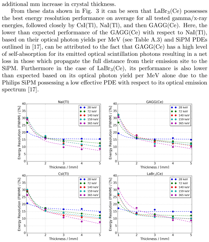
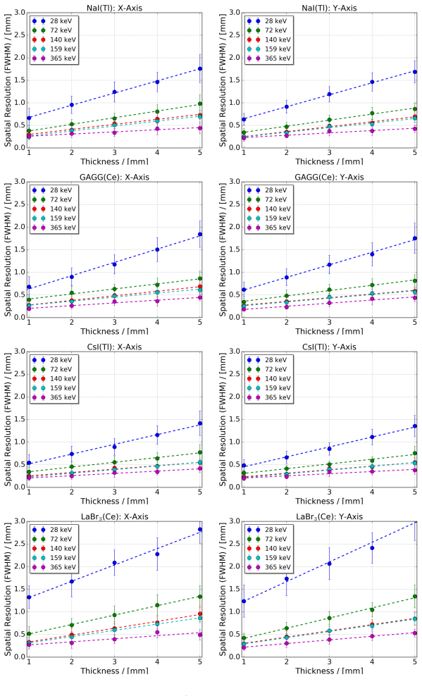
The paper's central claim is that a usable SPECT detector can be built from a thin monolithic scintillator directly bonded to a four-side buttable digital SiPM, but only within a narrow design window: for all four materials tested—NaI(Tl), GAGG(Ce), CsI(Tl), and LaBr3(Ce)—crystals must be 4 to 5 mm thick to keep energy resolution, photoelectric absorption, timing, and spatial resolution simultaneously acceptable. Below that floor, performance degrades sharply because material-specific fluorescence x-rays created by photoelectric absorption escape the crystal and distort the photopeak. The paper further argues that, considering energy and spatial resolution alongside magnetic-resonance compatibility, hygroscopy, and cost, CsI(Tl) is the best overall material for a tileable detector, with GAGG(Ce) and NaI(Tl) trailing on MRI compatibility or moisture sensitivity and LaBr3(Ce) offering the best energy resolution but at high cost, poorer spatial resolution, and strong hygroscopy. At 140 keV with a 5 mm crystal and a truncated centre-of-gravity readout, the simulation gives CsI(Tl) a spatial resolution of 0.55 mm FWHM and an energy resolution of 10.6% FWHM.
Load-bearing premise
The ranking rests on the modelled digital SiPM's electronic response—its photon-detection efficiency, one-trigger-per-diode behaviour, dark-count rate, trigger logic, and integration time—faithfully reproducing the real sensor; if that response model is inaccurate, the simulated energy and spatial resolution values, and possibly the material ordering, would change.
Editorial extensions
If this is right
- Prototyping effort for this class of SPECT detector can be limited to 4–5 mm crystals; thinner monolithic layers will not meet energy and spatial resolution requirements with this type of digital SiPM.
- For combined SPECT/MRI, CsI(Tl) becomes the default candidate even though GAGG(Ce) has slightly higher gamma absorption, because the gadolinium in GAGG makes it unsuitable inside a magnetic field.
- LaBr3(Ce) is a niche choice: best energy resolution and fastest timing, but the largest spatial resolution, highest cost, and strongest hygroscopy of the four materials.
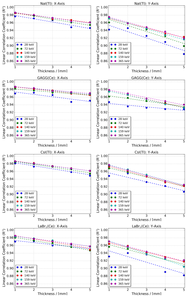
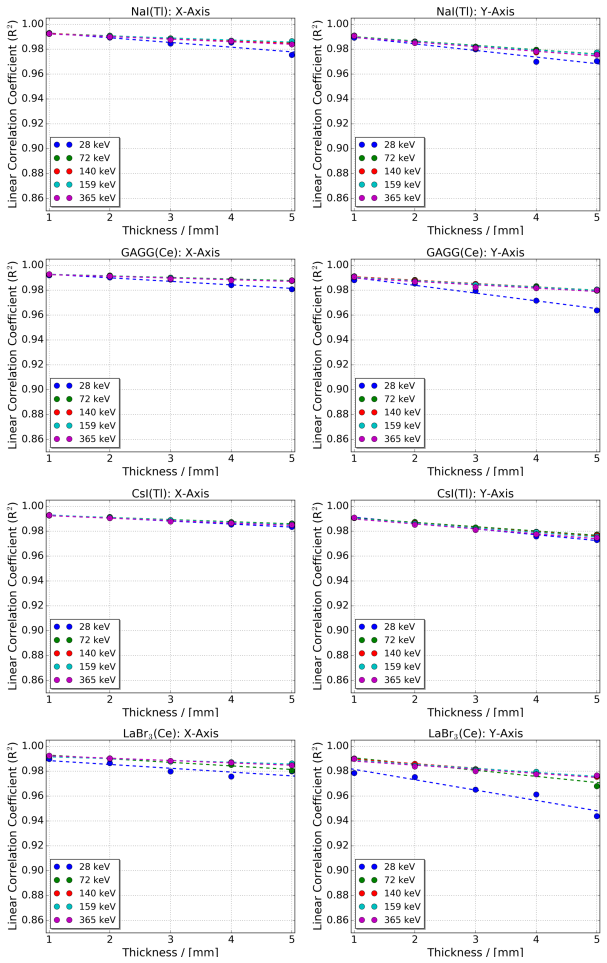
- The truncated centre-of-gravity readout with $\alpha=0.02$ improves spatial linearity across all materials, but it degrades spatial resolution for 28 keV photons in crystals thicker than 3 mm, so the truncation setting should be tuned per energy.
Reading between the lines
- A direct continuation would be to use the same simulation chain to optimise the readout electronics—trigger scheme, integration time, and truncation factor—for each isotope, since the reported timing figures suggest these settings interact strongly with scintillator decay time.
- The 4–5 mm floor is likely to shift when the sensor's photon-detection efficiency or SPAD pitch changes, because the floor is set by x-ray escape and light collection rather than by intrinsic material absorption alone; detectors with more efficient light collection might tolerate thinner crystals.
- A testable extension would be to repeat the optimisation for pixelated or depth-of-interaction-encoding crystal geometries, where the centre-of-gravity readout and the material ranking may change because light sharing is deliberately engineered.
Signed reviews
Editorial analysis
A structured set of objections, weighed in public.
Referee Report
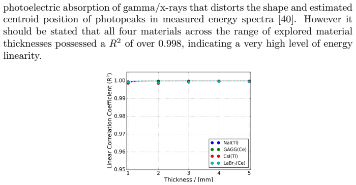
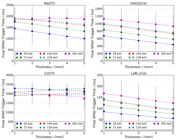
Summary. The paper presents a Geant4-based Monte Carlo study of thin monolithic scintillator detectors coupled to the Philips DPC3200 digital SiPM for SPECT. Four scintillator materials (NaI(Tl), GAGG(Ce), CsI(Tl), LaBr3(Ce)) are simulated at five thicknesses (1–5 mm) for five gamma-ray energies, and are assessed using seven figures of merit including absorption fractions, energy resolution, energy linearity, SPAD trigger timing, and spatial resolution/linearity. The central conclusions are that a 4–5 mm crystal thickness is required for all materials to achieve acceptable energy resolution, sensitivity, and spatial resolution, and that CsI(Tl) is the most promising material when MR compatibility, hygroscopy, and cost are also considered.
Significance. If the simulation model faithfully represents the detector physics, the work provides a useful systematic survey of material/thickness trade-offs for SiPM-based monolithic SPECT detectors, with a practical candidate recommendation (CsI(Tl), 4–5 mm). Strengths include the large statistics (50,000 events per configuration), the detailed treatment of the DPC3200 electronic response (SPAD-level geometry, dark count, trigger scheme, integration time), the inclusion of x-ray escape effects, and the disclosure of material property data in Appendix A. The conclusions are not backed by experimental validation, and one of the central FoMs is built on a restricted event class, which limits the strength of the design recommendation.
major comments (3)
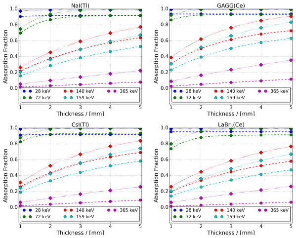
- [§2.3, §3, Table 1] The spatial-resolution FWHM and linearity are computed only for gamma/x-rays that undergo photoelectric absorption on their first interaction. As stated in §2.4, this filter deliberately excludes events that deposit full energy through multiple interactions, yet such events would fall inside a conventional photopeak energy window and contribute to the detector's images. The fraction excluded is not negligible: for the 140 keV data in Table 1, the photoelectric fraction on first interaction (0.582–0.726) is considerably lower than the total absorption fraction (0.719–0.880) for every material, meaning roughly 18–27% of absorbed events are omitted. Because the multi-interaction fraction can vary with crystal thickness and material, the reported spatial-resolution-vs-thickness trade-off may be biased, and the conclusion that a 4–5 mm crystal is required for acceptable spatial resolution (Abstract, §5) overgeneralizes from a restricted event class. The authors should either analyze the full photopeak-window event set or quantitatively justify that the first-interaction photoelectric subset is representative of photopeak imaging performance.
- [§2.3, §3, Table 1] All FoMs are reported as point estimates without statistical uncertainties, even though the simulation uses 50,000 events per configuration and the data are Monte Carlo outputs. Several comparative claims rest on small numerical differences: for example, in Table 1 at 140 keV the energy resolution values for CsI(Tl) (10.6%), GAGG(Ce) (11.5%), and NaI(Tl) (11.0%) differ by about 1%, and the spatial-resolution values of CsI(Tl) (0.551 mm) and GAGG(Ce) (0.639 mm) differ by less than 0.1 mm. Without error bars or a statistical test, the ranking of materials and the thickness thresholds are not shown to be significant. The 'acceptable' 15% energy-resolution threshold in §3 is also introduced without a link to a specific SPECT system requirement. The authors should add uncertainties to all FoM plots and Table 1, and explicitly state the decision criterion used to define 'acceptable'.
- [§2.3] The central predictions are conditional on the five-assumption electronic response model of the DPC3200 SiPM (PDE curve from [17], one-trigger-per-SPAD model, dark count rate, trigger scheme 3, 5125 ns integration time). No experimental validation of this coupled model is provided, and no sensitivity analysis is given for the key parameters (especially the PDE values, which are material-specific effective values of 20.1%, 18.4%, 19.5%, and 9.4%). Because the effective PDE values differ by a factor of ~2 between LaBr3(Ce) and the other materials, a modest change in the PDE curve could materially affect the material ranking and the thickness thresholds. The authors should either provide a comparison with measured data for at least one configuration (e.g., the 5 mm CsI(Tl) prototype that is mentioned as under construction) or perform a parameter sensitivity study over the plausible ranges of PDE and dark-count rate.
minor comments (6)
- [Abstract] There is a typo: 'At present a only small number' should read 'At present only a small number'.
- [§2.4, Eq. (3)] Equation (3) is typeset in a way that obscures the piecewise definition of the truncation; the condition lines are not clearly separated, and a missing brace makes the equation difficult to read. Please reformat this as a proper piecewise function.
- [§3, Figs. 6–9] The term 'irradiation spot spatial resolution' is used, but the FoM is actually the FWHM of the reconstructed position distribution for point irradiations; clearer terminology such as 'point-spread FWHM' would help the reader.
- [Table 1] The abbreviations 'T.A. Fraction' and 'P.A. Fraction' in Table 1 are not self-explanatory; please define them in the caption or in a table note.
- [Discussion] The Discussion makes both 'a minimal crystal thickness of 3 mm is required' and '4 to 5 mm appears to be a viable thickness range'; these statements are compatible but the relationship between them should be stated explicitly to avoid appearing inconsistent.
- [Table 1] The heading 'Hydroscopy' in Table 1 should be 'Hygroscopy'.
Circularity Check
No circular derivation: the optimization is a forward Monte Carlo study whose inputs are literature and manual values; the only mild self-citation is the reuse of the author's prior DPC3200 response model, which is an input assumption rather than a fitted prediction.
full rationale
The paper's derivation chain is a forward Geant4 simulation: geometry, materials, physics lists, and the five-assumption DPC3200 electronic response model are inputs taken from cited literature and the Philips manual, and the seven figures of merit are computed from simulated event data rather than fitted to any target outcome. The central claim that a 4-5 mm crystal thickness is needed follows from observed thresholds in simulated energy resolution, sensitivity, and spatial resolution, and the ranking of CsI(Tl) is then weighted by external material properties such as MR compatibility, hygroscopy, and cost. The only potentially correlated element is the reuse of the author's prior DPC3200 response model from Brown et al. [31], cited in Section 2.3, but this is an input modeling assumption, not a result whose conclusion is encoded in it; it does not make the material/thickness comparison circular. Section 2.4's restriction of the spatial-resolution figure of merit to first-interaction photoelectric events narrows the claim to a subset of events, but this is a limitation about generalizing to actual photopeak events, not a self-referential reduction. No step of the argument equates a prediction with a fit parameter, nor does it import a uniqueness theorem from self-citation. The score of 2 reflects the minor self-citation without load-bearing circularity.
Assumptions & free parameters
free parameters (4)
- Surface roughness (sigma_alpha) =
0.1 degrees
- CoG truncation factor alpha =
0 and 0.02
- Maximum particle step length =
10 micrometers
- Low-energy cutoff =
250 eV
assumptions (5)
- domain assumption Geant4 Option4 EM physics list with atomic de-excitation accurately models photoelectric absorption, fluorescence x-ray production and escape, and electron transport down to 250 eV.
- domain assumption The Philips DPC3200 photosensor electronic response model (five assumptions in Section 2.3) accurately represents the real device's PDE, dark count rate, trigger logic and integration time.
- domain assumption The Unified optical surface model with ground surface roughness of 0.1 degrees and the listed refractive indices and attenuation lengths (Appendix A) are realistic for the simulated materials and interfaces.
- standard math FWHM values calculated assuming Gaussian distributions from the simulated energy and position spectra.
- domain assumption The material data (optical yield, decay time, refractive index, attenuation length) taken from literature are correct for the specific crystal dopings used.
Cite this review
Pith. "Pith review of In-Silico Optimisation of Tileable Philips Digital SiPM Based Thin Monolithic Scintillator Detectors for SPECT Applications." pith.science (2026). https://pith.science/paper/MLAQCVMU
@misc{pith2026190804565,
  author       = {Pith},
  title        = {Pith review of: In-Silico Optimisation of Tileable Philips Digital SiPM Based Thin Monolithic Scintillator Detectors for SPECT Applications},
  year         = {2026},
  howpublished = {\url{https://pith.science/paper/MLAQCVMU}},
  note         = {Machine review of arXiv:1908.04565}
}
abstract
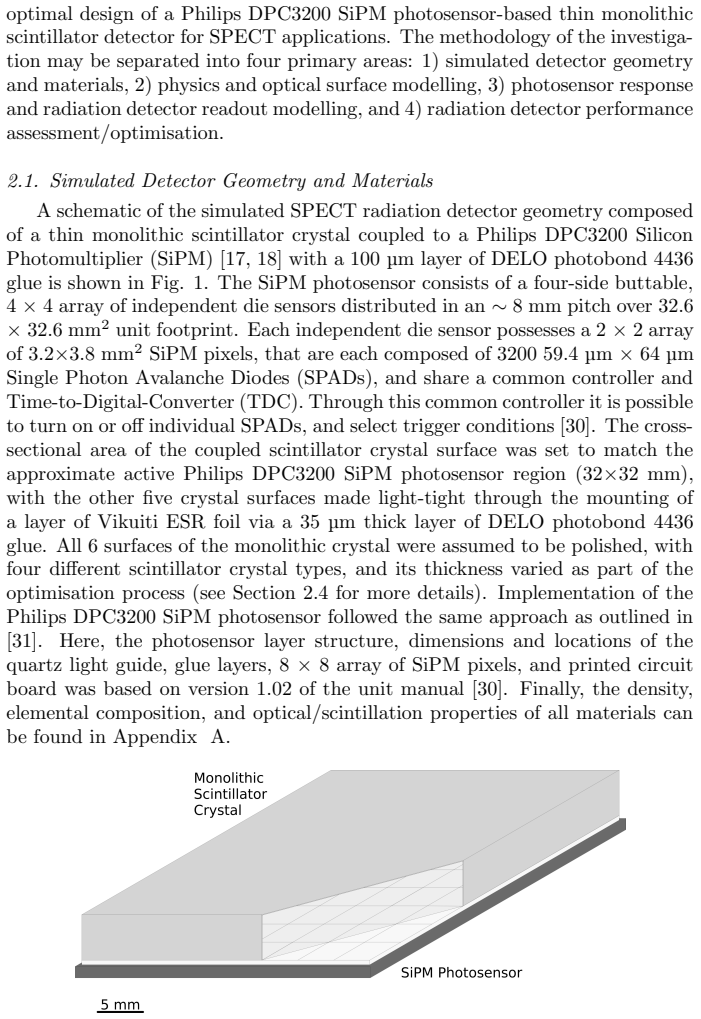
Over the last decade one of the most significant technological advances made in the field of radiation detectors for nuclear medicine was the development of Silicon Photomultipler (SiPM) sensors. At present a only small number of SiPM based radiation detectors for Single Photon Emission Computed Tomography (SPECT) applications have been explored, and even fewer experimental prototypes developed. An in-silico investigation into the optimal design of a Philips DPC3200 SiPM photosensor-based thin monolithic scintillator detector for SPECT applications was undertaken using the Monte Carlo radiation transport modelling toolkit Geant4 version 10.5. The performance of the 20 different SPECT radiation detector configurations, 4 scintillator materials (NaI(Tl), GAGG(Ce), CsI(Tl) and LaBr$_{3}$(Ce)) and 5 thicknesses (1 to 5 mm), were determined through the use of seven figures of merit. It was found that a crystal thickness range of 4 to 5 mm was required for all four materials to ensure acceptable energy resolution, sensitivity and spatial resolution performance with the Philips DPC3200 SiPM. Any thinner than this and the performance of all four materials was found to degrade rapidly due to a high probability of material specific fluorescence x-ray escape after incident gamma/x-ray photoelectric absorption. When factoring in each material's magnetic resonance imaging compatibility, hygroscopy, and cost, it was found that CsI(Tl) represents the most promising material to construct tileable Philips digital SiPM based thin monolithic scintillator detectors for SPECT applications.
Figures
Figures from the paper (6 more)

Reference graph
Works this paper leans on
-
[17]
Frach T., Prescher G., Degenhardt C., de Gruyter R., Schmitz A. and Bal- lizany R. The digital silicon photomultiplier: Principle of operation and in- trinsic detector performance, 2009 IEEE Nuclear Science Symposium Con- ference Record (NSS/MIC): 1959-1965 (2009)
work page 2009
-
[1]
Kupinski M. A. and Barrett H. H. Small-Animal SPECT Imaging, Springer Science 2005
work page 2005
-
[2]
Brown J. M. C., Gillam J. E., Paganin D. M. and Dimmock M. R.Laplacian erosion: an image deblurring technique for multi-plane gamma-cameras , IEEE Transactions on Nuclear Science 60(5): 3333-3342 (2013)
work page 2013
-
[3]
Cherry S. R., Sorenson J. A. and Phelps M. E. Physics in Nuclear Medicine, Elsevier Science 2003
work page 2003
-
[4]
Bushberg J. T. and Boone J. M. The essential physics of medical imaging , Lippincott, Williams & Wilkins (2011)
work page 2011
-
[5]
Recent developments in PET detector technology , Physics in Medicine & Biology 53(17): R287 (2008)
Lewellen TK. Recent developments in PET detector technology , Physics in Medicine & Biology 53(17): R287 (2008)
work page 2008
-
[6]
Schaart D. R., Charbon E., Frach T. and Schulz V. Advances in digital SiPMs and their application in biomedical imaging , Nuclear Instruments and Methods in Physics Research Section A 809: 31-52 (2016)
work page 2016
-
[7]
Bisogni M. G., Del Guerra A. and Belcari. N. Medical applications of silicon photomultipliers, Nuclear Instruments and Methods in Physics Research Section A 926: 118-128 (2018)
work page 2018
Show all 49 references
-
[8]
S., Catana C., Swann B
Judenhofer M. S., Catana C., Swann B. K., Siegel S. B., Jung W. I., Nutt R. E., Cherry S. R., Claussen C. D. and Pichler B. J. PET/MR im- ages acquired with a compact MR-compatible PET detector in a 7-T magnet, Radiology 244(3): 807-814 (2007)
2007
-
[9]
Schlemmer H. P. W., Pichler B. J., Schmand M., Burbar Z., Michel C., Ladebeck R., Jattke K., Townsend D., Nahmias C., Jacob P. K. and Heiss W. D. Simultaneous MR/PET imaging of the human brain: feasi- bility study, Radiology 248(3): 1028-1035 (2008). 19
2008
-
[10]
F., Judenhofer M
Wehrl H. F., Judenhofer M. S., Wiehr S. and Pichler B. J. Pre-clinical PET/MR: technological advances and new perspectives in biomedical re- search, European Journal of Nuclear Medicine and Molecular Imaging 36: 56-68 (2009)
2009
-
[11]
G., Schwaiger M
Delso G., F urst S., Jakoby B., Ladebeck R., Ganter C., Nekolla S. G., Schwaiger M. and Ziegler S. I. Performance measurements of the Siemens mMR integrated whole-body PET/MR scanner, Journal of Nuclear Medicine 52(12): 1914-1922 (2011)
2011
-
[12]
Weissler B. et al. A digital preclinical PET/MRI insert and initial results , IEEE Transactions on Medical Imaging 34(11): 2258-2270 (2015)
2015
-
[13]
Gonz´ alez A. J. et al.The MINDView brain PET detector, feasibility study based on SiPM arrays , Nuclear Instruments and Methods in Physics Re- search Section A 818: 82-90 (2016)
2016
-
[14]
Benlloch J. M. et al. The MINDVIEW project: First results European Psychiatry 50:21-27 (2018)
2018
-
[15]
J., S´ anchez F., Benlloch J
Gonz´ alez A. J., S´ anchez F., Benlloch J. M.Organ-dedicated molecular imag- ing systems, IEEE Transactions on Radiation and Plasma Medical Sciences 2(5): 388-403 (2018)
2018
-
[16]
HYPMED Consortium, http://www.hypmed.eu/ (2019)
2019
-
[18]
and Zwaans B
Frach T., Prescher G., Degenhardt C. and Zwaans B. The digital sili- con photomultiplier—System architecture and performance evaluation, 2010 IEEE Nuclear Science Symposium Conference Record (NSS/MIC): 1722- 1727 (2010)
2010
-
[19]
W., Korevaar M
Heemskerk J. W., Korevaar M. A., Huizenga J., Kreuger R., Schaart D. R., Goorden M. C. and Beekman F. J. An enhanced high-resolution EMCCD- based gamma camera using SiPM side detection , Physics in Medicine & Biology 55(22): 6773-6784 (2010)
2010
-
[20]
V., Loudos G
Georgiou M., Borghi G., Spirou S. V., Loudos G. and Schaart D. R. First performance tests of a digital photon counter (DPC) array coupled to a CsI (Tl) crystal matrix for potential use in SPECT , Physics in Medicine & Biology 59(10): 2415-2430 (2014)
2014
-
[21]
and Rieger J.Experimental evaluation of a SiPM-based scintillation detector for MR-compatible SPECT systems , IEEE Transactions on Nuclear Science 62(5): 2122-2128 (2015)
Busca P., Occhipinti M., Trigilio P., Cozzi G., Fiorini C., Piemonte C., Ferri A., Gola A., Nagy K., B ukki T. and Rieger J.Experimental evaluation of a SiPM-based scintillation detector for MR-compatible SPECT systems , IEEE Transactions on Nuclear Science 62(5): 2122-2128 (2015). 20
2015
-
[22]
and Loudos G
David S., Georgiou M., Fysikopoulos E. and Loudos G. Evaluation of a SiPM array coupled to a Gd 3Al2Ga3O12:Ce (GAGG:Ce) discrete scintilla- tor, Physica Medica 31(7): 763-766 (2015)
2015
-
[23]
Busca P. et al. Simulation of the expected performance of INSERT: A new multi-modality SPECT/MRI system for preclinical and clinical imaging , Nuclear Instruments and Methods in Physics Research Section A 734: 141- 146 (2014)
2014
-
[24]
Hutton B. F. et. al Development of clinical simultaneous SPECT/MRI, The British Journal of Radiology 91: 20160690 (2018)
2018
-
[25]
J., Erlandsson K., Nagy K., Czeller M., T¨ olgyesi B., Nyitrai Z., Savi A., van Mullekom, P
Carminati M., D’Adda I., Morahan A. J., Erlandsson K., Nagy K., Czeller M., T¨ olgyesi B., Nyitrai Z., Savi A., van Mullekom, P. and Hutton B. F. Clinical SiPM-Based MRI-Compatible SPECT: Preliminary Characterization, IEEE Transactions on Radiation and Plasma Medical Sciences:...
2019
-
[26]
and Korzhik M
Lecoq P., Gektin A. and Korzhik M. Inorganic scintillators for detector systems: physical principles and crystal engineering , Springer (2016)
2016
-
[27]
Agostinelli S. et al. Geant4-a simulation toolkit , Nuclear Instruments and Methods in Physics Research Section A 506(3): 250-303 (2003)
2003
-
[28]
Allison J. et al. Geant4 developments and applications , IEEE Transactions on Nuclear Science 53(1): 270-278 (2006)
2006
-
[29]
Allison J. et al. Recent developments in Geant4 , Nuclear Instruments and Methods in Physics Research Section A 835: 186-225 (2016)
2016
-
[30]
Module-TEK User Manual, Philips Digital Photon Counting (2016)
2016
-
[31]
Brown J. M. C., Brunner S. E. and Schaart D. R. A High Count-Rate and Depth-of-Interaction Resolving Single Layered One-Side Readout Pixelated Scintillator Crystal Array for PET Applications , IEEE Transactions on Radiation and Plasma Medical Sciences 4(3): 361-370 (2020)
2020
-
[32]
and Moisan C
Levin A. and Moisan C. A more physical approach to model the surface treatment of scintillation counters and its implementation into DETECT , 1996 IEEE Nuclear Science Symposium Conference Record 2: 702-706 (1996)
1996
-
[33]
GEANT4 Collaboration, GEANT4 Physics Reference Manual-Version 10.5, https://geant4.web.cern.ch (2019)
2019
-
[34]
J., Schaart D
Van der Laan D. J., Schaart D. R., Maas M. C., Beekman F. J., Bruyn- donckx P. and van Eijk C.W. Optical simulation of monolithic scintillator detectors using GATE/GEANT4 , Physics in Medicine & Biology 55(6): 1659-1675 (2010). 21
2010
-
[35]
and Isaksson M
Nilsson J., Cuplov V. and Isaksson M. Identifying key surface parameters for optical photon transport in GEANT4/GATE simulations , Applied Ra- diation and Isotopes 103: 15-24 (2015)
2015
-
[36]
Steinbach D., Majewski S., Williams M., Kross B., Weisenberger A. G. and Wojcik R. Development of a small field of view scintimammography camera based on a YAP crystal array and a position sensitive PMT . 1996 IEEE Nuclear Science Symposium Conference Record 2: 1251-1256) (1996)
1996
-
[37]
and Weisenberger A
Wojcik R., Majewski S., Kross B., Popov V. and Weisenberger A. G. Op- timized readout of small gamma cameras for high resolution single gamma and positron emission imaging , In 2001 IEEE Nuclear Science Symposium Conference Record : 1821-1825 (2001)
2001
-
[38]
V., Faber T
Garcia E. V., Faber T. L. and Esteves F. P. Cardiac dedicated ultrafast SPECT cameras: new designs and clinical implications , Journal of Nuclear Medicine 52(2): 210-217 (2011)
2011
-
[39]
J., Hubbell J
Berger M. J., Hubbell J. H., Seltzer S. M., Chang J., Coursey J. S., Suku- mar R., Zucker D. S., and Olsen K. XCOM: Photon Cross Section Database (version 1.5), [Online] Available: http://physics.nist.gov/xcom (2019)
2019
-
[40]
Practical gamma-ray spectroscopy, John Wiley & Sons (2011)
Gilmore G. Practical gamma-ray spectroscopy, John Wiley & Sons (2011)
2011
-
[41]
V., Bergholt L., Guttormsen M., Taylor J
Avdeichikov V. V., Bergholt L., Guttormsen M., Taylor J. E., Wester- berg L., Jakobsson B., Klamra W. and Murin, Y.A.Light output and energy resolution of CsI, YAG, GSO, BGO and LSO scintillators for light ions , Nuclear Instruments and Methods in Physics Research Section A 34...
1994
-
[42]
and Senda M
Yamamoto S., Kuroda K. and Senda M. Scintillator selection for MR- compatible gamma detectors. IEEE Transactions on Nuclear Science 50(5): 1683-1685 (2003)
2003
-
[43]
2016, Monte-Carlo simulation of a new ultra-fast gamma detector design in Geant4
Dachs F. 2016, Monte-Carlo simulation of a new ultra-fast gamma detector design in Geant4 . Masters’ Dissertation, Vienna University of Technology (Vienna, Austria)
2016
-
[44]
3M Vikuiti Enhanced Spectral Reflector Datasheet, http://www.3m.com (2019)
2019
-
[45]
Philipp H. R. and Taft E. A. Optical constants of silicon in the region 1 to 10 eV, Physical Review 120(1): 37-38 (1960)
1960
-
[46]
and Zhu R
Mao R., Zhang L. and Zhu R. Y. Optical and scintillation properties of in- organic scintillators in high energy physics , IEEE Transactions on Nuclear Science 55(4): 2425-2431 (2008). 22
2008
-
[47]
and Usuki Y
Kobayashi M., Tamagawa Y., Tomita S., Yamamoto A., Ogawa I. and Usuki Y. Significantly different pulse shapes for γ-and α-rays in Gd 3Al2Ga33O12:Ce3+ scintillating crystals , Nuclear Instruments and Methods in Physics Research Section A 694: 91-94 (2012)
2012
-
[48]
W., Higgins W
Glodo J., Moses W. W., Higgins W. M., Van Loef E. V. D., Wong P., Derenzo S. E., Weber M. J. and Shah K. S. Effects of Ce concentration on scintillation properties of LaBr 3(Ce), IEEE Transactions on Nuclear Science 52(5): 1805-1808 (2005)
2005
-
[49]
and Schaart D
van Dam H T., Seifert S., Drozdowski W., Dorenbos P. and Schaart D. R. Optical Absorption Length, Scattering Length, and Refractive Index of LaBr3:Ce3+, IEEE Transactions on Nuclear Science 59(3): 656-664 (2012). 23 Optical Material Density Elemental Refractive Reflectivity / R...
2012
Reviewed August 14, 2026 · model on record in the stance chip above.
Discussion (0). Continue with ORCID to comment.