REVIEW 3 major objections 6 minor 24 references
High-Speed Phase-Only Spatial Light Modulators with Two-Dimensional Tunable Microcavity Arrays
T0 review · 3 major / 6 minor · reviewed 2026-08-14 · deepseek-v4-flash
Pith's one-line read A two-dimensional array of voltage-tuned microcavities can provide phase-only spatial light modulation at gigahertz speeds, with a simulated π phase shift at 9.3 V and reflectance above 90 percent.
desk verdict A credible simulation-based optical design for a phase-only BTO microcavity SLM array; the GHz speed claim is unsupported without electrical analysis. read the letter →
The pith
A machine-rendered reading of the paper's core claim, the machinery that carries it, and where it could break.
The reading
What carries the argument
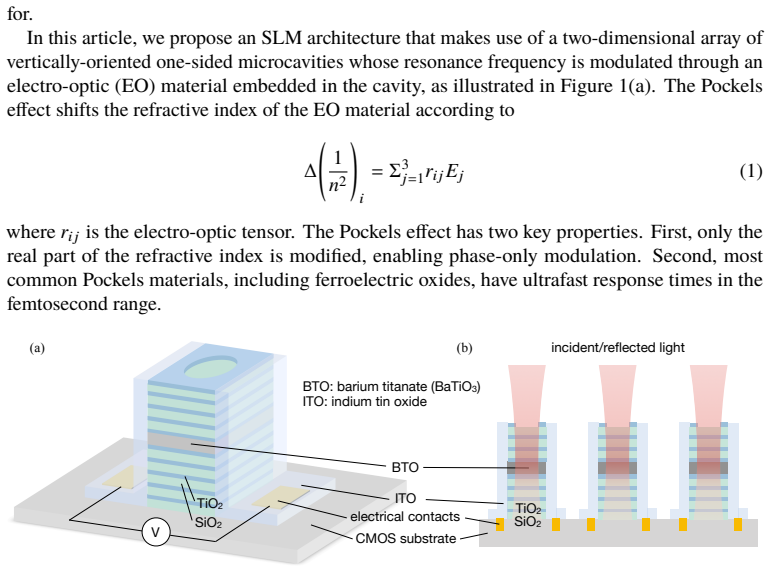
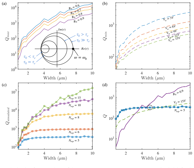
The central object is the one-sided asymmetric Fabry-Perot microcavity, analyzed with temporal coupled-mode theory. The complex reflection coefficient r(ω) depends on the internal loss rate 1/τ0 and the cavity–free-space coupling rate 1/τe; operating with 1/τe > 1/τ0 (over-coupled regime) lets the detuning induced by the electro-optic index change sweep the reflection phase through 2π while keeping the amplitude near unity. The design method places an upper bound on loaded Q from the reflectance requirement and a lower bound from the voltage-limited detuning, then finds a micropost geometry satisfying both. Perturbation theory relates the index change to the resonance shift through the energy fraction stored in the BTO layer, and the crystal-orientation analysis maps the Pockels tensor onto the applied-field direction to maximize the effective coefficient.
What would settle it
Fabricate a single pixel with the reported geometry (5 µm pillar, 5 top DBR pairs, BTO layer with c-axis at 45 degrees to the field), measure the reflection phase and amplitude versus applied DC voltage, and record the small-signal modulation response. If Vπ exceeds ~10 V, if the reflectance drops below 0.9 across the phase range, or if the 3 dB bandwidth falls well below 1 GHz due to RC limits, the central claims are contradicted.
Extended reading notes
Core claim
The central claim is that phase-only modulation at gigahertz speed can be obtained from a 2D array of vertical microcavities whose resonance is tuned by the Pockels effect in BTO. Using temporal coupled-mode theory, the authors show that a one-sided resonator in the over-coupled regime can provide a full 0-to-2π reflection phase change with nearly constant amplitude, and that the required loaded quality factor is bounded both above (by the desired on-resonance reflectance) and below (by the voltage needed to reach π phase). The optimized pixel, a 5-µm-wide micropost with five top DBR pairs, is simulated to give Vπ = 9.3 V at R > 0.9, matching the bounds. The authors also determine the optimal crystalline orientation of BTO relative to the in-plane applied field, finding an effective Pockels coefficient of 872 pm/V at about 45 degrees for multi-domain films. Array simulations show continuous beam steering and varifocal focusing, with no undeflected ghost orders.
Load-bearing premise
The gigahertz modulation speed is assumed to be set by the sub-picosecond Pockels response of BTO, but the paper does not analyze whether the electrical addressing path—CMOS drivers, metal interconnects, ITO electrodes, and pixel capacitance—can actually refresh an array at gigahertz rates.
Editorial extensions
If this is right
- A single phase-shifter element can provide full 0-to-2π phase control with reflectance amplitude above 0.9 at a drive voltage below 15 V, with Vπ = 9.3 V.
- A 20x20 array with 5.2 µm pitch can continuously steer a reflected beam over a wide angular range without residual undeflected (ghost) beam, because the modulation is phase-only.
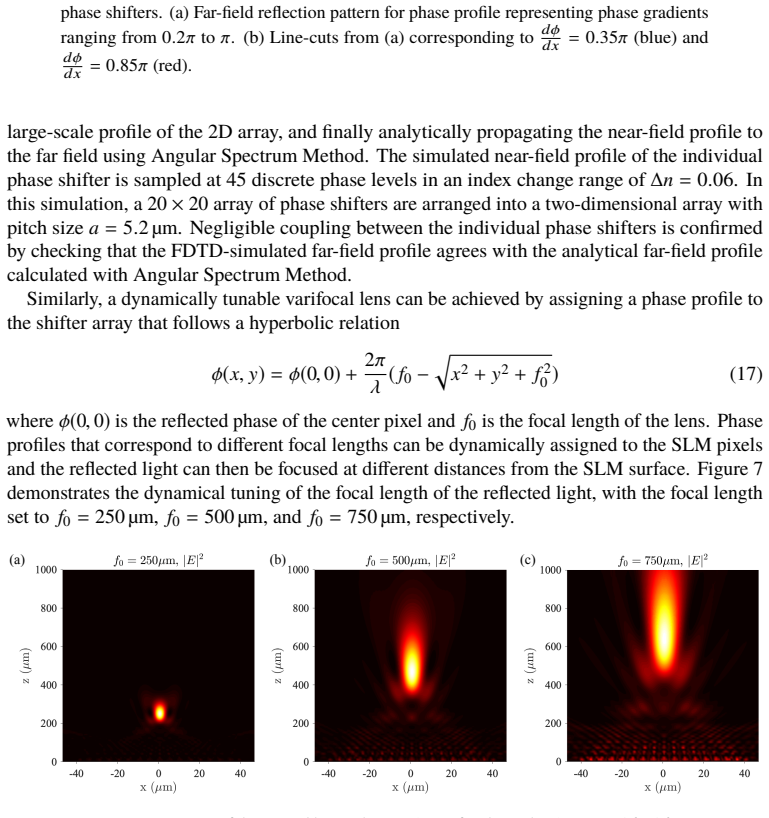
- A 16x16 array implementing a hyperbolic phase profile acts as a varifocal lens, focusing reflected light at distances set by the phase pattern.
- The Pockels effect in BTO gives sub-picosecond material response, so the architecture is projected to support modulation speeds beyond 1 GHz if electrical addressing keeps up.
- The design methodology (Q bounds, orientation optimization) extends to other specifications such as amplitude modulation.
Reading between the lines
- The array-level simulation samples single-pixel near-fields and propagates them analytically; if inter-pixel coupling becomes significant at smaller pitch or larger fill factor, the assumed periodicity could break, which the paper's negligible-coupling check for the specific 5.2 µm pitch does not rule out.
- The GHz speed claim rests on the material response, not on the electrical path; a quick RC estimate using the ITO sheet resistance and pixel capacitance would indicate whether CMOS addressing can actually refresh the array at GHz rates, a test the paper does not perform.
- The same over-coupled microcavity design could be adapted to other electro-optic or nonlinear materials where the tuning mechanism differs, potentially trading voltage for speed or wavelength range.
- If fabricated, this pixel geometry could also serve as a building block for reconfigurable metasurfaces, since the sub-wavelength-scale microposts form a phased array with voltage-tunable phase.
Signed reviews
Editorial analysis
A structured set of objections, weighed in public.
Referee Report
Summary. The paper proposes a two-dimensional array of vertical one-sided microcavities with a barium-titanate (BTO) active layer as a phase-only spatial light modulator (SLM). Using temporal coupled-mode theory (TCMT) bounds and FDTD simulations, the authors design a pixel with a 5 μm post width and five top DBR pairs that achieves a simulated π phase shift at Vπ = 9.3 V while maintaining reflectance R > 0.9 at 1550 nm. They then illustrate dynamic 2D beam steering and a varifocal focusing function by applying phase profiles to small arrays, and the abstract and conclusion claim modulation speeds in excess of 1 GHz based on the electro-optic response of BTO.
Significance. The optical phase-shifter design is credible and useful. The use of measured BTO electro-optic coefficients, the independent FDTD validation of the analytic quality-factor bounds, and the explicit, falsifiable prediction of Vπ = 9.3 V with R > 0.9 are strengths. The architecture could be a significant advance over slow LCOS-based SLMs if the speed claim is supported by electrical analysis. As written, however, the headline speed claim rests only on the femtosecond Pockels response and an unrelated 65 GHz waveguide modulator, so the paper's most important claim is not yet substantiated.
major comments (3)
- [Abstract and Section 5] The claim of "high speed in excess of GHz" is not supported by any electrical analysis. The pixel is an electrically addressed parallel-plate capacitor with ITO contacts on a CMOS substrate, but no capacitance, series resistance, RC time constant, driver bandwidth, or array refresh-rate analysis appears in Sections 1–5. The 65 GHz waveguide modulator of Ref. [17] is not evidence for a dense free-space pixel array. Please add an electrical model of a single pixel and of the array addressing, or explicitly limit the speed claim to the material Pockels response with a quantitative caveat.
- [Section 4] The statement that "Negligible coupling between the individual phase shifters is confirmed by checking that the FDTD-simulated far-field profile agrees with the analytical far-field profile calculated with Angular Spectrum Method" is ambiguous: if the FDTD simulation is of a single pixel, the comparison tests only the propagation model and not inter-pixel coupling; if it is of a multi-pixel array, that should be stated explicitly. Inter-pixel coupling at 5.2 μm pitch with 5 μm posts could affect the phase patterns used in the beam-steering and focusing demonstrations.
- [Section 2.1, Eq. (2)] The denominator of Eq. (2) is printed as (1/τ_e^2 + 1/τ_0^2) + (ω0 − ω)^2, which is inconsistent with the standard one-sided TCMT pole (1/τ_e + 1/τ_0)^2 + (ω0 − ω)^2 and with the expressions that follow in Eqs. (3), (7), and (9). This appears to be a typographical error, but it should be corrected because the analytic Q bounds in Section 2.1 are presented as the design methodology.
minor comments (6)
- [Section 2.3, after Eq. (13)] The sentence about deriving n_y′ and r_y′z′ from the y′z′ term is vague; please give the explicit formulae or a reference.
- [Figure 3(b)] The caption should state that the vertical axis is phase (in units of π) and reflectance, and should define the horizontal axis range and the location of Vπ.
- [Section 2.2] The claim of "full 0 to 2π phase control" should be accompanied by the voltage or Δn range needed to span 2π, since the quantitative abstract claim is only for a π phase shift.
- [Table 1] The parameter d is labeled "thickness of the cavity layer 678 nm"; please state that this is the vertical BTO layer thickness and identify the horizontal electrode gap used for the voltage-to-field conversion (appears to be D = 5 μm) so that the Vπ calculation is reproducible.
- [Section 1, last paragraph] The statement that reflection through a 1 μm BTO film gives Δφ ≈ 0.15π would benefit from a brief derivation so the reader can verify the need for cavity enhancement.
- [Simulation methodology, Section 2.2] The description of the FDTD simulation should state the specific solver version and a brief note on meshing or convergence criteria.
Circularity Check
No significant circularity: the central phase-shift design is derived from external BTO material parameters, TCMT/perturbation theory, and independent FDTD simulation.
full rationale
The paper's central claim is that an optimized one-sided microcavity with a BTO electro-optic layer achieves a pi phase shift under 9.3 V with nearly constant reflectance. The derivation chain starts from the Pockels effect in Eq. (1), with BTO coefficients r42 = 923 pm/V, r33 = 342 pm/V, r13 = -63 pm/V and refractive indices taken from the external experimental literature (Ref. [17], Abel et al.). The reflection model Eq. (2) is standard TCMT, and the loaded-Q bounds Eqs. (4) and (9) follow analytically from TCMT and perturbation theory. The intrinsic Q and the energy fraction U_BTO/U_tot are obtained from an auxiliary simulation with perfectly reflecting mirrors, not from the target V_pi value. The parameter sweep over D and N_top selects a design satisfying R0 > 0.9 and V_pi < 15 V; the subsequent full FDTD simulation gives V_pi = 9.3 V and is compared with the analytic prediction, so the simulated result is not used to define the analytic bounds. The effective Pockels coefficient rz'z' = 872 pm/V is derived analytically from the electro-optic tensor and the crystal orientation in Section 2.3, using measured tensor components; it is not fitted to the final V_pi. Self-citations (Refs. [5] and [8]) appear only in application discussions and are not load-bearing for the phase-shift or speed derivations. The high-speed claim is an extrapolation from BTO's femtosecond Pockels response and the external 65 GHz BTO modulator demonstration in Ref. [17]; while the array-level electrical addressing path is not analyzed and the speed claim may be unsupported, this is a correctness/evidence gap rather than a circular reduction. No fitted input is renamed as a prediction, and no derivation step is equivalent to its own input by construction. A typographical inconsistency in the denominator of Eq. (2) does not create circularity.
Assumptions & free parameters
free parameters (3)
- Micropost width D =
5 µm
- Number of top DBR pairs Ntop =
5
- BTO c-axis angle θ =
45° (multi-domain assumption)
assumptions (4)
- domain assumption Temporal coupled-mode theory expression for the reflection coefficient of a one-sided resonator, Eq. (2).
- domain assumption The ITO/BTO/ITO structure behaves as an ideal parallel-plate capacitor with a uniform horizontal electric field in the BTO layer.
- domain assumption Multi-domain BTO films contain equal populations of domains oriented in the two perpendicular in-plane directions.
- ad hoc to paper The Pockels response time of BTO, not the electrical drive network, sets the SLM modulation speed.
Cite this review
Pith. "Pith review of High-Speed Phase-Only Spatial Light Modulators with Two-Dimensional Tunable Microcavity Arrays." pith.science (2026). https://pith.science/paper/XHUJEBX7
@misc{pith2026190806495,
  author       = {Pith},
  title        = {Pith review of: High-Speed Phase-Only Spatial Light Modulators with Two-Dimensional Tunable Microcavity Arrays},
  year         = {2026},
  howpublished = {\url{https://pith.science/paper/XHUJEBX7}},
  note         = {Machine review of arXiv:1908.06495}
}
read the original abstract
Spatial light modulators (SLMs) are central to numerous applications ranging from high-speed displays to adaptive optics, structured illumination microscopy, and holography. After decades of advances, SLM arrays based on liquid crystals can now reach large pixel counts exceeding 10^6 with phase-only modulation with a pixel pitch of less than 10 {\mu}m and reflectance around 75%. However, the rather slow modulation speed in such SLMs (below hundreds of Hz) presents limitations for many applications. Here we propose an SLM architecture that can achieve high pixel count with high-resolution phase-only modulation at high speed in excess of GHz. The architecture consists of a tunable two-dimensional array of vertically oriented, one-sided microcavities that are tuned through an electro-optic material such as barium titanate (BTO). We calculate that the optimized microcavity design achieves a {\pi} phase shift under an applied bias voltage below 10 V, while maintaining nearly constant reflection amplitude. As two model applications, we consider high-speed 2D beam steering as well as beam forming. The outlined design methodology could also benefit future design of spatial light modulators with other specifications (for example amplitude modulators). This high-speed SLM architecture promises a wide range of new applications ranging from fully tunable metasurfaces to optical computing accelerators, high-speed interconnects, true 2D phased array beam steering, and quantum computing with cold atom arrays.
Figures

Figures from the paper (4 more)


Reference graph
Works this paper leans on
-
[17]
Large pockels effect in micro-and nanostructured barium titanate integrated on silicon,
S. Abel, F. Eltes, J. E. Ortmann, A. Messner, P. Castera, T. Wagner, D. Urbonas, A. Rosa, A. M. Gutierrez, D. Tulli et al., “Large pockels effect in micro-and nanostructured barium titanate integrated on silicon,” Nat. materials18, 42 (2019)
work page 2019
-
[1]
Lidar: Mapping the world in 3d,
B. Schwarz, “Lidar: Mapping the world in 3d,” Nat. Photonics4, 429 (2010)
work page 2010
-
[2]
Laser beam steering and tracking using a liquid crystal spatial light modulator,
E. Haellstig, J. Stigwall, M. Lindgren, and L. Sjoqvist, “Laser beam steering and tracking using a liquid crystal spatial light modulator,” inLaser Systems Technology,vol. 5087 (International Society for Optics and Photonics, 2003), pp. 13–23
work page 2003
-
[3]
Creation and detection of optical modes with spatial light modulators,
A. Forbes, A. Dudley, and M. McLaren, “Creation and detection of optical modes with spatial light modulators,” Adv. Opt. Photonics8, 200–227 (2016)
work page 2016
-
[4]
Terahertz compressive imaging with metamaterial spatial light modulators,
C. M. Watts, D. Shrekenhamer, J. Montoya, G. Lipworth, J. Hunt, T. Sleasman, S. Krishna, D. R. Smith, and W. J. Padilla, “Terahertz compressive imaging with metamaterial spatial light modulators,” Nat. Photonics8, 605 (2014)
work page 2014
-
[5]
Large-scale optical neural networks based on photoelectric multiplication,
R. Hamerly, L. Bernstein, A. Sludds, M. Soljačić, and D. Englund, “Large-scale optical neural networks based on photoelectric multiplication,” Phys. Rev. X9, 021032 (2019)
work page 2019
-
[6]
All-optical machine learning using diffractive deep neural networks,
X. Lin, Y. Rivenson, N. T. Yardimci, M. Veli, Y. Luo, M. Jarrahi, and A. Ozcan, “All-optical machine learning using diffractive deep neural networks,” Science361, 1004–1008 (2018)
work page 2018
-
[7]
Single-atom trapping in holographic 2d arrays of microtraps with arbitrary geometries,
F. Nogrette, H. Labuhn, S. Ravets, D. Barredo, L. Béguin, A. Vernier, T. Lahaye, and A. Browaeys, “Single-atom trapping in holographic 2d arrays of microtraps with arbitrary geometries,” Phys. Rev. X4, 021034 (2014)
work page 2014
Show all 24 references
-
[8]
Large-scale uniform optical focus array generation with a phase spatial light modulator,
D. Kim, A. Keesling, A. Omran, H. Levine, H. Bernien, M. Greiner, M. D. Lukin, and D. R. Englund, “Large-scale uniform optical focus array generation with a phase spatial light modulator,” Opt. letters44, 3178–3181 (2019)
2019
-
[9]
Fundamentals of phase-only liquid crystal on silicon (lcos) devices,
Z. Zhang, Z. You, and D. Chu, “Fundamentals of phase-only liquid crystal on silicon (lcos) devices,” Light. Sci. & Appl. 3, e213 (2014)
2014
-
[10]
Free space adaptive optical interconnect at 1.25 gb/s, with beam steering using a ferroelectric liquid-crystal slm,
C. J. Henderson, D. G. Leyva, and T. D. Wilkinson, “Free space adaptive optical interconnect at 1.25 gb/s, with beam steering using a ferroelectric liquid-crystal slm,” J. Light. Technol.24, 1989–1997 (2006)
2006
-
[11]
Emerging digital micromirror device (dmd) applications,
D. Dudley, W. M. Duncan, and J. Slaughter, “Emerging digital micromirror device (dmd) applications,” inMOEMS display and imaging systems,vol. 4985 (International Society for Optics and Photonics, 2003), pp. 14–26
2003
-
[12]
Development of a high-speed high-fill-factor phase-only spatial light modulator,
V. Shrauger and C. Warde, “Development of a high-speed high-fill-factor phase-only spatial light modulator,” in DiffractiveandHolographicTechnologiesforIntegratedPhotonicSystems, vol.4291(InternationalSocietyforOptics and Photonics, 2001), pp. 101–109
2001
-
[13]
Memsreliabilityfromafailuremechanismsperspective,
W.M.VanSpengen,“Memsreliabilityfromafailuremechanismsperspective,”Microelectron.Reliab. 43,1049–1060 (2003)
2003
-
[14]
Silicon spatial light modulator,
R. A. Soref, “Silicon spatial light modulator,” (1992). US Patent 5,157,538
1992
-
[15]
Gate-tunable conducting oxide metasurfaces,
Y.-W. Huang, H. W. H. Lee, R. Sokhoyan, R. A. Pala, K. Thyagarajan, S. Han, D. P. Tsai, and H. A. Atwater, “Gate-tunable conducting oxide metasurfaces,” Nano letters16, 5319–5325 (2016)
2016
-
[16]
Strongquantum-confined stark effect in germanium quantum-well structures on silicon,
Y.-H.Kuo,Y.K.Lee,Y.Ge,S.Ren,J.E.Roth,T.I.Kamins,D.A.Miller,andJ.S.Harris,“Strongquantum-confined stark effect in germanium quantum-well structures on silicon,” Nature437, 1334 (2005)
2005
-
[18]
A strong electro-optically active lead-free ferroelectric integrated on silicon,
S. Abel, T. Stöferle, C. Marchiori, C. Rossel, M. D. Rossell, R. Erni, D. Caimi, M. Sousa, A. Chelnokov, B. J. Offrein et al., “A strong electro-optically active lead-free ferroelectric integrated on silicon,” Nat. communications4, 1671 (2013)
2013
-
[19]
F.d.t.d. solutions,
Lumerical, “F.d.t.d. solutions,” (2019)
2019
-
[20]
Refractive index database,
M. N. Polyanskiy, “Refractive index database,”https://refractiveindex.info. Accessed on 2019-08-01
2019
-
[21]
Phase retrieval algorithms: a comparison,
J. R. Fienup, “Phase retrieval algorithms: a comparison,” Appl. optics21, 2758–2769 (1982)
1982
-
[22]
Large-scale photonic ising machine by spatial light modulation,
D. Pierangeli, G. Marcucci, and C. Conti, “Large-scale photonic ising machine by spatial light modulation,” Phys. Rev. Lett.122, 213902 (2019)
2019
-
[23]
Communications expands its space,
J. M. Kahn and D. A. Miller, “Communications expands its space,” Nat. photonics11, 5 (2017)
2017
-
[24]
Probing many-body dynamics on a 51-atom quantum simulator,
H. Bernien, S. Schwartz, A. Keesling, H. Levine, A. Omran, H. Pichler, S. Choi, A. S. Zibrov, M. Endres, M. Greiner et al., “Probing many-body dynamics on a 51-atom quantum simulator,” Nature551, 579 (2017)
2017
Reviewed August 14, 2026 · model on record in the stance chip above.
Discussion (0). Continue with ORCID to comment.