REVIEW 3 major objections 5 minor 5 references
Broadband mid-infrared perfect absorber using fractal Gosper curve
T0 review · 3 major / 5 minor · reviewed 2026-08-14 · deepseek-v4-flash
Pith's one-line read A single-layer Gosper-curve platinum absorber achieves 95.78% average absorption across 2.64–9.79 μm.
desk verdict A legitimate simulation design paper with a new fractal geometry; the headline bandwidth is conditional on idealized material models and needs experimental or sensitivity checks. read the letter →
The pith
A machine-rendered reading of the paper's core claim, the machinery that carries it, and where it could break.
The reading
What carries the argument
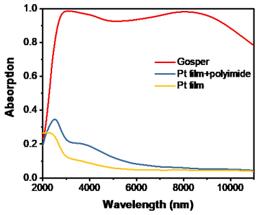
The central object is the Peano–Gosper space-filling curve rendered as a finite-width metallic trace: a fractal that packs many straight segments of different lengths, widths, and orientations into one unit cell. Each segment class acts as a small plasmonic antenna, so different wavelengths resonate in different parts of the curve, and the curve's space-filling property creates a dissipative plasmonic crystal in which adjacent segments couple. The absorber is completed by a platinum ground plane and a dielectric spacer that form a resonant cavity, plus a top dielectric layer that matches impedance to free space; the paper stresses that platinum's strong damping, not the fractal geometry alone, is what turns discrete resonances into one continuous broad absorption band.
What would settle it
Fabricate the four-layer stack described in the experimental-feasibility section and measure normal-incidence reflectance from 2.5 to 10 μm; if the spectrum does not show a 90% absorption band spanning at least most of 2.64–9.79 μm, or if the average absorption falls well below 95.78%, the central claim fails.
Extended reading notes
Core claim
The paper's central claim is that a single lithographically patterned layer of platinum, drawn as the third-stage Gosper curve, can act as a nearly perfect broadband mid-infrared absorber: average absorptivity 95.78% from 2.64 to 9.79 μm, a 90%-absorption bandwidth of 7.15 μm, with average absorption from 3 to 8 μm maintained above 90% under polarization changes and retaining 84% average absorption at 60° incidence. The authors attribute the band to multiple electric-dipole resonances localized on different segments of the Gosper curve, each excited at a different wavelength, combined with strong damping in platinum that prevents the deep spectral dips that would otherwise separate the resonances. This is presented as the broadest 90% bandwidth among single-layer mid-infrared metamaterial absorbers.
Load-bearing premise
The predicted 95.78% average absorption depends on the modeled platinum permittivity and an ideal lossless dielectric in a perfectly periodic, unfabricated structure; if real evaporated platinum or the dielectric's mid-infrared loss differs, the bandwidth and average absorption will change.
Editorial extensions
If this is right
- A fabricated version of this single-layer design would cover the full mid-infrared window with absorption above 90%, so thermal imagers and infrared detectors could work without multilayer stacks or multiple resonator sizes.
- The same Gosper geometry with different dielectric thicknesses, periods, and segment dimensions should shift or scale the absorption band, making the approach tunable to other infrared ranges.
- Because the absorber is polarization-insensitive up to 60° incidence, it could be placed on curved or moving surfaces without active realignment for applications that track a moving source.
- The claim that only electric resonances are involved distinguishes this design from conventional cut-wire or split-ring absorbers, pointing toward simpler design rules for future fractal absorbers.
Reading between the lines
- If experimentally confirmed, the absorber's near-blackbody mid-infrared response also makes it a candidate broadband thermal emitter: by the reciprocity of thermal radiation, heating it should produce a similar emission spectrum, which could be tested in a simple thermal-emission measurement.
- The design's reliance on platinum's intrinsic loss suggests a broader principle: replacing noble metals with refractory, lossy metals may be a general route to continuous broadband absorption in fractal plasmonic structures, not only for Gosper curves.
- A direct test would be to fabricate a few stage-3 Gosper cells with varied segment width and length and measure whether the resonance wavelengths scale as predicted by simple antenna length rules; this would isolate the role of the fractal geometry from the role of material damping.
- The simulations use an ideal lossless dielectric with refractive index 1.5; real spacer materials that absorb in the mid-infrared could degrade the claimed bandwidth, so a systematic dielectric-loss sweep would set fabrication tolerances.
Signed reviews
Editorial analysis
A structured set of objections, weighed in public.
Referee Report
Summary. This paper proposes a broadband mid-infrared (MIR) metamaterial perfect absorber based on the fractal Gosper curve. The structure comprises a Pt ground plane, a dielectric spacer (n=1.5), a Pt Gosper-curve resonator, and a top dielectric layer. Using FDTD (Lumerical) and FEM (COMSOL) simulations, the authors report an average absorptivity of 95.78% from 2.64 to 9.79 μm, a 90% absorption bandwidth of 7.15 μm, and claim insensitivity to polarization and incident angle. The physical mechanism is attributed to multiple electric resonances supported by different segments of the Gosper curve, which merge to form a continuous broadband absorption spectrum. The paper includes a cross-solver validation of the spectra, field and charge distributions at resonant wavelengths, parameter sweeps over geometry, and a comparison table with previously reported MIR absorbers.
Significance. If the reported performance holds, the Gosper-curve absorber would offer one of the broadest 90% absorption bandwidths among single-layer MIR metamaterial absorbers, and the use of a strongly damped metal (Pt) to merge resonances is a useful design idea. The paper provides a commendable cross-check between two independent solvers (FDTD and COMSOL, Appendix B, Fig. 8), which strengthens confidence in the numerical solution of Maxwell's equations for the specified geometry. The field-distribution analysis is also a positive feature: it gives qualitative support to the multi-resonance mechanism. However, the central quantitative claims (95.78% average absorption, 7.15 μm bandwidth) are simulation-only and rest on unvalidated constitutive models for Pt and on a lossless, non-dispersive dielectric. The paper does not provide sensitivity analysis for these material parameters, so the reported numbers are conditional on assumptions that are not tested.
major comments (3)
- [Section 4 and Appendix B] The manuscript explicitly states in Section 4 that 'this paper is limited to simulation work', and Appendix B specifies that Pt is modeled with fitted optical data from [49] while the dielectric is assigned a constant index n=1.5. No sensitivity analysis is provided for these constitutive parameters. The central claim of 95.78% average absorption and a 7.15 μm 90% bandwidth depends on overlapping resonances whose spectral positions and strengths are controlled by the Pt permittivity and the dielectric index and loss. Real Pt films differ from bulk fitted data (due to density, grain structure, and oxidation), and realistic MIR dielectrics have absorption bands in the 2.64–9.79 μm range; either effect could shift resonances below 90% and shrink the reported bandwidth. The FDTD/COMSOL agreement in Fig. 8 validates the numerical solver but not the physical inputs. I request a robustness study: repeat the simulation with alternative published Pt optical constants and with a dispersive, lossy dielectric model, and report how the 90% bandwidth and average absorption change.
- [Section 3.3 and Fig. 6] The abstract claims the absorber shows 'insensitivity to the polarization angle and the incident angle', but the simulation results in Fig. 6 and the text of Section 3.3 show a more limited behavior. The average absorption from 3 to 8 μm drops to 84% at 60° incidence for TM polarization, and the authors note that as the polarization angle changes, 'the average absorption and bandwidth decrease'. Calling this 'insensitive' overstates the robustness. The claim should be qualified to specify the ranges over which the absorption remains above 90% (e.g., up to 40° incidence for both TE and TM, and for polarization changes within a limited range), or the abstract should be revised to avoid an unqualified robustness statement.
- [Table 1] Table 1 compares the Gosper absorber with previously reported MIR absorbers but does not distinguish between experimental measurements and simulation-only results. Since the present work is simulation-only, comparing its simulated 95.8% average absorption and 7.15 μm bandwidth against references that may include measured devices is not an apples-to-apples comparison. The table should state explicitly, for each cited work, whether the quoted performance is experimental or simulated, and the benchmark claim ('highest bandwidth among single-layer counterparts') should be made contingent on that distinction.
minor comments (5)
- [Section 3.1] In the paragraph describing stage selection, the text says the stage 3 design 'provides a broad bandwidth in the NIR', but the operating range is the mid-infrared; this should be corrected to MIR.
- [Section 3.2] The sentence 'as the thickness increases and it induces a weaker coupling' is grammatically garbled and should be rewritten for clarity.
- [Appendix B] Appendix B begins 'For FET simulation', which appears to be a typo for 'FEM simulation'; please correct.
- [Fig. 10 caption] The caption lists wavelengths as '2500, 3085, 3085, 5136, 8055, and 10000 nm', with 3085 repeated; the duplicate should be removed.
- [Section 3.3] The phrase 'The angular sensitivity of the absorption for both TE and TM wave can be attributed to sensitivity of surface plasmon [48]' is awkward and would benefit from rewording, e.g., 'can be attributed to the angular sensitivity of surface plasmon excitations'.
Circularity Check
No significant circularity: the absorption spectrum is computed from Maxwell solvers for a specified geometry, and the headline figure is explicitly presented as an optimized simulation result, not as a prediction derived from its own inputs.
full rationale
The paper's central claim, an average absorptivity of 95.78% from 2.64 to 9.79 μm, is obtained by FDTD and FEM simulations of a fully specified Gosper-curve geometry with stated thicknesses, period, and material parameters (Section 3.1 and Appendix B). The spectrum is not defined in terms of the claimed bandwidth or average absorptivity; it is solved from Maxwell's equations and then post-processed into A(λ) = 1 − R(λ). The geometric parameters (td, t2, p, w, r) are varied in Section 3.2 and the reported result is explicitly called 'the optimized result,' so there is no fitted parameter disguised as an independent prediction. The mechanism discussion attributing broadband absorption to multiple electric resonances is an interpretation of field and loss distributions (Figs. 3–4, Appendix E), not a self-referential derivation. Self-citations appear (e.g., refs. [5], [19], [23], [40]) but they support background statements about metamaterial absorbers and fractal plasmonics; none is load-bearing for the computed spectrum or for the claimed bandwidth. The simulation-only limitation stated in Section 4 and the reliance on fitted Pt optical data from ref. [49] with n = 1.5 dielectric (Appendix B) are legitimate concerns about experimental robustness and material-model sensitivity, but they are correctness risks, not circularity. No equation, fitted parameter, or self-citation chain reduces the claimed performance to its own inputs, so the appropriate finding is no significant circularity.
Assumptions & free parameters
free parameters (5)
- Dielectric thickness td (t1 + t2 + t3) =
1250 nm (t1=595, t2=60, t3=595)
- Unit cell period p =
1550 nm
- Gosper segment length w =
80 nm
- Gosper segment width r =
40 nm
- Gosper layer thickness t2 =
60 nm
assumptions (5)
- standard math Maxwell's equations and the FDTD/FEM discretizations accurately model the plasmonic response at mid-infrared wavelengths.
- domain assumption Platinum optical constants from Rakic et al. [49] represent the deposited Pt films.
- domain assumption The dielectric spacer and cap can be modeled as lossless with n=1.5.
- domain assumption The 150 nm Pt ground plane is thick enough to block transmission, so absorption equals 1 minus reflection.
- domain assumption Periodic boundary conditions on one Gosper unit cell capture the response of an infinite periodic array.
Cite this review
Pith. "Pith review of Broadband mid-infrared perfect absorber using fractal Gosper curve." pith.science (2026). https://pith.science/paper/UPVUJ72P
@misc{pith2026190806635,
  author       = {Pith},
  title        = {Pith review of: Broadband mid-infrared perfect absorber using fractal Gosper curve},
  year         = {2026},
  howpublished = {\url{https://pith.science/paper/UPVUJ72P}},
  note         = {Machine review of arXiv:1908.06635}
}
read the original abstract
Designing broadband metamaterial perfect absorbers is challenging due to the intrinsically narrow bandwidth of surface plasmon resonances. Here, the paper reports an ultra-broadband metamaterial absorber by using space filling Gosper curve. The optimized result shows an average absorptivity of 95.78% from 2.64 to 9.79 {\mu}m across the entire mid-infrared region. Meanwhile, the absorber shows insensitivity to the polarization angle and the incident angle of the incident light. The underlying physical principles, used in our broadband absorber, involve a fractal geometry with multiple scales and a dissipative plasmonic crystal. The broadband perfect absorption can be attributed to multiple electric resonances at different wavelengths supported by a few segments in the defined Gosper curve.
Figures


Figures from the paper (1 more)

Reference graph
Works this paper leans on
-
[1]
Metamaterials and negative refractive index,
[1]. D. R. Smith, J. B. Pendry, and M. C. Wiltshire, "Metamaterials and negative refractive index," Science 305(5685), 788-792 (2004). [2]. V . M. Shalaev, "Optical negative-index metamaterials," Nat. Photonics 1(1), 41-48 (2007). [3]. N. I. Landy, S. Sajuyigbe, J. J. Mock, D. R. Smith, and W. J. Padilla, "Perfect metamaterial absorber," Phys. Rev. Lett. ...
work page 2004
-
[2]
Broadband Metamaterial Absorbers,
Wiederrecht, A. O. Govorov, and Z. Wang, "Broadband Metamaterial Absorbers," Adv. Opt. Mater. 7(3), 1800995 (2019). [6]. M. Diem, T. Koschny, and C. M. Soukoulis, "Wide -angle perfect 2500 nm 3085 nm 5136 nm 8055 nm 10000 nm H max H min absorber/thermal emitter in the terahertz regime," Phys. Rev. B 79(3), (2009). [7]. N. I. Landy, C. M. Bingham, T. Tyler...
work page 2019
-
[3]
A Switchable Mid -Infrared Plasmonic Perfect Absorber with Multispectral Thermal Imaging Capability,
Wuttig, T. Taubner, F. Neubrech, and H. Giessen, "A Switchable Mid -Infrared Plasmonic Perfect Absorber with Multispectral Thermal Imaging Capability," Adv. Mater. 27(31), 4597-4603 (2015). [10]. X. Liu, T. Tyler, T. Starr, A. F. Starr, N. M. Jokerst, and W. J. Padilla, "Taming the Blackbody with Infrared Metamaterials as Selective Thermal Emitters," Phys...
work page 2015
-
[4]
Omnidirectional absorption in nanostructured metal surfaces,
Bartlett, Y . Sugawara, and J. J. Baumberg, "Omnidirectional absorption in nanostructured metal surfaces," Nat. Photonics 2(5), 299-301 (2008). [12]. Y . Wang, T. Sun, T. Paudel, Y . Zhang, Z. Ren, and K. Kempa, "Metamaterial-plasmonic absorber structure f or high efficiency amorphous silicon solar cells," Nano Lett. 12(1), 440-445 (2012). [13]. P. Yu, F....
work page 2008
-
[5]
Design of a Perfect Black Absorber at Visible Frequencies Using Pl asmonic Metamaterials,
Tavassolizadeh, V . S. K. Chakravadhanula, V . Zaporojtchenko, T. Strunkus, F. Faupel, and M. Elbahri, "Design of a Perfect Black Absorber at Visible Frequencies Using Pl asmonic Metamaterials," Adv. Mater. 23(45), 5410 -5414 (2011). [35]. G. M. Akselrod, J. Huang, T. B. Hoang, P. T. Bowen, L. Su, D. R. Smith, and M. H. Mikkelsen, "Large -Area Metasurface...
work page 2011
Reviewed August 14, 2026 · model on record in the stance chip above.
Discussion (0). Continue with ORCID to comment.