REVIEW 5 minor 71 references
Breaking Bandwidth Limit: A Review of Broadband Doherty Power Amplifier Design for 5G
T0 review · 0 major / 5 minor · reviewed 2026-08-14 · deepseek-v4-flash
Pith's one-line read The Doherty amplifier's bandwidth bottleneck is a single quarter-wave transmission line, the impedance inverter TL1.
desk verdict A useful, well-organized review of broadband Doherty PA techniques; the tutorial math is standard but clean, and the survey is the real value. read the letter →
The pith
A machine-rendered reading of the paper's core claim, the machinery that carries it, and where it could break.
The reading
What carries the argument
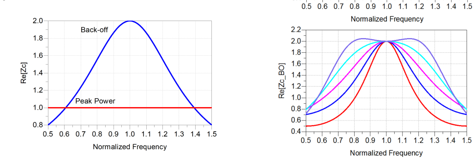
The central object is the quarter-wavelength transmission-line impedance inverter TL1 with characteristic impedance Z1 = Ropt. The paper models the impedance presented to the carrier amplifier by Zc(f) = Ropt (k + j tan(pi/2 * f/f0)) / (1 + j k tan(pi/2 * f/f0)), where k = 1 at peak power and k = 0.5 at 6-dB back-off, and uses the real part's frequency roll-off as the bandwidth metric. The mechanism doing the argumentative work is the impedance transformation ratio: TL1 acts as a 1:1 transformer at peak power and a 4:1 transformer at back-off, and a transmission-line transformer's bandwidth shrinks as its ratio grows. The derivation also introduces the parameter m = sqrt(Ropt / (2*RL)) to quantify how TL2's transformation ratio (2*RL/Ropt) further constrains bandwidth, and uses fractional bandwidth at 20% real-impedance reduction as the quantitative comparison baseline across designs.
What would settle it
Build or simulate a symmetric 6-dB Doherty PA with the stated Z1 = Ropt and Z2 = sqrt(RL*Ropt/2), bias the peaking device in class-C, and measure the real part of the impedance presented to the carrier device at back-off across frequency. If the frequency at which this impedance falls by 20% implies a fractional bandwidth substantially different from 38%, or if the back-off bandwidth proves to be set by TL2 or the peaking output impedance rather than TL1, the paper's central quantitative claim would be refuted.
Extended reading notes
Core claim
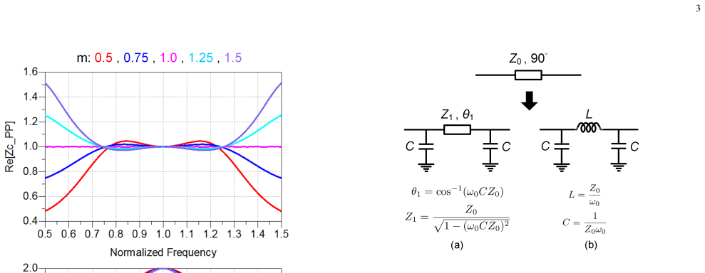
The central claim is that in a symmetric Doherty power amplifier, the back-off bandwidth is set by the impedance inverter TL1, not by the output matching line TL2 in the usual design. With characteristic impedances Z1 = Ropt and Z2 = sqrt(RL*Ropt/2), TL1 transforms its load by a ratio of 1 at peak power and 4 at 6-dB back-off, which the paper identifies as the main bandwidth constraint. The derived normalized impedance Zc(f) = Ropt (k + j tan(pi/2 * f/f0)) / (1 + j k tan(pi/2 * f/f0)), with k = 1 at peak power and k = 0.5 at 6-dB back-off, shows that the real part of the carrier impedance at back-off falls by 20% over a fractional bandwidth of about 38% for m = 1, while the peak-power impedance stays much flatter. Replacing TL2 with a two-section transformer restores 38% bandwidth for all values of m, and choosing m > 1 (for example with GaN devices having large Ropt) can widen back-off bandwidth to 62% at m = 1.5, at the cost of extra peaks in the peak-power impedance. The paper also claims that a higher-order matching network cannot simply replace TL1 because an impedance inverter must keep its inverse relationship between input and load impedance.
Load-bearing premise
The load-bearing premise is that at 6-dB back-off the peaking amplifier behaves as a perfect open circuit and at peak power as an ideal current source, and that all transmission lines are lossless; if the peaking transistor's real output impedance at back-off is not negligible, the derived impedances and the 38% bandwidth limit will not hold quantitatively.
Editorial extensions
If this is right
- If back-off bandwidth is governed by TL1's 1-to-4 transformation ratio, then broadband DPA designs should focus on reducing that ratio or compensating its frequency dependence, not on widening TL2.
- The m-parameter analysis implies that transistors with larger optimum load resistance, such as GaN devices, can push back-off bandwidth from 38% toward 62%, while small-Ropt CMOS devices will inherently have narrower load-modulation bandwidth.
- Replacing TL2 with a multi-section transformer can recover the ideal 38% back-off bandwidth for arbitrary m, but the impedance inverter TL1 cannot be similarly replaced by a higher-order matching network.
- Parasitic-absorption techniques, such as reduced-length or lumped-element transmission lines, absorb the drain-source capacitance only at one frequency and degrade bandwidth, so true wideband IC DPAs must use other compensation, post-matching, or dual-input strategies.
- Among the reviewed techniques, dual-input digital control achieves octave bandwidth (1-3 GHz, 100%) in a reported GaN design, indicating that frequency-dependent input drive can compensate what the output network cannot.
Reading between the lines
- My inference: if the peaking amplifier's finite output conductance at back-off were included in Eq. (3), the 38% figure would likely shrink or shift, making the review's quantitative limits optimistic for real transistors; a direct re-derivation with a shunt conductance would test this.
- My inference: the same ratio-based reasoning could be applied to asymmetric DPAs, where the paper notes the transformation ratio grows to (N+1)*RL/Ropt for an N-times peaking device, so the bandwidth penalty of higher-PAPR operation is likely even steeper than the symmetric 6-dB case suggests.
- My inference: the surveyed techniques are mostly demonstrated in discrete GaN at sub-4 GHz; extending them to mm-wave ICs may require lumped-element equivalents of TL1, and the paper's claim that lumped-element inverters are narrowband suggests a fundamental trade-off that future work must break, for instance by nonreciprocal or active load modulation.
- My inference: a testable prediction follows from the paper: DPA designs with m = 1 should cluster near the 38% back-off bandwidth bound unless they employ one of the surveyed compensation techniques, so a meta-analysis of reported designs could check whether the derivation explains observed bandwidths.
Signed reviews
Editorial analysis
A structured set of objections, weighed in public.
Referee Report
Summary. The manuscript is a review and tutorial on bandwidth-extension techniques for Doherty power amplifiers (DPAs) targeting 5G applications. Section II derives the main bandwidth limitation of the classical DPA from the impedance presented to the carrier amplifier, identifying the impedance inverter TL1 as the principal back-off bandwidth limiter and quantifying a 38% fractional bandwidth for a 20% reduction in the real part of the back-off impedance. Section III surveys modified load-modulation networks, frequency-response optimization, parasitic compensation, post-matching DPAs, distributed DPAs, dual-input DPAs, and transformer-based/transformer-less load-modulated PAs, with a comparative performance table. Section IV discusses integrated-circuit implementation challenges and reviews RF and mm-wave IC DPAs, and Section V offers conclusions about the most promising techniques for IC integration.
Significance. If the claims hold, the paper provides a useful structured map of the broadband-DPA field and a compact quantitative account of why the DPA back-off bandwidth is dominated by the impedance inverter TL1. The tutorial derivations are standard and internally consistent, the survey table is informative, and the critical discussion of each technique's drawbacks is a valuable feature. The treatment of IC and mm-wave implementations is a strength, and the authors are careful to flag assumptions (ideal peaking open/current source, lossless transmission lines) and to point out where published bandwidths come with efficiency ripple. No original measurements are presented, but none are required for a review of this type.
minor comments (5)
- [Section II-A, after Eq. (5)] The sentence stating that the impedance transformation ratio of TL1 at back-off is (N+1)RL/Ropt is inconsistent with the impedances defined just above it: TL1 transforms Ropt/(N+1) to (N+1)Ropt, so its back-off ratio is (N+1)^2 (equal to 4 for N=1), whereas (N+1)RL/Ropt is the ratio for TL2. Please correct the formula and the surrounding wording.
- [Table I caption] The symbols ηPP and ηBO are used in the table but are not defined in the caption; please define them as drain efficiency at peak power and at back-off, and state that the bandwidth values are fractional bandwidths.
- [References [13] and [39]] The reference formatting is malformed in two places: [13] gives page numbers '505507' instead of '505–507', and [39] contains a duplicated/confused citation string ('pp. 1–14, 2017. vol. 64, no. 7, pp. 1758–1771'); please correct both entries.
- [Section II-B] For the lumped-element equivalent circuit in Fig. 5(b), the bound is given as Cds < C = 1/(Z0ω0); please explicitly identify Z0 and ω0 in the text or figure caption so that the condition is self-contained.
- [Section III-A2, discussion of [18]] The sentence 'the impedance transformation ratio is 2 in both cases' would be clearer if the two load impedances (100 Ω and 50 Ω) were named explicitly, since the definition of transformation ratio is not repeated in that paragraph.
Circularity Check
No significant circularity: the tutorial derivation is self-contained standard transmission-line analysis and the review's claims rest on external literature.
full rationale
The paper's central quantitative content, Section II-A, derives the carrier impedance Zc(f) from the classical quarter-wave transmission-line equation with Z1 = Ropt, Z2 = sqrt(RL Ropt / 2), k = 1 at peak power and k = 0.5 at back-off. The resulting Eqs. (3)-(4) and the stated 38% fractional bandwidth are computed from these standard assumptions, not fitted to data and not imported from the authors' own prior results. The review's organizing taxonomy is supported by external literature measurements tabulated in Table I; the self-citations ([45], [55], [56], and [37]) appear only as background references or as one entry in the survey and do not supply the derivation's premises. The idealizations used in the derivation, such as an open-circuit peaking amplifier at back-off and lossless transmission lines, are explicitly stated and subsequently relaxed in Sections II-B and III-C, so the simplification is disclosed rather than hidden. No prediction in the paper is equivalent by construction to an input, and no fitted parameter is renamed as a derived result. The paper is a review with a tutorial, and its claims are traceable to standard theory and external experimental reports; therefore no meaningful circularity is present.
Assumptions & free parameters
assumptions (3)
- standard math Lossless uniform transmission line equations (telegrapher's equations) for the quarter-wave lines TL1 and TL2
- domain assumption Ideal Doherty operation: peaking amplifier is an open circuit at back-off and an ideal current source at peak power; carrier and peaking transistors have identical optimum load Ropt in the symmetric case
- standard math Quarter-wave transmission line at center frequency f0 provides exact 90-degree phase shift and impedance inversion
Cite this review
Pith. "Pith review of Breaking Bandwidth Limit: A Review of Broadband Doherty Power Amplifier Design for 5G." pith.science (2026). https://pith.science/paper/Y6TCLT6V
@misc{pith2026190807755,
  author       = {Pith},
  title        = {Pith review of: Breaking Bandwidth Limit: A Review of Broadband Doherty Power Amplifier Design for 5G},
  year         = {2026},
  howpublished = {\url{https://pith.science/paper/Y6TCLT6V}},
  note         = {Machine review of arXiv:1908.07755}
}
read the original abstract
The Doherty power amplifier (DPA) has been extensively explored in the past and has become one of the most widely used power amplifier (PA) architectures in cellular base stations. The classical DPA suffers intrinsic bandwidth constrains which limit its application in future 5G wireless transmitters. In this paper, we present a comprehensive review of the DPA bandwidth enhancement techniques proposed in literature in order to provide a thorough understanding of the DPA's broadband design for high-efficiency 5G wireless transmitters. We elaborate on the main bandwidth limitation sources and provide circuit design insights. We then follow with an overview of bandwidth enhancement techniques developed for the DPA, including modified load-modulation networks, frequency response optimization, parasitic compensation, post-matching, as well as distributed DPA, dual-input digital DPA, transformer-based power-combining PA, and transformer-less load modulated PA architectures. Furthermore, challenges and design techniques for integrated circuit (IC) implementation of broadband DPAs are discussed, including a review of circuits developed in CMOS, SiGe, and GaN processes, and operating in RF and mm-Wave frequencies.
Figures

Figures from the paper (23 more)




Reference graph
Works this paper leans on
-
[45]
The (r)evolution of distributed amplifiers: From vacuum tubes to modern CMOS and GaN ICs,
G. Nikandish, R. B. Staszewski, and A. Zhu, “The (r)evolution of distributed amplifiers: From vacuum tubes to modern CMOS and GaN ICs,” IEEE Microw. Mag., vol. 19, no. 4, pp. 66–83, Jun. 2018
work page 2018
-
[55]
G. Nikandish and A. Medi, “A design procedure for high-efficiency and compact-size 5–10-W MMIC power amplifiers in GaAs pHEMT technology,” IEEE Trans. Microw. Theory Techn. , vol. 61, no. 8, pp. 2922–2933, Aug. 2013
work page 2013
-
[56]
G. Nikandish, E. Babakrpur, and A. Medi, “A harmonic termination technique for single- and multi-band high-efficiency class-F MMIC power amplifiers,” IEEE Trans. Microw. Theory Techn. , vol. 62, no. 5, pp. 1212–1220, May 2014
work page 2014
-
[1]
Millimeter wave mobile communications for 5G cellular: It will work!,
T. S. Rappaport et al., “Millimeter wave mobile communications for 5G cellular: It will work!,” IEEE Access, vol. 1, pp. 335–349, May 2013
work page 2013
- [2]
-
[3]
Design of energy- and cost-efficient massive MIMO arrays,
A. Puglielli et al., “Design of energy- and cost-efficient massive MIMO arrays,” Proc. IEEE, vol. 104, no. 3, pp. 586–606, Mar. 2016
work page 2016
-
[4]
A new high efficiency power amplifier for modulated waves,
W. H. Doherty, “A new high efficiency power amplifier for modulated waves,”Proc. Inst. Radio Eng., vol. 24, no. 9, pp. 1163–1182, Sep. 1936
work page 1936
-
[5]
Will Doherty continue to rule for 5G?,
P. M. Asbeck, “Will Doherty continue to rule for 5G?,” in Proc. IEEE MTT-S Int. Microwave Symp. Dig. , May 2016, pp. 1–4
work page 2016
Show all 71 references
-
[6]
High-efficiency Doherty power amplifiers: Historical aspect and modern trends,
B. A. Grebennikov and S. Bulja, “High-efficiency Doherty power amplifiers: Historical aspect and modern trends,” Proc. IEEE, vol. 100, no. 12, pp. 3190–3219, 2012
2012
-
[7]
The Doherty power amplifier,
B. Kim, K. Jangheon, K. Ildu, and C. Jeonghyeon, “The Doherty power amplifier,” IEEE Microw. Mag., vol. 7, no. 5, pp. 42–50, 2006
2006
-
[8]
Advanced Doherty architecture,
B. Kim, I. Kim, and J. Moon, “Advanced Doherty architecture,” IEEE Microw. Mag., vol. 11, no. 5, pp. 72–86, Aug. 2010
2010
-
[9]
The Doherty power amplifier: Review of recent solutions and trends,
V . Camarchia, M. Pirola, R. Quaglia, S. Jee, Y . Cho, and B. Kim, “The Doherty power amplifier: Review of recent solutions and trends,” IEEE Trans. Microw. Theory Techn., vol. 63, no. 2, pp. 559–571, 2015
2015
-
[10]
Doherty goes digital: Digitally enhanced Doherty power amplifiers,
R. Darraji, P. Mousavi, and F. M. Ghannouchi, “Doherty goes digital: Digitally enhanced Doherty power amplifiers,” IEEE Microw. Mag., vol. 17, no. 8, pp. 41–51, Aug. 2016
2016
-
[11]
Doherty’s legacy: A history of the Doherty power amplifier from 1936 to the present day,
R. Pengelly, C. Fager, and M. Ozen, “Doherty’s legacy: A history of the Doherty power amplifier from 1936 to the present day,” IEEE Microw. Mag., vol. 17, no. 2, pp. 41–58, Feb. 2016
1936
-
[12]
AM/AM and AM/PM distortion generation mechanisms in Si LDMOS and GaN HEMT based RF power amplifiers,
L. C. Nunes, P. M. Cabral, and J. C. Pedro, “AM/AM and AM/PM distortion generation mechanisms in Si LDMOS and GaN HEMT based RF power amplifiers,” IEEE Trans. Microw. Theory Techn., vol. 62, no. 4, pp. 799–809, Apr. 2014
2014
-
[13]
Effect of load modulation on phase distortion in Doherty power amplifiers,
L. Piazzon et al. , “Effect of load modulation on phase distortion in Doherty power amplifiers,” IEEE Microw. Wireless Compon. Lett. , vol. 24, no. 7, pp. 505507, Jul. 2014
2014
-
[14]
Frequency response analysis and bandwidth extension of the Doherty amplifier,
K. Bathich, A. Z. Markos, and G. Boeck, “Frequency response analysis and bandwidth extension of the Doherty amplifier,” IEEE Trans. Microw. Theory Techn., vol. 59, no. 4, pp. 934–944, Apr. 2011
2011
-
[15]
A modified Doherty configuration for broadband amplification using symmetrical devices,
D. Y .-T. Wu and S. Boumaiza, “A modified Doherty configuration for broadband amplification using symmetrical devices,” IEEE Trans. Microw. Theory Techn., vol. 60, no. 10, pp. 3201–3213, Oct. 2012
2012
-
[16]
A modified Doherty power amplifier with extended bandwidth and reconfigurable efficiency,
D. Gustafsson, C. M. Andersson, and C. Fager, “A modified Doherty power amplifier with extended bandwidth and reconfigurable efficiency,” IEEE Trans. Microw. Theory Techn. , vol. 60, no. 1, pp. 533–542, Jan. 2013
2013
-
[17]
Generalized theory and design methodology of wideband Doherty amplifiers applied to the realization of an octave-bandwidth prototype,
R. Darraji, D. Bhaskar, T. Sharma, M. Helaoui, P. Mousavi, and F. M. Ghannouchi, “Generalized theory and design methodology of wideband Doherty amplifiers applied to the realization of an octave-bandwidth prototype,”IEEE Trans. Microw. Theory Techn., vol. 65, no. 8, pp. 3014– 3...
2017
-
[18]
A dual-band parallel Doherty power amplifier for wireless applications,
A. Grebennikov and J. Wong, “A dual-band parallel Doherty power amplifier for wireless applications,” IEEE Trans. Microw. Theory Techn., vol. 60, no. 10, pp. 3214–3222, Oct. 2012
2012
-
[19]
A 350 W, 790 to 960 MHz wideband LDMOS Doherty amplifier using a modified combining scheme,
D. Y .-T. Wu, J. Annes, M. Bokatius, P. Hart, E. Krvavac, and G. Tucker, “A 350 W, 790 to 960 MHz wideband LDMOS Doherty amplifier using a modified combining scheme,” in IEEE MTT-S Int. Microw. Symp. Dig., Jun. 2014, pp. 1–4
2014
-
[20]
A closed-form design technique for ultra-wideband Doherty power amplifiers,
R. Giofre, L. Piazzon, P. Colantonio, and F. Giannini, “A closed-form design technique for ultra-wideband Doherty power amplifiers,” IEEE Trans. Microw. Theory Techn. , vol. 62, no. 12, pp. 3414–3424, Dec. 2014
2014
-
[21]
A distributed matching/combining network suitable for Doherty power amplifiers covering more than an octave frequency band,
R. Giofre, L. Piazzon, P. Colantonio, and F. Giannini, “A distributed matching/combining network suitable for Doherty power amplifiers covering more than an octave frequency band,” inMicrowave Symposium (IMS), 2014 IEEE MTT-S International , 2014, pp. 1–3
2014
-
[22]
An ultra- broadband GaN Doherty amplifier with 83% of fractional bandwidth,
R. Giofre, L. Piazzon, P. Colantonio, and F. Giannini, “An ultra- broadband GaN Doherty amplifier with 83% of fractional bandwidth,” IEEE Microw. Wireless Compon. Lett. , vol. 24, no. 11, pp. 775–777, Nov. 2014
2014
-
[23]
Toward a more generalized Doherty power amplifier design for broadband operation,
A. Barakat, M. Thian, V . Fusco, S. Bulja, and L. Guan, “Toward a more generalized Doherty power amplifier design for broadband operation,” IEEE Trans. Microw. Theory Techn. , vol. 65, no. 3, pp. 846–859, Mar. 2017
2017
-
[24]
A wideband 700W push-pull Doherty amplifier,
J. He, J. H. Qureshi, W. Sneijers, D. A. Calvillo-Cortes, and L. C. N. de Vreede, “A wideband 700W push-pull Doherty amplifier,” IEEE MTT-S Int. Microwave Symp. , Phoneix, 2015
2015
-
[25]
A Doherty architecture with high feasibility and defined bandwidth behavior,
R. Giofre, L. Piazzon, P. Colantonio, and F. Giannini, “A Doherty architecture with high feasibility and defined bandwidth behavior,” IEEE Trans. Microw. Theory Techn., vol. 61, no. 9, pp. 3308–3317, Sep. 2013
2013
-
[26]
A wideband Doherty architecture with 36% of fractional bandwidth,
L. Piazzon, R. Giofre, P. Colantonio, and F. Giannini, “A wideband Doherty architecture with 36% of fractional bandwidth,” IEEE Microw. Wireless Compon. Lett., vol. 23, no. 11, pp. 626–628, Nov. 2013
2013
-
[27]
A bandwidth enhanced Do- herty power amplifier with a compact output combiner,
S. Chen, G. Wang, Z. Cheng, and Q. Xue, “A bandwidth enhanced Do- herty power amplifier with a compact output combiner,” IEEE Microw. Wireless Compon. Lett., vol. 26, no. 6, pp. 434–436, Jun. 2016
2016
-
[28]
A broadband three- device Doherty power amplifier based on a modified load modulation network,
S. Chen, P. Qiao, G. Wang, Z. Cheng, and Q. Xue, “A broadband three- device Doherty power amplifier based on a modified load modulation network,” in Microwave Symposium (IMS), 2016 IEEE MTT-S Interna- tional, 2016, pp. 1–4
2016
-
[29]
An extended bandwidth Doherty amplifier using a novel output combiner,
M. N. Ali Abadi, H. Golestaneh, H. Sarbishaei, and S. Boumaiza, “An extended bandwidth Doherty amplifier using a novel output combiner,” IEEE MTT-S Int. Microwave Symp. Dig. , 2014, pp. 1–4
2014
-
[30]
Broadband Doherty power amplifier via real frequency technique,
G. Sun and R. H. Jansen, “Broadband Doherty power amplifier via real frequency technique,” IEEE Trans. Microw. Theory Techn., vol. 60, no. 1, pp. 99–111, Jan. 2012
2012
-
[31]
Wideband harmonically-tuned GaN Doherty power amplifier,
K. Bathich and G. Boeck, “Wideband harmonically-tuned GaN Doherty power amplifier,” inProc. 2012 IEEE MTT-S Int. Microwave Symp. Dig., Jun. 2012, pp. 1–3
2012
-
[32]
Multiobjective Bayesian optimization for active load modulation in a broadband 20-W GaN Doherty power amplifier design,
P. Chen, J. Xia, B. M. Merrick, and T. J. Brazil, “Multiobjective Bayesian optimization for active load modulation in a broadband 20-W GaN Doherty power amplifier design,” IEEE Trans. Microw. Theory Techn. , vol. 65, no. 3, pp. 860–871, Mar. 2017
2017
-
[33]
A wideband 20 W LMOS Doherty power amplifier,
J. H. Qureshi, N. Li, W. C. E. Neo, F. Rijs, I. Blednov, and L. C. N. de Vreede, “A wideband 20 W LMOS Doherty power amplifier,” in IEEE MTT-S Int. Microw. Symp. Dig ., Anaheim, CA, May 2010, pp. 1504–1507
2010
-
[34]
3–3.6-GHz wideband GaN Doherty power amplifier exploiting output compensation stages,
J. Rubio, J. Fang, V . Camarchia, R. Quaglia, M. Pirola, and G. Ghione, “3–3.6-GHz wideband GaN Doherty power amplifier exploiting output compensation stages,” IEEE Trans. Microw. Theory Techn., vol. 60, no. 8, pp. 2543–2548, Aug. 2012
2012
-
[35]
Design of an 87% fractional bandwidth Doherty power amplifier supported by a simplified bandwidth estimation method,
J. J. M. Rubio, V . Camarchia, M. Pirola, and R. Quaglia, “Design of an 87% fractional bandwidth Doherty power amplifier supported by a simplified bandwidth estimation method,” IEEE Trans. Microw. Theory Techn., vol. 66, no. 3, pp. 1319–1327, Mar. 2018
2018
-
[36]
Frequency analysis and multiline implementation of compensated impedance in- verter for wideband Doherty high-power amplifier design,
A. Cidronali, S. Maddio, N. Giovannelli, and G. Collodi, “Frequency analysis and multiline implementation of compensated impedance in- verter for wideband Doherty high-power amplifier design,” IEEE Trans. Microw. Theory Techn., vol. 64, no. 5, pp. 1359–1372, May 2016
2016
-
[37]
A broadband high-efficiency Doherty power amplifier with integrated compensating reactance,
J. Xia, M. Yang, Y . Guo, and A. Zhu, “A broadband high-efficiency Doherty power amplifier with integrated compensating reactance,” IEEE Trans. Microw. Theory Techn., vol. 64, no. 7, pp. 2014–2024, Jul. 2016
2014
-
[38]
A post-matching Doherty power amplifier employing low-order impedance inverters for broadband applications,
J. Pang, S. He, C. Huang, Z. Dai, J. Peng, and F. You, “A post-matching Doherty power amplifier employing low-order impedance inverters for broadband applications,” IEEE Trans. Microw. Theory Techn. , vol. 63, no. 12, pp. 4061–4071, Dec. 2015
2015
-
[39]
Broadband efficiency-enhanced mutually coupled harmonic postmatching Doherty power amplifier,
X. Y . Zhou, S. Y . Zheng, W. S. Chan, S. Chen, and D. Ho, “Broadband efficiency-enhanced mutually coupled harmonic postmatching Doherty power amplifier,” IEEE Trans. Circuits Syst. I, Reg. Papers , pp. 1–14,
-
[40]
Octave bandwidth Doherty power amplifier using multiple resonance circuit for the peaking amplifier,
H. Kang et al. , “Octave bandwidth Doherty power amplifier using multiple resonance circuit for the peaking amplifier,” IEEE Trans. on Circuits and Systems I: Reg. Papers. DOI: 10.1109/TCSI.2018.2869905
2018
-
[41]
On the continuity of high efficiency modes in linear RF power amplifiers,
S. C. Cripps, P. J. Tasker, A. L. Clarke, J. Lees, and J. Benedikt, “On the continuity of high efficiency modes in linear RF power amplifiers,” IEEE Microw. Wireless Compon. Lett. , vol. 19, no. 10, pp. 665–667, Oct. 2009
2009
-
[42]
A broadband Doherty power amplifier based on continuous-mode technology,
X. Chen, W. Chen, F. M. Ghannouchi, Z. Feng, and Y . Liu, “A broadband Doherty power amplifier based on continuous-mode technology,” IEEE 15 Trans. Microw. Theory Techn. , vol. 64, no. 12, pp. 4505–4517, Dec. 2016
2016
-
[43]
A 200W broadband continuous-mode Doherty power amplifier for base- station applications,
X. Chen, W. Chen, Q. Zhang, F. M. Ghannouchi, and Z. Feng, “A 200W broadband continuous-mode Doherty power amplifier for base- station applications,” IEEE MTT-S Int. Microwave Symp. Dig., 2017, pp. 1110–1113
2017
-
[44]
Broadband continuous-mode Doherty power amplifiers with noninfinity peaking impedance,
W. Shi et al., “Broadband continuous-mode Doherty power amplifiers with noninfinity peaking impedance,” IEEE Trans. Microw. Theory Techn., vol. 66, no. 2, pp. 1034–1046, Feb. 2018
2018
-
[46]
A new wideband distributed Doherty amplifier for WCDMA repeater applications,
Y . Lee, M. Lee, S. Kam, and Y . Jeong, “A new wideband distributed Doherty amplifier for WCDMA repeater applications,” IEEE Microw. Wireless Compon. Lett., vol. 19, no. 10, pp. 668–670, Oct. 2009
2009
-
[47]
Adaptive input-power distribution in Doherty power amplifiers for linearity and efficiency enhancement,
M. Nick and A. Mortazawi, “Adaptive input-power distribution in Doherty power amplifiers for linearity and efficiency enhancement,” IEEE Trans. Microw. Theory Techn. , vol. 58, no. 11, pp. 2764–2771, Nov. 2010
2010
-
[48]
Mitigation of bandwidth limitation in wireless Doherty amplifiers with substantial bandwidth enhancement using digital techniques,
R. Darraji, F. M. Ghannouchi, and M. Helaoui, “Mitigation of bandwidth limitation in wireless Doherty amplifiers with substantial bandwidth enhancement using digital techniques,” IEEE Trans. Microw. Theory Techn., vol. 60, no. 9, pp. 2875–2885, Sept. 2012
2012
-
[49]
A 1–3-GHz digitally controlled dual-RF input power-amplifier design based on a Doherty-Outphasing continuum analysis,
C. M. Andersson, D. Gustafsson, J. Chani Cahuana, R. Hellberg, and C. Fager, “A 1–3-GHz digitally controlled dual-RF input power-amplifier design based on a Doherty-Outphasing continuum analysis,”IEEE Trans. Microw. Theory Techn., vol. 61, no. 10, pp. 3743–3752, Oct. 2013
2013
-
[50]
Digitally equalized Doherty RF front-end architecture for broadband and multi- standard wireless transmitters,
R. Darraji, A. K. Kwan, F. M. Ghannouchi, and M. Helaoui, “Digitally equalized Doherty RF front-end architecture for broadband and multi- standard wireless transmitters,” IEEE Trans. Microw. Theory Techn., vol. 63, no. 6, pp. 1978–1988, Jun. 2015
1978
-
[51]
Fully integrated CMOS power amplifier with efficiency enhancement at power back-off,
G. Liu, P. Haldi, T.-J. K. Liu, and A. M. Niknejad, “Fully integrated CMOS power amplifier with efficiency enhancement at power back-off,” IEEE J. Solid-State Circuits , vol. 43, no. 3, pp. 600–609, Mar. 2008
2008
-
[52]
Transformer-less load- modulated (TLLM) architecture for efficient wideband power ampli- fiers,
M. Akbarpour, M. Helaoui, and F. Ghanouchi, “Transformer-less load- modulated (TLLM) architecture for efficient wideband power ampli- fiers,” IEEE Trans. Microw. Theory Techn. , vol. 60, no. 9, pp. 2863– 2874, Sept. 2012
2012
-
[53]
Design of GaN Doherty power amplifiers for broadband applications,
J. Shao et al., “Design of GaN Doherty power amplifiers for broadband applications,” IEEE Microw. Wireless Compon. Lett., vol. 24, no. 4, pp. 248–250, Apr. 2014
2014
-
[54]
A miniature broadband Doherty power amplifier with a series-connected load,
S. Watanabe, Y . Takayama, R. Ishikawa, and K. Honjo, “A miniature broadband Doherty power amplifier with a series-connected load,” IEEE Trans. Microw. Theory Techn., vol. 63, no. 2, pp. 572–579, Feb. 2015
2015
-
[57]
Design of bandwidth-enhanced Doherty power amplifiers for handset applications,
D. Kang, D. Kim, Y . Cho, B. Park, J. Kim, and B. Kim, “Design of bandwidth-enhanced Doherty power amplifiers for handset applications,” IEEE Trans. Microw. Theory Techn. , vol. 59, no. 12, pp. 3474–3483, Dec. 2011
2011
-
[58]
Asymmetric broadband Doherty power amplifier using GaN MMIC for femto-cell base-station,
S. Jee et al. , “Asymmetric broadband Doherty power amplifier using GaN MMIC for femto-cell base-station,” IEEE Trans. Microw. Theory Techn., vol. 63, no. 9, pp. 2802–2810, Sep. 2015
2015
-
[59]
A wideband and compact GaN MMIC Doherty amplifier for microwave link applications,
D. Gustafsson, J. C. Cahuana, D. Kuylenstierna, I. Angelov, N. Rorsman, and C. Fager, “A wideband and compact GaN MMIC Doherty amplifier for microwave link applications,” IEEE Trans. Microw. Theory Techn. , vol. 61, no. 2, pp. 922–930, Feb. 2013
2013
-
[60]
A GaN MMIC modified Doherty PA with large bandwidth and reconfigurable efficiency,
D. Gustafsson, J. C. Cahuana, D. Kuylenstierna, I. Angelov, and C. Fager, “A GaN MMIC modified Doherty PA with large bandwidth and reconfigurable efficiency,” IEEE Trans. Microw. Theory Techn., vol. 62, no. 12, pp. 3006–3016, Dec. 2014
2014
-
[61]
A highly efficient and linear power amplifier for 28-GHz 5G phased array radios in 28-nm CMOS,
S. Shakib, H.-C. Park, J. Dunworth, V . Aparin, and K. Entesari, “A highly efficient and linear power amplifier for 28-GHz 5G phased array radios in 28-nm CMOS,” IEEE J. Solid-State Circuits , vol. 51, no. 12, pp. 3020–3036, Dec. 2016
2016
-
[62]
A wideband class-AB power amplifier with 29–57-GHz AM-PM compensation in 0.9-V 28-nm bulk CMOS,
M. Vigilante and P. Reynaert, “A wideband class-AB power amplifier with 29–57-GHz AM-PM compensation in 0.9-V 28-nm bulk CMOS,” IEEE J. Solid-State Circuits , vol. 53, no. 5, pp. 1288–1301, May 2018
2018
-
[63]
Active millimeter-wave phase-shift Doherty power amplifier in 45-nm SOI CMOS,
A. Agah, H. T. Dabag, B. Hanafi, P. M. Asbeck, J. F. Buckwalter and L. E. Larson, “Active millimeter-wave phase-shift Doherty power amplifier in 45-nm SOI CMOS,” IEEE J. Solid-State Circuits, vol. 48, no. 10, pp. 2338–2350, Oct. 2013
2013
-
[64]
Transformer-based Doherty power amplifiers for mm-Wave applications in 40-nm CMOS,
E. Kaymaksut, D. Zhao, and P. Reynaert, “Transformer-based Doherty power amplifiers for mm-Wave applications in 40-nm CMOS,” IEEE Trans. Microw. Theory Techn., vol. 63, no. 4, pp. 1186–1192, Apr. 2015
2015
-
[65]
A 28GHz/37GHz/39GHz multiband linear Doherty power amplifier for 5G massive MIMO applications,
S. Hu, F. Wang, and H. Wang, “A 28GHz/37GHz/39GHz multiband linear Doherty power amplifier for 5G massive MIMO applications,” in IEEE Int. Solid-State Circuits Conf. (ISSCC) Dig. Tech. Papers , Feb. 2017, pp. 32–33
2017
-
[66]
A 38–46 GHz MMIC Doherty power amplifier using post-distortion linearization,
J. H. Tsai and T. W. Huang, “A 38–46 GHz MMIC Doherty power amplifier using post-distortion linearization,” IEEE Microw. Wireless Compon. Lett., vol. 17, no. 5, pp. 388–390, May 2007
2007
-
[67]
Efficient millimeter wave Doherty PA design based on a low-loss combiner synthesis technique,
M. Ozen, N. Rostomyan, K. Aufinger, and C. Fager, “Efficient millimeter wave Doherty PA design based on a low-loss combiner synthesis technique,” IEEE Microw. Wireless Compon. Lett. , vol. 27, no. 12, pp. 1143–1145, Dec. 2017
2017
-
[68]
28 GHz Doherty power amplifier in CMOS SOI with 28% back-off PAE,
N. Rostomyan, M. Ozen and P. Asbeck, “28 GHz Doherty power amplifier in CMOS SOI with 28% back-off PAE,” IEEE Microw. Wireless Compon. Lett., vol. 28, no. 5, pp. 446–448, May 2018
2018
-
[69]
A 32 GHz 20 dBm-P SAT transformer- based Doherty power amplifier for multi-Gb/s 5G applications in 28 nm bulk CMOS,
P. Indirayanti and P. Reynaert, “A 32 GHz 20 dBm-P SAT transformer- based Doherty power amplifier for multi-Gb/s 5G applications in 28 nm bulk CMOS,” in IEEE RFIC Symp. Dig. Papers , Jun. 2017, pp. 45–48
2017
-
[70]
Simultaneously broadband and back-off efficient mm-wave PAs: A multi-port network synthesis approach,
C. R. Chappidi, X. Wu and K. Sengupta, “Simultaneously broadband and back-off efficient mm-wave PAs: A multi-port network synthesis approach,” IEEE J. Solid-State Circuits , vol. 53, no. 9, pp. 2543–2559, Sept. 2018
2018
-
[2017]
vol. 64, no. 7, pp. 1758–1771, Jul. 2017
2017
Reviewed August 14, 2026 · model on record in the stance chip above.
Discussion (0). Continue with ORCID to comment.