REVIEW 2 major objections 4 minor 42 references
Simple Thermal Noise Estimation of Switched Capacitor Circuits Based on OTAs -- Part I: Amplifiers with Capacitive Feedback
T0 review · 2 major / 4 minor · reviewed 2026-08-14 · deepseek-v4-flash
Pith's one-line read This paper claims that thermal noise in OTA-based switched-capacitor circuits can be estimated from three capacitances read off capacitor-only equivalent circuits, avoiding transfer functions and integrals.
desk verdict A genuinely useful design-oriented noise estimation method for OTA-based switched-capacitor circuits, sound under its stated assumptions, but the GmRon << 1 regime needs a quantitative bound and one real-OTA validation. read the letter →
The pith
A machine-rendered reading of the paper's core claim, the machinery that carries it, and where it could break.
The reading
What carries the argument
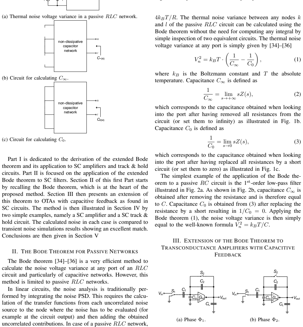
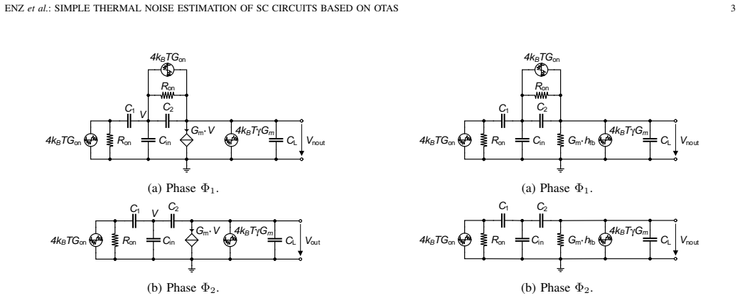
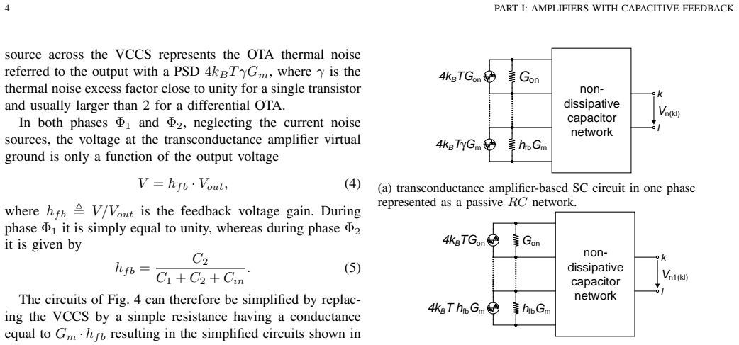
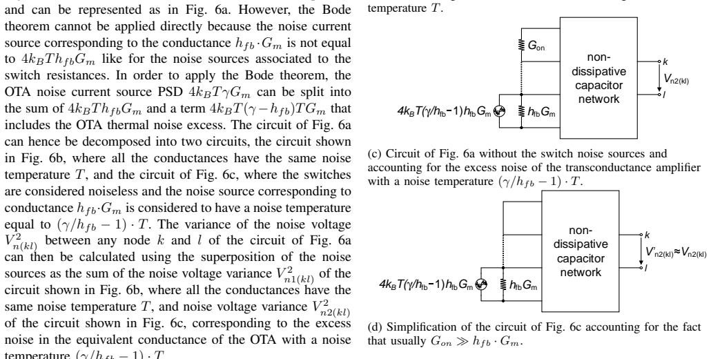
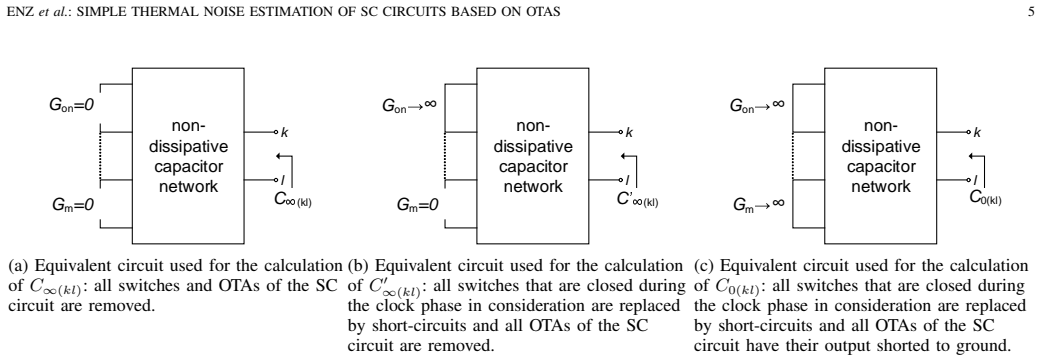
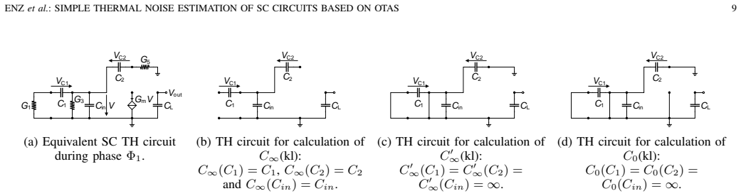
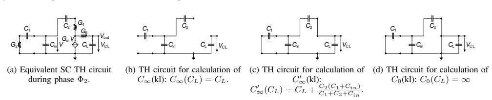
The load-bearing object is the extended Bode theorem expressed by Eq. (9), together with the three capacitor-only inspection circuits that define $C_\infty$, $C'_\infty$, and $C_0$. The mechanism is a decomposition of the OTA noise current source into a part at ambient temperature $T$ that joins the switch noises in a passive network, plus an excess-noise part at temperature $(\gamma/h_{fb}-1)T$ evaluated after the switches are shorted. This reduction converts a cyclostationary sampled-noise problem into three capacitance readings and one algebraic summation.
What would settle it
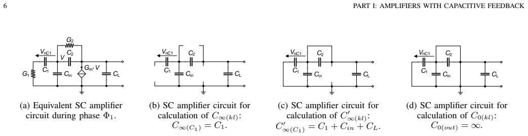
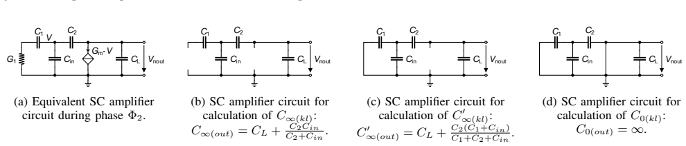
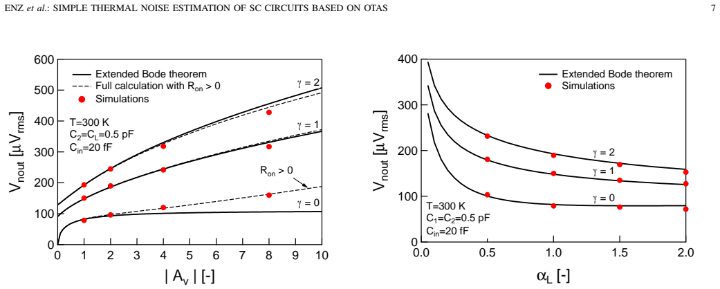
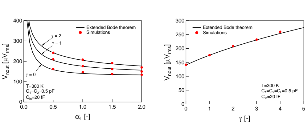
Run a transient-noise simulation of the SC amplifier of Fig. 3 with $C_2=C_L=0.5$ pF, $C_{in}=20$ fF, gain $|A_v|=8$, and a switch resistance raised so that $G_m R_{on}$ is near 1; the $\gamma=0$ switch-only output noise predicted by Eq. (23) will fall increasingly below the simulated value as $R_{on}$ grows, while the full finite-$R_{on}$ calculation tracks the simulation.
Extended reading notes
Core claim
On its own terms, the paper's discovery is an extension of Bode's theorem from passive RLC networks to active OTA-based switched-capacitor circuits. The variance of the thermal noise voltage between any two nodes $k$ and $l$ is claimed to be $V_{n(kl)}^2 = k_B T [1/C_\infty(kl) + (\gamma/h_{fb}-1)/C'_\infty(kl) - (\gamma/h_{fb})/C_0(kl)]$, where $C_\infty$ is the capacitance seen when all switches and OTAs are removed, $C'_\infty$ is the capacitance seen when closed switches are shorted and OTAs removed, $C_0$ is the capacitance seen when switches are shorted and OTA outputs are grounded, and $h_{fb}$ is the feedback voltage gain from the OTA output to its input. The OTA's excess thermal noise beyond that of a passive conductance is accounted for by assigning it a noise temperature $(\gamma/h_{fb}-1)T$. The paper derives closed-form noise variances for the SC amplifier and the track-and-hold circuit from this identity and checks them against transient noise simulations.
Load-bearing premise
The derivation assumes the switch on-resistance is much smaller than the OTA's effective output resistance, $G_m R_{on} \ll 1$, so the OTA input node behaves as a pure capacitive divider and the switches can be shorted in the excess-noise circuit.
Editorial extensions
If this is right
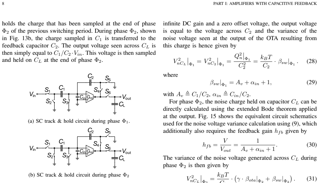
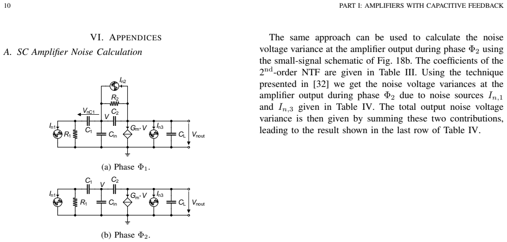
- For the autozero SC amplifier, the total output noise at the end of the amplification phase is $V_{nout}^2 = (k_B T/C_2)(\gamma\beta_{ota}+\beta_{sw})$, with both beta factors explicit ratios of $C_1$, $C_2$, $C_{in}$, and $C_L$, matching the classical transfer-function integration.
- For the SC track-and-hold circuit, the same formula applies with the OTA term coming only from phase 2 and the switch term from both phases; the phase-2 switch contribution is small but is included, refining earlier track-and-hold noise results.
- Because the method needs only capacitance ratios, it directly exposes which capacitors set the sampled noise floor, which is the quantity a low-power designer must trade against capacitance area and settling time.
Reading between the lines
- The paper leaves implicit that the same phase-by-phase three-capacitance recipe should extend to multistage switched-capacitor filters and to each step of a successive-approximation ADC front end, as long as charge transfer between phases is handled the way Part I handles the SC amplifier.
- The paper's stated condition $G_m R_{on} \ll 1$ doubles as a practical error budget: when high-speed designs push the product toward 1, Eq. (9) will under-predict switch noise, and the size of the deviation can be probed by comparing the formula with a nonzero-$R_{on}$ transient simulation.
- A natural but unstated stress test is finite OTA DC gain: the derivation assumes an infinite-gain ideal OTA, so quantifying the correction for low-gain inverter-based amplifiers would be a testable next step.
Signed reviews
Editorial analysis
A structured set of objections, weighed in public.
Referee Report
Summary. This paper proposes a design-oriented method for estimating the thermal noise voltage variance at any port of an OTA-based switched-capacitor circuit during a given clock phase. The method extends Bode's theorem to active circuits by modelling the ideal OTA as a VCCS, replacing it by a conductance Gm·hfb (where hfb is the capacitive feedback gain), splitting the OTA noise into a part consistent with the ambient temperature and an excess-noise part, and applying Bode's theorem to two passive capacitor-only equivalent circuits. The resulting Eq. (9) expresses the variance in terms of three capacitances, C∞, C'∞, and C0, which can be read by inspection. The paper derives closed-form expressions for a SC autozero amplifier and a SC track-and-hold circuit, and compares them with ELDO transient-noise simulations and with the classical transfer-function integration of Appendix VI-A.
Significance. The proposed formula is parameter-free and falsifiable: Eq. (9) is derived algebraically with no fitted parameters, and Appendix VI-A independently reproduces the variances by classical transfer-function integration, which is a definite strength. If the validity conditions are respected, this gives circuit designers a simple, inspection-based alternative to noise PSD integration for an important class of SC circuits. The main caveat is that the derivation rests on ideal-OTA and GmRon<<1 assumptions, and the paper's own simulations show the approximation degrading at GmRon≈0.27; the method is therefore best viewed as an accurate design estimate within a regime that should be quantified.
major comments (2)
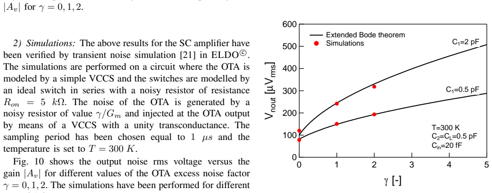
- [Section III, Eqs. (4)-(9) and Fig. 10] The central formula Eq. (9) is derived under the condition Gon >> hfbGm (equivalently GmRon << 1), which is used both to replace the switch conductances by short circuits in Fig. 6(d) and, more fundamentally, to justify the input-node relation V = hfb·Vout in Eq. (4). The paper states this condition but gives no quantitative bound on GmRon for a target accuracy. Fig. 10 shows that for γ=0 the switch-only curve deviates visibly from the full calculation once GmRon reaches about 0.27, and the deviation increases with amplifier gain, so a user of Eq. (9) cannot tell from the stated condition whether the formula is accurate to, say, 5%. The authors should provide a design rule or an approximate correction term for finite GmRon, and should present Eq. (9) as an approximation valid in this regime rather than as an exact equality.
- [Section IV.A.2, Figs. 10-12] The validation in Figs. 10-12 is performed with the same ideal VCCS model of the OTA and the same switch model (ideal switch plus series resistor Ron) that is used in the derivation, so the agreement demonstrates internal consistency between Eq. (9) and the classical transfer-function integration of Appendix VI-A, but it does not independently confirm the method for real OTAs with finite output conductance and finite DC gain. Since the abstract and conclusion claim applicability to OTA-based SC circuits without these qualifications, the authors should either add a transistor-level verification or explicitly scope the claim to ideal transconductance amplifiers with GmRon << 1.
minor comments (4)
- [Abstract and Conclusion] The abstract and conclusion state that the method allows 'precise estimation' without carrying the ideal-OTA and GmRon<<1 qualifications; please add these qualifications to avoid overstating the validated regime.
- [Eq. (24b)] There is a duplicated '∼=' in Eq. (24b): the text shows '∼= ∼=αin + ...', which should be a single '∼=' symbol.
- [Section III, before Fig. 5] In the sentence 'The later circuits can now be considered as passive', 'later' should be 'latter'.
- [Fig. 10 and Section IV.A.2] The caption and text refer to 'Full calculation with Ron > 0' and 'Simulations Ron > 0'; please clarify that the dashed lines are the classical analytical expressions including nonzero GmRon rather than a separate simulator result.
Circularity Check
No significant circularity: the central Eq. (9) is derived from the external Bode theorem via explicit network transformations and is cross-checked against classical noise integration and transient-noise simulations, with no fitted parameter as an input.
full rationale
The central result Eq. (9) is obtained in Section III by replacing the ideal-OTA VCCS with an equivalent conductance Gm·h_fb, splitting the OTA noise source into a thermal part at temperature T and an excess part at (γ/h_fb − 1)T, and applying the standard Bode theorem (Eqs. (1)–(3), from Bode 1945) to the resulting passive capacitor-only subcircuits. Each capacitance C∞, C′∞, and C0 is defined by the usual sZ(s) limits, and the derivation is written out in the paper rather than imported as a conclusion. The results are then independently re-derived by classical transfer-function/noise-bandwidth integration in Appendix VI-A (Tables II and IV), and Eqs. (11) and (16) are stated to be identical to those classical expressions. The only self-citations ([33], [40]) are used for context or as limit checks, not as the justification for Eq. (9), so they are not load-bearing. The Gm·Ron << 1 assumption used to short the switch conductances in Fig. 6(d) is a validity condition, explicitly acknowledged in the discussion of Fig. 10 and in footnote 1 of Section IV.A.2; it limits accuracy but does not make the prediction an input. Transient-noise simulations use the same ideal VCCS model as the derivation, which confirms internal consistency rather than a fitted match. No parameter is fitted to force agreement, and no prediction is defined in terms of the target variance. Score 1 reflects only the negligible self-referentiality of validating an ideal-OTA model with an ideal-OTA simulator; there is no circular step.
Assumptions & free parameters
assumptions (6)
- standard math Bode theorem for passive RLC networks: total noise variance equals kT(1/C_infinity - 1/C_0).
- domain assumption Thermal noise sources are white with PSD 4kBT/R for switches and 4kBT gamma Gm for the OTA.
- domain assumption OTA is ideal: infinite DC gain, zero offset, infinite input impedance, modeled as a VCCS.
- domain assumption Switch on-resistances are much smaller than the inverse OTA transconductance (Gm Ron << 1, Gon >> h_fb Gm).
- domain assumption Noise during each clock phase is stationary and is frozen at the switching instant.
- domain assumption Flicker (1/f) noise is negligible or eliminated by autozeroing.
Cite this review
Pith. "Pith review of Simple Thermal Noise Estimation of Switched Capacitor Circuits Based on OTAs -- Part I: Amplifiers with Capacitive Feedback." pith.science (2026). https://pith.science/paper/DAIFSGLB
@misc{pith2026190808099,
  author       = {Pith},
  title        = {Pith review of: Simple Thermal Noise Estimation of Switched Capacitor Circuits Based on OTAs -- Part I: Amplifiers with Capacitive Feedback},
  year         = {2026},
  howpublished = {\url{https://pith.science/paper/DAIFSGLB}},
  note         = {Machine review of arXiv:1908.08099}
}
read the original abstract
This paper presents a simple method for estimating the thermal noise voltage variance in passive and active switched-capacitor (SC) circuits using operational transconductance amplifiers (OTA). The proposed method is based on the Bode theorem for passive network which is extended to active circuits based on OTAs with capacitive feedback. It allows for a precise estimation of the thermal noise voltage variance by simple inspection of three equivalent circuits avoiding the calculation of any transfer functions nor integrals. In this Part I, the method is applied to SC amplifiers and track&hold circuits and successfully validated by means of transient noise simulations. Part II extends the application of the method to integrators and active SC filters.
Figures

Figures from the paper (12 more)
Reference graph
Works this paper leans on
-
[33]
Simple Thermal Noise Estimation of OTA-based Switched-capacitor Filters,
C. Enz, F. Krummenacher, and A. Boukhayma, “Simple Thermal Noise Estimation of OTA-based Switched-capacitor Filters,” in 2015 Interna- tional Conference on Noise and Fluctuations (ICNF) , June 2015, pp. 1–4
2015
-
[40]
An Accurate kTC Noise Analysis of CDS Circuits,
A. Caizzone, A. Boukhayma, and C. Enz, “An Accurate kTC Noise Analysis of CDS Circuits,” in 2018 16th IEEE International New Circuits and Systems Conference (NEWCAS) , June 2018, pp. 22–25
work page 2018
-
[41]
Thermal Noise in Track-and-Hold Circuits: Analysis and Simulation Techniques,
B. Murmann, “Thermal Noise in Track-and-Hold Circuits: Analysis and Simulation Techniques,” IEEE Solid-State Circuits Magazine , vol. 4, no. 2, pp. 46–54, Spring 2012. ENZ et al.: SIMPLE THERMAL NOISE ESTIMATION OF SC CIRCUITS BASED ON OTAS 13 Christian Enz (M84, S’12) received the M.S. and Ph.D. degrees in Electrical Engineering from the EPFL in 1984 and...
work page 2012
-
[1]
Frequenzfilterung durch Netzwerke mit periodisch gesteuerten Schaltern,
W. Poschenrieder, “Frequenzfilterung durch Netzwerke mit periodisch gesteuerten Schaltern,” in Proc. NTG-Symp. Analyse und Synthese von Netzwerken, Stuttgart, 1966, pp. 221–237
work page 1966
-
[2]
D. L. Fried, “Analog Sample-data filters,” IEEE Journal of Solid-State Circuits, vol. 7, no. 4, pp. 302–304, Aug. 1972
work page 1972
-
[3]
Gregorian and G
R. Gregorian and G. C. Temes, Analog MOS Integrated Circuits for Signal Processing. Wiley, 1986
1986
-
[4]
All-MOS Charge Redistribution Analog- to-digital Conversion Techniques - Part I,
J. L. McCreary and P. R. Gray, “All-MOS Charge Redistribution Analog- to-digital Conversion Techniques - Part I,” IEEE Journal of Solid-State Circuits, vol. 10, no. 6, pp. 371–379, Dec. 1975
work page 1975
-
[5]
Design of Active N-Path Filters,
M. Darvishi, R. v. d. Zee, and B. Nauta, “Design of Active N-Path Filters,” IEEE Journal of Solid-State Circuits, vol. 48, no. 12, pp. 2962– 2976, 2013
work page 2013
Show all 42 references
-
[6]
Tunable High-Q N-Path Band-Pass Filters: Modeling and Verification,
A. Ghaffari, E. A. M. Klumperink, M. C. M. Soer, and B. Nauta, “Tunable High-Q N-Path Band-Pass Filters: Modeling and Verification,” IEEE Journal of Solid-State Circuits, vol. 46, no. 5, pp. 998–1010, May 2011
2011
-
[7]
A Switched-Capacitor RF Front End With Embedded Programmable High-Order Filtering,
Y . Xu and P. R. Kinget, “A Switched-Capacitor RF Front End With Embedded Programmable High-Order Filtering,” IEEE Journal of Solid- State Circuits, vol. 51, no. 5, pp. 1154–1167, May 2016
2016
-
[8]
A Sub-0.5 Electron Read Noise VGA Image Sensor in a Standard CMOS Process,
A. Boukhayma, A. Peizerat, and C. Enz, “A Sub-0.5 Electron Read Noise VGA Image Sensor in a Standard CMOS Process,” IEEE Journal of Solid-State Circuits , vol. 51, no. 9, pp. 2180–2191, Sept. 2016
2016
-
[9]
A Low-noise CMOS THz Imager Based on Source Modulation and an In-pixel High- Q Passive Switched-capacitor n-path Filter,
A. Boukhayma, A. Dupret, J.-P. Rostaing, and C. Enz, “A Low-noise CMOS THz Imager Based on Source Modulation and an In-pixel High- Q Passive Switched-capacitor n-path Filter,” Sensors, vol. 16, no. 3, March 2016
2016
-
[10]
A Correlated Multiple Sam- pling Passive Switched Capacitor Circuit for Low Light CMOS Image Sensors,
A. Boukhayma, A. Peizerat, and C. Enz, “A Correlated Multiple Sam- pling Passive Switched Capacitor Circuit for Low Light CMOS Image Sensors,” in 2015 International Conference on Noise and Fluctuations (ICNF), June 2015, pp. 1–4
2015
-
[11]
Exact analysis of switched capacitor circuits with arbitrary inputs,
M. Liou and Y .-L. Kuo, “Exact analysis of switched capacitor circuits with arbitrary inputs,” IEEE Transactions on Circuits and Systems , vol. 26, no. 4, pp. 213–223, April 1979
1979
-
[12]
The adjoint switched capacitor network and its application to frequency, noise and sensitivity analysis,
J. Vandewalle, H. D. Man, and J. Rabaey, “The adjoint switched capacitor network and its application to frequency, noise and sensitivity analysis,” International Journal of Circuit Theory and Applications , vol. 9, no. 1, pp. 77–88, Jan. 1981
1981
-
[13]
Noise sources and calculation techniques for switched capacitor filters,
J. H. Fischer, “Noise sources and calculation techniques for switched capacitor filters,” IEEE Journal of Solid-State Circuits , vol. 17, no. 4, pp. 742–752, 1982
1982
-
[14]
Noise Analysis of Switched Capacitor Networks,
C. A. Gobet and A. Knob, “Noise Analysis of Switched Capacitor Networks,” IEEE Trans. on Circuits and Systems , vol. 30, no. 1, pp. 37–43, Jan. 1983
1983
-
[15]
Exact Noise Analysis of SC Circuits and an Approximate Computer Implementation,
J. Goette and C. A. Gobet, “Exact Noise Analysis of SC Circuits and an Approximate Computer Implementation,” IEEE Trans. on Circuits and Systems, vol. 36, no. 4, pp. 508–521, April 1989
1989
-
[16]
Exact noise analysis of ’ideal’ SC networks,
L. Toth and K. Suyama, “Exact noise analysis of ’ideal’ SC networks,” in 1991., IEEE International Sympoisum on Circuits and Systems , 11-14 June 1991 1991, pp. 1585–1588 vol.3
1991
-
[17]
Noise analysis of ideal switched- capacitor networks,
L. Toth, I. Yusim, and K. Suyama, “Noise analysis of ideal switched- capacitor networks,” IEEE Transactions on Circuits and Systems I: Fundamental Theory and Applications , vol. 46, no. 3, pp. 349–363, March 1999
1999
-
[18]
Numerical algorithm for noise analysis of switched-capacitor networks,
O. Oliaei, “Numerical algorithm for noise analysis of switched-capacitor networks,” IEEE Transactions on Circuits and Systems I: Fundamental Theory and Applications , vol. 50, no. 7, pp. 865–876, July 2003
2003
-
[19]
A time-domain technique for computation of noise- spectral density in linear and nonlinear time-varying circuits,
V . Vasudevan, “A time-domain technique for computation of noise- spectral density in linear and nonlinear time-varying circuits,” IEEE Transactions on Circuits and Systems I: Regular Papers , vol. 51, no. 2, pp. 422–433, 2004
2004
-
[20]
Computation of the average and harmonic noise power-spectral density in switched-capacitor circuits,
V . Vasudevan and M. Ramakrishna, “Computation of the average and harmonic noise power-spectral density in switched-capacitor circuits,” IEEE Transactions on Circuits and Systems I: Regular Papers , vol. 51, no. 11, pp. 2165–2174, Nov. 2004
2004
-
[21]
A New Approach for Noise Simulation in Transient Analysis,
P. Bolcato and R. Poujois, “A New Approach for Noise Simulation in Transient Analysis,” in Proc. of the IEEE International Symposium on Circuits and Systems (ISCAS) , vol. 2, May 1992, pp. 887–890
1992
-
[22]
Spectral Distribution of a Sampled 1st-order Lowpass Filtered White Noise,
C. A. Gobet, “Spectral Distribution of a Sampled 1st-order Lowpass Filtered White Noise,” Electronics Letters, vol. 17, no. 19, pp. 720–721, Sept. 1981
1981
-
[23]
Circuit Techniques for Reducing the Effects of Op-amp Imperfections: Autozeroing, Correlated Double Sampling, and Chopper Stabilization,
C. C. Enz and G. C. Temes, “Circuit Techniques for Reducing the Effects of Op-amp Imperfections: Autozeroing, Correlated Double Sampling, and Chopper Stabilization,” Proceedings of the IEEE , vol. 84, no. 11, pp. 1584–1614, Nov. 1996
1996
-
[24]
A MOS Switched-capacitor Instrumentation Amplifier,
R. C. Yen and P. R. Gray, “A MOS Switched-capacitor Instrumentation Amplifier,” IEEE Journal of Solid-State Circuits , vol. 17, no. 6, pp. 1008–1013, Dec. 1982
1982
-
[25]
Micropower Switched Capacitor Biquadratic Cell,
F. Krummenacher, “Micropower Switched Capacitor Biquadratic Cell,” IEEE Journal of Solid-State Circuits , vol. 17, no. 3, pp. 507–512, June 1982
1982
-
[26]
Analysis of low-frequency noise reduction by autozero tech- nique,
C. Enz, “Analysis of low-frequency noise reduction by autozero tech- nique,” Electronics Letters, vol. 20, no. 23, pp. 959–960, 1984
1984
-
[27]
A low-noise chopper-stabilized differential switched-capacitor filtering technique,
K.-C. Hsieh, P. R. Gray, D. Senderowicz, and D. G. Messerschmitt, “A low-noise chopper-stabilized differential switched-capacitor filtering technique,” IEEE Journal of Solid-State Circuits , vol. 16, no. 6, pp. 708–715, Dec. 1981
1981
-
[28]
A CMOS chopper amplifier,
C. C. Enz, E. A. Vittoz, and F. Krummenacher, “A CMOS chopper amplifier,” IEEE Journal of Solid-State Circuits, vol. 22, no. 3, pp. 335– 342, June 1987
1987
-
[29]
Performance Limitations in Switched-capacitor Filters,
R. Castello and P. Gray, “Performance Limitations in Switched-capacitor Filters,” IEEE Transactions on Circuits and Systems , vol. 32, no. 9, pp. 865–876, Sept. 1985
1985
-
[30]
W. A. Gardner, Introduction to Random Processes: With Applications to Signals and Systems , New York, 1989
1989
-
[31]
Design-oriented Estimation of Thermal Noise in Switched-capacitor Circuits,
R. Schreier, J. Silva, J. Steensgaard, and G. C. Temes, “Design-oriented Estimation of Thermal Noise in Switched-capacitor Circuits,” IEEE Transactions on Circuits and Systems I: Regular Papers, vol. 52, no. 11, pp. 2358–2368, Nov. 2005
2005
-
[32]
Calculation of Total Integrated Noise in Analog Circuits,
A. Dastgheib and B. Murmann, “Calculation of Total Integrated Noise in Analog Circuits,” IEEE Transactions on Circuits and Systems I , vol. 55, no. 10, pp. 2988–2993, Nov. 2008
2008
-
[34]
H. W. Bode, Network Analysis and Feedback Amplifier Design . New York: van Nostrand Company, 1945
1945
-
[35]
Equivalent Noise Sources of Switched-Capacitor Ele- ments,
H. Weinrichter, “Equivalent Noise Sources of Switched-Capacitor Ele- ments,” in Proc. of the IEEE International Symposium on Circuits and Systems (ISCAS), Rome, May 1982, pp. 38–41
1982
-
[36]
Rauschen von Filtern mit geschalteten Kapazit ¨aten,
B. Furrer, “Rauschen von Filtern mit geschalteten Kapazit ¨aten,” PhD, ETHZ, Date 1983, no. 7284
1983
-
[37]
High voltage gain CMOS OTA for micropower SC filters,
F. Krummenacher, “High voltage gain CMOS OTA for micropower SC filters,” Electronics Letters, vol. 17, no. 4, pp. 160–162, 1981
1981
-
[38]
P. R. Gray, P. J. Hurst, S. H. Lewis, and R. G. Meyer, Analysis and Design of Analog Integrated Circuits , 5th ed. Wiley, 2009
2009
-
[39]
Class AB CMOS amplifier micropower SC filters,
F. Krummenacher, E. Vittoz, and M. Degrauwe, “Class AB CMOS amplifier micropower SC filters,” Electronics Letters , vol. 17, no. 13, pp. 433–435, 1981
1981
-
[2015]
at the Ecole Polytechnique Federale de Lausanne (EPFL), under the supervision of Prof
He is currently working toward the Ph.D. at the Ecole Polytechnique Federale de Lausanne (EPFL), under the supervision of Prof. Enz and Dr. Boukhayma, on the subject of ultra-low noise and low power sensors for healthcare. Between 2012 and 2013 he worked in STMicroelectronics ...
2012
Reviewed August 14, 2026 · model on record in the stance chip above.
Discussion (0). Continue with ORCID to comment.