REVIEW 3 major objections 5 minor 25 references
Inverse-Designed Tapers for Compact Conversion Between Single-Mode and Wide Waveguides
T0 review · 3 major / 5 minor · reviewed 2026-08-12 · deepseek-v4-flash
Pith's one-line read Inverse-designed L-taper converts between single-mode and wide waveguides in a footprint 12 times smaller than a linear taper.
desk verdict New 90-degree 'L-taper' geometry is worth attention, but the headline numbers rest on a single coarse-grid simulation and need a convergence check before being taken as real. read the letter →
The pith
A machine-rendered reading of the paper's core claim, the machinery that carries it, and where it could break.
The reading
What carries the argument
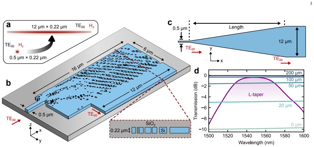
The central object is the L-taper: a topology-optimized transition in which the input and output waveguides meet at a 90-degree angle, so the single-mode input faces a 16 µm by 6 µm design region that acts like a grating coupler bent into the chip plane. The design is parameterized by roughly 350,000 density pixels that evolve under gradient-based topology optimization, with a filter-threshold projection pushing the geometry toward binary, fabricable states and a 50 nm minimum feature size enforced by geometric constraints. The figure of merit is the mode-overlap transmission at 1540, 1550, and 1560 nm, and gradients are computed with an adjoint-variable method. The efficient working mechanism is the resulting set of apodized slanted gratings, which rapidly expands the wavefront; the comparison benchmark is the linear taper, whose required length for equal transmission establishes the 12x footprint reduction.
What would settle it
Re-simulate the optimized geometry at 60 or 120 voxels per micron, or fabricate it on 220 nm SOI and measure its transmission spectrum. If the peak transmission and 1-dB bandwidth change materially—for example, if -0.38 dB and 40 nm are not reproduced at higher resolution—then the claim of a 12x smaller footprint with equal transmission would fail.
Extended reading notes
Core claim
The central discovery is that rotating the input and output waveguides 90 degrees relative to each other transforms the waveguide-taper problem into an in-plane grating-coupler problem that topology optimization can solve with near-unity efficiency in a footprint only slightly larger than the wide waveguide itself. The optimized structure, an arrangement of apodized slanted gratings in a 16 µm by 6 µm design region, reaches -0.38 dB conversion from the TE00 mode of a 0.5 µm waveguide to the TE00 mode of a 12 µm waveguide on a 220 nm SOI platform, with 40 nm 1-dB bandwidth centered at 1547 nm and mode suppression greater than 14 dB for the first five higher-order TE modes across 1540-1560 nm. This matches the peak transmission of a 100 µm long linear taper, whose footprint is 12 times larger. The authors further claim that the same technique can reach arbitrarily wide waveguides, can be set to excite a chosen higher-order mode or phase profile, and is compatible with standard fabrication constraints and material platforms.
Load-bearing premise
The load-bearing premise is that the finite-difference time-domain simulation used to evaluate the final design, run at 30 voxels per micron without a grid-convergence check or experimental verification, accurately resolves the structure's 50 nm features and therefore the reported -0.38 dB transmission and 40 nm bandwidth.
Editorial extensions
If this is right
- If the simulated performance holds, single-mode to wide-waveguide conversion on SOI shrinks from a 1200 µm² linear taper to a 96 µm² L-taper, which directly increases the packing density of photonic circuits.
- Because the L-taper turns the optical path by 90 degrees, it can serve as both a taper and a corner bend, saving additional layout area beyond the 12x footprint comparison.
- The same topology-optimization formulation can be adapted to other waveguide widths, material platforms, and design rules, including designs that launch a specific higher-order mode or an arbitrary phase profile in the wide waveguide.
- The demonstrated 40 nm 1-dB bandwidth centered at 1547 nm is sufficient for conventional telecom applications, so the device is positioned for C-band communications.
Reading between the lines
- The 12x claim compares footprints at equal peak transmission; if the comparison were made at equal 1-dB bandwidth, the linear taper's much flatter spectral response could make the L-taper's advantage smaller, since the grating-like L-taper is inherently more narrowband.
- The reported results are purely simulated, so a foundry fabrication run followed by spectral measurement is the natural test: if the 50 nm features are not faithfully reproduced, the measured insertion loss and bandwidth will likely differ from -0.38 dB and 40 nm.
- Because the design region and wide-waveguide width are linked, extending the approach to wider targets such as tens of microns may require a larger grating region or a multi-stage design; the paper's 'arbitrarily wide' claim is plausible but not yet demonstrated beyond 12 µm.
Editorial analysis
A structured set of objections, weighed in public.
Referee Report
Summary. The paper proposes a topology-optimized "L-taper" that connects a 0.5-µm single-mode waveguide to a 12-µm wide waveguide on 220 nm SOI, with the input and output waveguides rotated 90° relative to each other. The design region is 16 µm × 6 µm, optimized via density-based topology optimization with FDTD and adjoint gradients. The optimized design is reported to achieve −0.38 dB peak transmission at 1547 nm and 40 nm 1-dB bandwidth, corresponding to a footprint 12× smaller than a 100-µm linear taper of similar peak transmission. The paper also compares higher-order mode excitation in the L-taper and a 100-µm linear taper.
Significance. If the reported performance is reliable, the L-taper offers a compact, fabrication-rule-compliant solution for mode conversion from a single-mode to a wide waveguide, with clear applications in grating couplers and high-power photonics. Rotating the waveguides by 90° to create an in-plane, grating-coupler-like taper is a conceptually neat idea that could substantially improve device packing density. The authors use standard open-source tools (Meep) and include a 50-nm minimum feature constraint, which are strengths. However, all quantitative claims rest on a single simulation evaluation at a coarse 30-voxel/µm grid, with no grid-convergence study or experimental validation; the reported metrics are the optimizer's own objective values. The central claim is therefore not yet established at the level required for a journal publication.
major comments (3)
- [Section II] The manuscript states in Section II that "The design was simulated at a resolution of 30 voxels/µm, and the optimization was performed with a resolution of 60 voxels/µm." All reported metrics—the −0.38 dB peak transmission, the 40 nm 1-dB bandwidth, and the 12× footprint comparison in Section III-A—are obtained from the 30-voxel/µm evaluation. Since the minimum feature size is 50 nm, this grid gives only ~1.5 cells per feature, and FDTD staircasing or under-resolution may significantly alter both the transmission and the bandwidth. Please add a grid-convergence study (e.g., evaluations at 60 and 90 voxels/µm) or provide a quantitative justification of why 30 voxels/µm is sufficient. This is load-bearing for every headline number.
- [Section II, Eq. (2)] The reported performance is the direct figure of merit of the optimization: Eq. (2) defines the FOM as the mode-overlap transmission in dB, and the paper reports the value after 490 iterations of maximizing that FOM. This makes the −0.38 dB and 40 nm bandwidth in-sample objective values, not independent or out-of-sample predictions. To support the central claim, the authors should report a transmission spectrum obtained from an independent, fine-grid simulation (and ideally a fabricated device), and clearly distinguish optimized objective values from validated performance.
- [Section III-A, Fig. 2(d)] The comparison to a 100-µm linear taper appears to be based on peak transmission at 1547 nm, but the text does not specify at which wavelength(s) the linear tapers are evaluated in Fig. 2(d). Given that the text says linear tapers have "significantly larger bandwidth," a peak-transmission-only comparison does not fully capture the trade-off between the compact L-taper and the broadband linear taper. Please specify the evaluation wavelengths for both devices and, if appropriate, report the bandwidth together with the peak transmission for each design.
minor comments (5)
- [Abstract and Section IV] The abstract and conclusion use "demonstrate" for results that are entirely simulation-based; a wording such as "we design and simulate" would be more accurate.
- [Section II] The filter-threshold projection and the minimum feature size constraints (g1 and g2 in Eq. (1)) are only cited to Ref. [20]; a brief self-contained description would improve reproducibility.
- [Section II] The text says the symmetry plane "halved the computation complexity"; this likely means halved the computational domain, and the wording should be clarified.
- [Section II] No convergence plot or optimization trajectory is shown; a figure of the FOM versus iteration would support the claim that the design converged after 490 iterations.
- [Section III-B] The acronym "MSR" (mode suppression ratio) should be defined in the text at its first use in Section III-B, not only in the caption of Fig. 3.
Circularity Check
No significant circularity; the reported transmission is the optimization objective, but the paper presents it as an optimization outcome and the bandwidth/modal claims rest on separate simulations.
full rationale
No circularity found in the paper's derivation chain. The device is produced by density-based topology optimization, and Eq. (2) defines the figure of merit as the mode-overlap transmission in dB. The optimizer is run at 1540, 1550, and 1560 nm, and the final quoted peak of -0.38 dB at 1547 nm is indeed the objective value achieved by that optimization. However, the paper openly frames this as an optimized design result rather than as an independent prediction, so reporting the objective value is not a hidden circular step. The 40 nm 1-dB bandwidth is evaluated by separate FDTD simulations over a wider wavelength range than the three optimized wavelengths, and the >14 dB mode-suppression ratio is obtained from additional modal-overlap simulations for the first five TE modes; neither is built into the objective. The comparison to a 100 micron linear taper uses an independently simulated interpolation of linear-taper transmission, so the 12x footprint claim is not constructed from the L-taper's own inputs. The self-citations [13], [16], [17], [20] concern solver methodology, parameterization, and fabrication constraints; they are not used as a load-bearing substitute for the performance claim. The grid-resolution mismatch (30 voxels/um for evaluation versus 60 voxels/um for optimization) is a possible correctness risk regarding simulation fidelity, but it is not a circularity: it does not make the claimed result an input to itself.
Assumptions & free parameters
free parameters (5)
- Optimized pixel permittivities (approx. 350,000 variables) =
not provided (optimized geometry)
- Optimization target wavelengths =
1540, 1550, 1560 nm
- Design region dimensions =
16 um x 6 um
- Minimum feature size =
50 nm
- Simulation and optimization resolutions =
30 voxels/um (simulate), 60 voxels/um (optimize)
assumptions (4)
- domain assumption Maxwell's equations solved by FDTD in Meep accurately model the device
- standard math Passive reciprocity holds for the taper
- domain assumption Vertical symmetry plane through the middle of the 220 nm Si layer is valid
- domain assumption Filter-threshold projection yields binary fabricable structures
Cite this review
Pith. "Pith review of Inverse-Designed Tapers for Compact Conversion Between Single-Mode and Wide Waveguides." pith.science (2026). https://pith.science/paper/2GUWDHKY
@misc{pith2026241114309,
  author       = {Pith},
  title        = {Pith review of: Inverse-Designed Tapers for Compact Conversion Between Single-Mode and Wide Waveguides},
  year         = {2026},
  howpublished = {\url{https://pith.science/paper/2GUWDHKY}},
  note         = {Machine review of arXiv:2411.14309}
}
read the original abstract
Waveguide tapers are critical components for leveraging the benefits of both single-mode and wide waveguides. Adiabatic tapers are typically hundreds of microns in length, dramatically limiting density and scalability. We reenvision the taper design process in an inverse-design paradigm, introducing the novel L-taper. We present a novel approach to inverse-designed tapers where the input and output waveguides are rotated 90 degrees with respect to each other. The resultant design has an order-of-magnitude smaller footprint, and the design process is compatible with a variety of fabrication processes. We demonstrate an L-taper designed on 220 nm silicon-on-insulator that converts a 0.5 micron waveguide to a 12 micron waveguide with -0.38 dB transmission and 40 nm 1-dB bandwidth. The footprint is 16 micron by 6 micron, representing a 12x smaller footprint than a linear taper with the same transmission.
Figures


Reference graph
Works this paper leans on
-
[1]
Multilayer platform for ultra-low-loss waveguide applications,
D. D. John, M. J. Heck, J. F. Bauters, R. Moreira, J. S. Barton, J. E. Bowers, and D. J. Blumenthal, “Multilayer platform for ultra-low-loss waveguide applications,” IEEE Photonics Technology Letters , vol. 24, no. 11, pp. 876–878, 2012
work page 2012
-
[2]
Ultra-low loss waveguide platform and its integration with silicon photonics,
M. J. Heck, J. F. Bauters, M. L. Davenport, D. T. Spencer, and J. E. Bowers, “Ultra-low loss waveguide platform and its integration with silicon photonics,” Laser & Photonics Reviews , vol. 8, no. 5, pp. 667– 686, 2014
work page 2014
-
[3]
M. Xiang, Y . Zhang, G. Li, C. Liu, Q. Chen, Q. Lu, L. Huang, M. Lu, J. DoneGan, and W. Guo, “Wide-waveguide high-power low-rin single- mode distributed feedback laser diodes for optical communication,” Opt. Express , vol. 30, no. 17, pp. 30 187–30 197, Aug 2022. [Online]. Available: https://opg.optica.org/oe/abstract.cfm?URI=oe-30-17-30187
work page 2022
-
[4]
Multi- dimensional data transmission using inverse-designed silicon photonics and microcombs,
K. Y . Yang, C. Shirpurkar, A. D. White, J. Zang, L. Chang, F. Ashtiani, M. A. Guidry, D. M. Lukin, S. V . Pericherla, J. Yang et al. , “Multi- dimensional data transmission using inverse-designed silicon photonics and microcombs,” Nature communications, vol. 13, no. 1, p. 7862, 2022
work page 2022
-
[5]
Silicon integrated nanophotonic devices for on-chip multi-mode interconnects,
H. Xu, D. Dai, and Y . Shi, “Silicon integrated nanophotonic devices for on-chip multi-mode interconnects,” Applied Sciences, vol. 10, no. 18, p. 6365, 2020
work page 2020
-
[6]
Compact efficient broadband grating coupler for silicon-on-insulator waveguides,
D. Taillaert, P. Bienstman, and R. Baets, “Compact efficient broadband grating coupler for silicon-on-insulator waveguides,” Optics letters , vol. 29, no. 23, pp. 2749–2751, 2004
work page 2004
-
[7]
Grating couplers on silicon photonics: Design principles, emerging trends and practical issues,
L. Cheng, S. Mao, Z. Li, Y . Han, and H. Fu, “Grating couplers on silicon photonics: Design principles, emerging trends and practical issues,” Micromachines, vol. 11, no. 7, p. 666, 2020
work page 2020
-
[8]
C. Li, D. Liu, and D. Dai, “Multimode silicon photonics,” Nanophoton- ics, vol. 8, no. 2, pp. 227–247, 2019
work page 2019
Show all 25 references
-
[9]
Adiabatic operation slope-loss algorithm for ultrashort and broadband waveguide taper,
T.-L. Liang, X. Cheng, M. Yu, L. Zhang, J. Shi, and W. Shao, “Adiabatic operation slope-loss algorithm for ultrashort and broadband waveguide taper,” Frontiers in Physics , vol. 10, p. 1029359, 2022
2022
-
[10]
Erbium- doped lithium niobate thin film waveguide amplifier with 16 db internal net gain,
M. Cai, K. Wu, J. Xiang, Z. Xiao, T. Li, C. Li, and J. Chen, “Erbium- doped lithium niobate thin film waveguide amplifier with 16 db internal net gain,” IEEE Journal of Selected Topics in Quantum Electronics , vol. 28, no. 3: Hybrid Integration for Silicon Photonics, pp. 1–8, 2022
2022
-
[11]
Ultrashort waveguide tapers based on luneburg lens,
S. H. Badri and M. Gilarlue, “Ultrashort waveguide tapers based on luneburg lens,” Journal of Optics , vol. 21, no. 12, p. 125802, 2019
2019
-
[12]
Ultra-short beam expander with segmented curvature control: the emergence of a semi-lens,
S. Abbaslou, R. Gatdula, M. Lu, A. Stein, and W. Jiang, “Ultra-short beam expander with segmented curvature control: the emergence of a semi-lens,” Opt. Lett. , vol. 42, no. 21, pp. 4383–4386, Nov
-
[13]
Topology optimized integrated sin mode converters,
M. J. Probst, A. M. Hammond, and S. E. Ralph, “Topology optimized integrated sin mode converters,” in 2023 IEEE Photonics Conference (IPC). IEEE, 2023, pp. 1–2
2023
-
[14]
Fast inverse design of 3d nanophotonic devices using boundary integral methods,
E. Garza and C. Sideris, “Fast inverse design of 3d nanophotonic devices using boundary integral methods,” ACS Photonics , vol. 10, no. 4, pp. 824–835, 2022
2022
-
[15]
Leveraging continuous material averaging for inverse electromagnetic design,
A. Michaels and E. Yablonovitch, “Leveraging continuous material averaging for inverse electromagnetic design,” Opt. Express , vol. 26, no. 24, pp. 31 717–31 737, Nov 2018. [Online]. Available: https: //opg.optica.org/oe/abstract.cfm?URI=oe-26-24-31717
2018
-
[16]
High-performance hybrid time/frequency-domain topology optimization for large-scale photonics inverse design,
A. M. Hammond, A. Oskooi, M. Chen, Z. Lin, S. G. Johnson, and S. E. Ralph, “High-performance hybrid time/frequency-domain topology optimization for large-scale photonics inverse design,” Optics Express , vol. 30, no. 3, pp. 4467–4491, 2022
2022
-
[17]
Pho- tonic topology optimization with semiconductor-foundry design-rule constraints,
A. M. Hammond, A. Oskooi, S. G. Johnson, and S. E. Ralph, “Pho- tonic topology optimization with semiconductor-foundry design-rule constraints,” Optics Express, vol. 29, no. 15, pp. 23 916–23 938, 2021
2021
-
[18]
Minimum length scale in topology optimization by geometric constraints,
M. Zhou, B. S. Lazarov, F. Wang, and O. Sigmund, “Minimum length scale in topology optimization by geometric constraints,” Computer Methods in Applied Mechanics and Engineering , vol. 293, pp. 266–282, 2015
2015
-
[19]
Full c-band tunable coherent transmitter and receiver inp photonic integrated cir- cuits,
V . Lal, J. Summers, A. Hosseini, S. Corzine, P. Evans, M. Lauermann, R. Going, A. Nguyen, M. Chitgarha, J. Osenbach et al. , “Full c-band tunable coherent transmitter and receiver inp photonic integrated cir- cuits,” in ECOC 2016-Post Deadline Paper; 42nd European Conference ...
2016
-
[20]
Fabrication tolerant multi-layer integrated photonic topology optimization,
M. J. Probst, A. Khurana, J. B. Slaby, A. M. Hammond, and S. E. Ralph, “Fabrication tolerant multi-layer integrated photonic topology optimization,” Optics Express, vol. 32, no. 18, pp. 31 448–31 462, 2024
2024
-
[21]
Topology optimization approaches,
O. Sigmund and K. Maute, “Topology optimization approaches,” Struc- tural and Multidisciplinary Optimization , vol. 48, no. 6, pp. 1031–1055, 2013
2013
-
[22]
Topology optimization for nano- photonics,
J. S. Jensen and O. Sigmund, “Topology optimization for nano- photonics,” Laser & Photonics Reviews , vol. 5, no. 2, pp. 308–321, 2011
2011
-
[23]
Inverse design in photonics by topology optimization: tutorial,
R. E. Christiansen and O. Sigmund, “Inverse design in photonics by topology optimization: tutorial,” JOSA B , vol. 38, no. 2, pp. 496–509, 2021
2021
-
[24]
MEEP: A flexible free-software package for electromagnetic simulations by the FDTD method,
A. F. Oskooi, D. Roundy, M. Ibanescu, P. Bermel, J. D. Joannopoulos, and S. G. Johnson, “MEEP: A flexible free-software package for electromagnetic simulations by the FDTD method,” Computer Physics Communications, vol. 181, no. 3, pp. 687–702, 2010
2010
-
[2017]
Available: https://opg.optica.org/ol/abstract.cfm?URI= ol-42-21-4383
[Online]. Available: https://opg.optica.org/ol/abstract.cfm?URI= ol-42-21-4383
Reviewed August 12, 2026 · model on record in the stance chip above.
Discussion (0). Continue with ORCID to comment.