REVIEW 3 major objections 5 minor 43 references
Silicon-Enhanced Nanocavity: From Narrow Band Color Reflector to Broadband Near-Infrared Absorber
T0 review · 3 major / 5 minor · reviewed 2026-08-12 · deepseek-v4-flash
Pith's one-line read A five-layer Ti–SiO2–Si–SiO2–Ag stack is claimed to work as both a narrowband color reflector and a broadband near-infrared absorber, with 5 nm of silicon tuning the reflected color.
desk verdict A plausible dual-function thin-film stack with a real measurement gap: the visible color-reflector story mostly holds, but the headline NIR absorption numbers are not actually measured across the full claimed band. read the letter →
The pith
A machine-rendered reading of the paper's core claim, the machinery that carries it, and where it could break.
The reading
What carries the argument
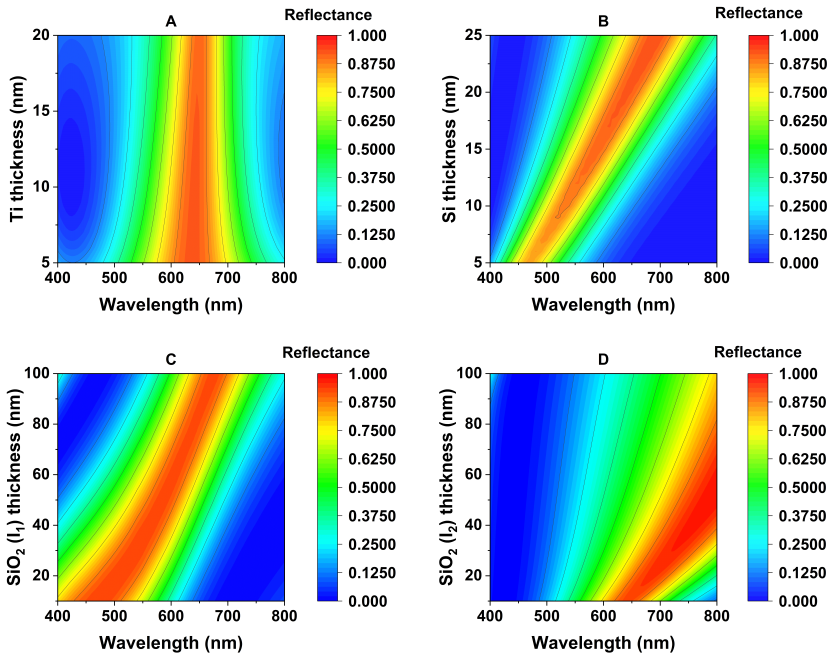
The design's load-bearing element is the dielectric-semiconductor-dielectric spacer (SiO2–Si–SiO2) inside the Ti/Ag asymmetric Fabry–Perot cavity. Because silicon has a high extinction coefficient at short visible wavelengths, it suppresses reflectance there and shortens the cavity enough that a 5 nm change in its thickness produces a large shift of the Fabry–Perot resonance, while its loss reduces the angular sensitivity relative to a pure dielectric spacer. The mechanism is carried by the round-trip phase delay inside the cavity, set to target a 600 nm reflection peak, and the splitting of the stack into a metal-dielectric-semiconductor and semiconductor-dielectric-metal pair that together absorb broadly in the near-infrared.
What would settle it
Fabricate the Ti(10 nm)-SiO2(80 nm)-Si(15 nm)-SiO2(10 nm)-Ag(100 nm) stack and measure absolute reflectance and transmittance with an integrating sphere from 800 to 1300 nm; if the inferred absorptance $A = 1 - R - T$ drops below 80% over that band, or if spectroscopic ellipsometry of the sputtered 15 nm silicon film disagrees significantly with the literature near-infrared constants, the broadband-absorber claim fails.
Extended reading notes
Core claim
The paper's central claim is that inserting a semiconductor into the spacer of an asymmetric Fabry–Perot nanocavity changes the device's character rather than just tuning it. The SiO2–Si–SiO2 sandwich between a 10 nm titanium top layer and a 100 nm silver bottom layer yields a narrowband visible reflector that is highly sensitive to silicon thickness, so 5 nm increments shift the reflection peak across the blue-to-orange range, while the same structure reflects less than 30% of light up to 1600 nm — a broadband absorber. The absorption mechanism is described as the stack splitting into a metal-dielectric-semiconductor section and a semiconductor-dielectric-metal section, with the titanium layer absorbing the most power and the silicon and silver contributing. An 80 nm SiO2 anti-reflection coating further suppresses NIR reflection, giving near-unity absorption in parts of the range with minimal effect on the visible peak.
Load-bearing premise
The predictions depend on the ultrathin sputtered silicon, titanium, and silver films having the refractive indices assumed in the simulations — ellipsometric values for the visible and literature values for the near-infrared — since any deviation shifts the tuning and the absorption numbers.
Editorial extensions
If this is right
- A 5 nm change in the silicon layer shifts the reflected color peak across the visible spectrum, so RGB reflective filters can be fabricated without lithography.
- The same stack absorbs over 80% of incident light from 800 to 1300 nm and over 70% out to 1600 nm, with zero transmittance assumed from the thick silver base.
- An 80 nm SiO2 anti-reflection coating raises the near-infrared absorption toward unity while preserving the visible reflected color.
- The architecture is material-agnostic: any semiconductor with a similar extinction-coefficient trend should reproduce the phase-change and absorption behavior.
- The reduced angular sensitivity means the reflected color remains stable up to 60° incidence, with only a blue shift.
Reading between the lines
- The absorber claim is inferred from reflectance alone (A = 1 − R); a direct absorptance measurement could revise the quoted percentages.
- The demonstrated 5 nm color sensitivity implies tight thickness tolerances in manufacturing — a useful tuning lever, but a control risk.
- The dual function suggests a single large-area device could both display color and harvest near-infrared solar energy, a combination the paper does not explicitly build.
- Choosing semiconductors with absorption edges at other wavelengths could translate the same stack design to other bands, such as short-wave infrared imaging.
Editorial analysis
A structured set of objections, weighed in public.
Referee Report
Summary. The manuscript proposes a planar, lithography-free Ti-SiO2-Si-SiO2-Ag asymmetric Fabry-Perot nanocavity, with an optional SiO2 anti-reflection coating, that is claimed to act simultaneously as a narrowband visible color reflector and a broadband near-infrared absorber. The design is developed with transfer-matrix and FDTD simulations, and samples with Si thicknesses of 5, 10, and 20 nm are fabricated and characterized. The reported visible reflectance spectra show color peaks that shift with Si thickness, and the NIR reflectance measurements over 970-1640 nm are compared with simulations. The central quantitative claims are that absorption exceeds 70% over 800-1600 nm (abstract), that absorption exceeds 80% over 800-1300 nm (conclusion), and that the AR coating extends near-unity absorption toward 1600 nm.
Significance. If the quantitative absorption claims are fully supported, the work demonstrates a useful dual-function planar stack: a narrowband reflective color filter whose peak can be tuned by a few nanometers of Si thickness, and a broadband NIR absorber, both without nanopatterning. The use of abundant silicon, standard sputtering, and a simple multilayer geometry gives the design practical appeal for displays and thermal photovoltaics. Strengths of the paper include the explicit TMM/FDTD design procedure, the fabrication of the proposed structures, the direct visible reflectance measurements with angle- and polarization-resolved data, and the clear qualitative agreement between measured and simulated spectra. However, the quantitative NIR absorption figures are not yet empirically established over the full claimed bandwidth, because the measurement setup and spectral coverage do not directly support them.
major comments (3)
- [Results and discussion, Figure 9] The claimed broadband absorption over 800-1600 nm (abstract) and 800-1300 nm (conclusion) is not experimentally established, because the reported NIR spectrometer covers only 970-1640 nm while the visible spectrometer covers 200-830 nm, leaving the entire 830-970 nm range unmeasured. The authors assert that this gap 'does not impact the research objectives,' but that assertion is not supported: 800-970 nm is precisely the transition region between the visible color-reflection regime and the NIR absorbing regime, and it is where the silicon extinction coefficient changes most rapidly. The quantitative thresholds (70% and 80%) therefore rest on an interpolation across the very band where the device behavior is expected to change. The manuscript should either extend the NIR reflectance measurement down to 800 nm or explicitly restrict the claims to the measured range.
- [Experimental and Simulation Methods; Structure Modeling] Absorption is inferred, not measured. The reflectance data are obtained with a normal reflection/backscattering probe normalized to a thick Ag-coated reference, rather than with a calibrated integrating-sphere measurement, and transmittance is never measured. In the Structure Modeling section, the relation A = 1 - R is used with the statement that transmittance is zero, but no transmission check is reported for the fabricated films, nor is there a discussion of scattered light or the angular collection efficiency of the probe. Without a hemispherical reflectance measurement and a transmittance measurement (or an alternative direct absorptance measurement), the quantitative absorption values of 'over 70%,' 'over 80%,' and 'near unity' are not empirically supported. At minimum, the manuscript should report uncertainty bars, raw reflectance spectra, and a transmittance measurement for the representative stacks.
- [Experimental and Simulation Methods; Results and discussion] The reliability of the NIR optical constants used in the TMM and FDTD predictions is a significant correctness risk. For the NIR range, the refractive indices of Ag, SiO2, Si, and Ti are taken from literature values for thin films or bulk-like samples (Ciesielski et al., Gao et al., Pierce et al., Palm et al.), while the fabricated Si, Ti, and SiO2 layers are ultrathin sputtered films that may differ in microstructure, density, oxidation, or interface quality. The manuscript itself notes in Results and discussion that the measured visible reflectance spectra show broadening attributed to 'variations in the number density and damping factor within the silicon layer.' A concrete validation step would be to measure the optical constants of the deposited films across the full 400-1600 nm range, or to perform a sensitivity analysis showing how the predicted 800-1600 nm absorption changes for plausible variations in n and k. This is a correctness concern, not a circularity concern, and it directly affects the quantitative tuning and absorption claims.
minor comments (5)
- [Introduction] There are typographical errors, including 'realtively' (should be 'relatively') and 'Danton' (should be 'Denton').
- [Figure 4 caption] The caption lists structure (E) as 'Si (5 nm)' but the accompanying text describes it as a 25 nm Si layer; the caption should be corrected to match the intended thickness.
- [Results and discussion, Figure 9] The statement that the 830-970 nm data gap 'does not impact the research objectives' is presented without support; even if the visible and NIR regimes are separately of interest, the gap breaks the continuity of the claimed broadband absorption spectrum.
- [Structure Modeling, Figure 5] The comparison with the Shurvinton et al. MDM cavity is useful, but the text should clarify whether the plotted absorptance for that structure is also inferred as A = 1 - R and whether the same zero-transmittance assumption applies.
- [Conclusions] The abstract and conclusion quote different absorption thresholds (over 70% over 800-1600 nm versus over 80% over 800-1300 nm); the inconsistency should be reconciled and each claim tied to the specific spectral range that is actually measured.
Circularity Check
The derivation is self-contained: the design uses TMM parameter sweeps to choose layer thicknesses, then validates the chosen structures by fabrication and reflectance measurement; no prediction reduces to a fitted input.
full rationale
No significant circularity was found. The paper's central claims are that the Ti-SiO2-Si-SiO2-Ag stack produces narrowband visible reflection tunable with silicon thickness and broadband NIR absorption, and that an additional SiO2 anti-reflection coating improves the NIR absorption. The design thicknesses are selected from TMM contour plots (Figures 2 and 6) that scan Si, Ti, and SiO2 thicknesses; this is a standard parameter sweep for design, not a fit of a prediction target. The fabricated samples use the chosen thicknesses, and the measured visible reflectance spectra are compared with the modeled spectra rather than being forced by construction to match them. In the NIR, the paper reports measured reflectance spectra over 970-1640 nm and compares them with TMM/FDTD simulations; the 830-970 nm gap is acknowledged but does not make the NIR reflectance a fitted input. The absorptance is inferred as A = 1 - R assuming zero transmittance owing to the optically thick Ag bottom layer; that is a physical assumption, not circular reasoning. The self-citations (refs. 5, 9, 21, 25, 29) are used as background or motivation, and the quantitative results are obtained from TMM/FDTD calculations and the paper's own measurements, not from those cited papers. No load-bearing equation reduces a prediction to a fitted parameter, and no central claim is equivalent to its input by definition.
Assumptions & free parameters
free parameters (5)
- Ti layer thickness =
10 nm
- Top SiO2 thickness =
80 nm
- Bottom SiO2 thickness =
10 nm
- Si thickness =
5, 10, 20 nm (fabricated); 5-25 nm (simulated)
- AR coating SiO2 thickness =
80 nm
assumptions (4)
- domain assumption Optical constants from ellipsometry (visible) and literature (NIR) are representative of the actual deposited films.
- domain assumption The 100 nm Ag layer blocks all transmission, so absorptance equals 1 minus reflectance.
- domain assumption TMM and FDTD with periodic boundary conditions accurately model the planar multilayer structure, ignoring roughness, intermixing, and oxidation.
- standard math Standard Maxwell-equation solvers (TMM/FDTD) are valid for these subwavelength multilayer stacks.
Cite this review
Pith. "Pith review of Silicon-Enhanced Nanocavity: From Narrow Band Color Reflector to Broadband Near-Infrared Absorber." pith.science (2026). https://pith.science/paper/JOOL5N7R
@misc{pith2026241115313,
  author       = {Pith},
  title        = {Pith review of: Silicon-Enhanced Nanocavity: From Narrow Band Color Reflector to Broadband Near-Infrared Absorber},
  year         = {2026},
  howpublished = {\url{https://pith.science/paper/JOOL5N7R}},
  note         = {Machine review of arXiv:2411.15313}
}
read the original abstract
Subwavelength-scale light absorbers and reflectors have gained significant attention for their potential in photonic applications. These structures often utilize a metal-insulator-metal (MIM) architecture, similar to a Fabry-Perot nanocavity, using noble metals and dielectric or semiconductor spacers for narrow-band light absorption. In reflection mode, they function as band-stop filters, blocking specific wavelengths and reflecting others through Fabry-Perot resonance. Efficient color reflection requires asymmetric Fabry-Perot cavities, where metals with differing reflectivities and extinction coefficients enable substantial reflection for non-resonant wavelengths and near-perfect absorption at resonant ones. Unlike narrowband techniques, broadband absorption does not rely on a single resonance phenomenon. Recent developments show that integrating an asymmetric Fabry-Perot nanocavity with an anti-reflection coating achieves near-unity absorption across a broad wavelength range. This study introduces an asymmetric Fabry-Perot nanocavity with a dielectric-semiconductor-dielectric spacer, enabling near-unity color reflection. By incorporating silicon, the reflected color can be tuned with just a 5 nm thickness variation, while achieving broadband absorption over 70% in the 800-1600 nm range. The addition of an anti-reflection coating extends broadband absorption to near unity with minimal impact on reflected color. The planar, nanopattern-free design holds promise for display technologies with better color fidelity and applications in thermal photovoltaics.
Figures


Figures from the paper (6 more)


Reference graph
Works this paper leans on
-
[1]
A.; Blanchard, R.; Genevet, P.; Capasso, F
Kats, M. A.; Blanchard, R.; Genevet, P.; Capasso, F. Nanometre optical coatings based on strong interference effects in highly absorbing media. Nature materials 2013, 12, 20--24
work page 2013
-
[2]
High-Chroma Color Coatings Based on Ag/SiO2/Ti/SiO2 Structures
Shurvinton, R.; Lemarchand, F.; Moreau, A.; Lumeau, J. High-Chroma Color Coatings Based on Ag/SiO2/Ti/SiO2 Structures. Advanced Photonics Research 2022, 3, 2200102
work page 2022
-
[3]
Ghobadi, A.; Hajian, H.; Soydan, M. C.; Butun, B.; Ozbay, E. Lithography-free planar band-pass reflective color filter using a series connection of cavities. Scientific Reports 2019, 9, 290
work page 2019
-
[4]
Park, C.-S.; Lee, S.-S. Vivid coloration and broadband perfect absorption based on asymmetric Fabry--P \'e rot nanocavities incorporating platinum. ACS Applied Nano Materials 2021, 4, 4216--4225
work page 2021
-
[5]
Dixit, K. P.; Houtman, Z. B.; Gregory, D. A. Reflective Color Filter Using Series Connection of Semiconductors in Asymmetric Fabry-Perot Nanocavity. 2023 IEEE Photonics Conference (IPC). 2023; pp 1--2
work page 2023
-
[6]
Guo, J.; Huard, C. M.; Yang, Y.; Shin, Y. J.; Lee, K.-T.; Guo, L. J. ITO-free, compact, color liquid crystal devices using integrated structural color filters and graphene electrodes. Advanced Optical Materials 2014, 2, 435--441
work page 2014
-
[7]
Switchable All-Dielectric Metasurfaces for Full-Color Reflective Display
Liu, H.; Yang, H.; Li, Y.; Song, B.; Wang, Y.; Liu, Z.; Peng, L.; Lim, H.; Yoon, J.; Wu, W. Switchable All-Dielectric Metasurfaces for Full-Color Reflective Display. Advanced Optical Materials 2019, 7, 1801639
work page 2019
-
[8]
Y.; Lee, K.-T.; Seo, S.; Guo, L
Lee, J. Y.; Lee, K.-T.; Seo, S.; Guo, L. J. Decorative power generating panels creating angle insensitive transmissive colors. Scientific reports 2014, 4, 4192
work page 2014
Show all 43 references
-
[9]
P.; Houtman, Z
Dixit, K. P.; Houtman, Z. B.; James, E. E.; Gregory, D. A. Electro-optical modulator using tunable III-V semiconductor in nanocavity. Physics and Simulation of Optoelectronic Devices XXXII. 2024; pp 8--15
2024
-
[10]
P.; Atwater, H
Yokogawa, S.; Burgos, S. P.; Atwater, H. A. Plasmonic color filters for CMOS image sensor applications. Nano letters 2012, 12, 4349--4354
2012
-
[11]
R.; Ho, D.; Nilchi, A.; Gulak, G.; Yau, P.; Genov, R
Singh, R. R.; Ho, D.; Nilchi, A.; Gulak, G.; Yau, P.; Genov, R. A CMOS/thin-film fluorescence contact imaging microsystem for DNA analysis. IEEE Transactions on Circuits and Systems I: Regular Papers 2010, 57, 1029--1038
2010
-
[12]
M.; Amarloo, H.; Abedzadeh, N.; Safavi-Naeini, S.; Saini, S
Khorasaninejad, M.; Raeis-Zadeh, S. M.; Amarloo, H.; Abedzadeh, N.; Safavi-Naeini, S.; Saini, S. S. Colorimetric sensors using nano-patch surface plasmon resonators. Nanotechnology 2013, 24, 355501
2013
-
[13]
Color filters including infrared cut-off integrated on CMOS image sensor
Frey, L.; Parrein, P.; Raby, J.; Pell \'e , C.; H \'e rault, D.; Marty, M.; Michailos, J. Color filters including infrared cut-off integrated on CMOS image sensor. Optics express 2011, 19, 13073--13080
2011
-
[14]
Narrow band perfect absorber for maximum localized magnetic and electric field enhancement and sensing applications
Yong, Z.; Zhang, S.; Gong, C.; He, S. Narrow band perfect absorber for maximum localized magnetic and electric field enhancement and sensing applications. Scientific reports 2016, 6, 24063
2016
-
[15]
Ultra-narrow band perfect absorber and its application as plasmonic sensor in the visible region
Wu, D.; Li, R.; Liu, Y.; Yu, Z.; Yu, L.; Chen, L.; Liu, C.; Ma, R.; Ye, H. Ultra-narrow band perfect absorber and its application as plasmonic sensor in the visible region. Nanoscale research letters 2017, 12, 1--11
2017
-
[16]
J.; Xu, T.; Lee, J
Park, H. J.; Xu, T.; Lee, J. Y.; Ledbetter, A.; Guo, L. J. Photonic color filters integrated with organic solar cells for energy harvesting. Acs Nano 2011, 5, 7055--7060
2011
-
[17]
Microcavity-embedded, colour-tuneable, transparent organic solar cells
Chen, Y.-H.; Chen, C.-W.; Huang, Z.-Y.; Lin, W.-C.; Lin, L.-Y.; Lin, F.; Wong, K.-T.; Lin, H.-W. Microcavity-embedded, colour-tuneable, transparent organic solar cells. Advanced Materials 2014, 26, 1129--1134
2014
-
[18]
Titanium-nitride-based integrated plasmonic absorber/emitter for solar thermophotovoltaic application
Wang, H.; Chen, Q.; Wen, L.; Song, S.; Hu, X.; Xu, G. Titanium-nitride-based integrated plasmonic absorber/emitter for solar thermophotovoltaic application. Photonics Research 2015, 3, 329--334
2015
-
[19]
Perfect selective metamaterial solar absorbers
Wang, H.; Wang, L. Perfect selective metamaterial solar absorbers. Optics express 2013, 21, A1078--A1093
2013
-
[20]
Transmission type color filter incorporating a silver film based etalon
Yoon, Y.-T.; Lee, S.-S. Transmission type color filter incorporating a silver film based etalon. Optics express 2010, 18, 5344--5349
2010
-
[21]
P.; James, E
Dixit, K. P.; James, E. E.; Gregory, D. A. Ultra-Broadband Visible to Near-Infrared Absorber Using Oxide-Coated Asymmetric Fabry-Perot Nanocavity. Laser Science. 2023; pp JTu4A--46
2023
-
[22]
Omnidirectional, broadband light absorption using large-area, ultrathin lossy metallic film coatings
Li, Z.; Palacios, E.; Butun, S.; Kocer, H.; Aydin, K. Omnidirectional, broadband light absorption using large-area, ultrathin lossy metallic film coatings. Scientific reports 2015, 5, 15137
2015
-
[23]
S.; Ding, F.; Wang, D.; Kristensen, P
Chirumamilla, M.; Roberts, A. S.; Ding, F.; Wang, D.; Kristensen, P. K.; Bozhevolnyi, S. I.; Pedersen, K. Multilayer tungsten-alumina-based broadband light absorbers for high-temperature applications. Optical Materials Express 2016, 6, 2704--2714
2016
-
[24]
K.; Fu, S
Zhong, Y. K.; Fu, S. M.; Ju, N. P.; Tu, M.-H.; Chen, B.-R.; Lin, A. Fully planarized perfect metamaterial absorbers with no photonic nanostructures. IEEE Photonics Journal 2015, 8, 1--9
2015
-
[25]
P.; Gregory, D
Dixit, K. P.; Gregory, D. A. Nanoscale modeling of dynamically tunable planar optical absorbers utilizing InAs and InSb in metal-oxide-semiconductor--metal configurations. Discover Nano 2023, 18, 100
2023
-
[26]
R.; Lee, S.-S.; Kim, E.-S.; Choi, D.-Y
Park, C.-S.; Shrestha, V. R.; Lee, S.-S.; Kim, E.-S.; Choi, D.-Y. Omnidirectional color filters capitalizing on a nano-resonator of Ag-TiO2-Ag integrated with a phase compensating dielectric overlay. Scientific reports 2015, 5, 8467
2015
-
[27]
S.; Luk, T
Mirshafieyan, S. S.; Luk, T. S.; Guo, J. Zeroth order Fabry-Perot resonance enabled ultra-thin perfect light absorber using percolation aluminum and silicon nanofilms. Optical Materials Express 2016, 6, 1032--1042
2016
-
[28]
Large-area, lithography-free super absorbers and color filters at visible frequencies using ultrathin metallic films
Li, Z.; Butun, S.; Aydin, K. Large-area, lithography-free super absorbers and color filters at visible frequencies using ultrathin metallic films. Acs Photonics 2015, 2, 183--188
2015
-
[29]
P.; Weckerly, S
Dixit, K. P.; Weckerly, S. G.; Gregory, D. A. Manipulating the Refractive Index of a Fabry-Perot Nanocavity Comprising Thin Semiconductor and Metal Films Using an External Electric Potential. 2023 Conference on Lasers and Electro-Optics (CLEO). 2023; pp 1--2
2023
-
[30]
Bismuth-based metamaterials: from narrowband reflective color filter to extremely broadband near perfect absorber
Ghobadi, A.; Hajian, H.; Gokbayrak, M.; Butun, B.; Ozbay, E. Bismuth-based metamaterials: from narrowband reflective color filter to extremely broadband near perfect absorber. Nanophotonics 2019, 8, 823--832
2019
-
[31]
J.; Guo, L
Ji, C.; Lee, K.-T.; Xu, T.; Zhou, J.; Park, H. J.; Guo, L. J. Engineering light at the nanoscale: structural color filters and broadband perfect absorbers. Advanced Optical Materials 2017, 5, 1700368
2017
-
[32]
Reflective color filters and monolithic color printing based on asymmetric Fabry--Perot cavities using nickel as a broadband absorber
Yang, Z.; Zhou, Y.; Chen, Y.; Wang, Y.; Dai, P.; Zhang, Z.; Duan, H. Reflective color filters and monolithic color printing based on asymmetric Fabry--Perot cavities using nickel as a broadband absorber. Advanced Optical Materials 2016, 4, 1196--1202
2016
-
[33]
B.; Gonzalez-Posada, F.; Milla, M.-J.; Bomers, M.; Cerutti, L.; Tourni \'e , E.; Taliercio, T
Barho, F. B.; Gonzalez-Posada, F.; Milla, M.-J.; Bomers, M.; Cerutti, L.; Tourni \'e , E.; Taliercio, T. Highly doped semiconductor plasmonic nanoantenna arrays for polarization selective broadband surface-enhanced infrared absorption spectroscopy of vanillin. Nanophotonics 20...
2017
-
[34]
K.; Fu, S
Zhong, Y. K.; Fu, S. M.; Tu, M.-H.; Chen, B.-R.; Lin, A. A multimetal broadband metamaterial perfect absorber with compact dimension. IEEE Photonics Journal 2016, 8, 1--10
2016
-
[35]
Manipulating metals for adaptive thermal camouflage
Li, M.; Liu, D.; Cheng, H.; Peng, L.; Zu, M. Manipulating metals for adaptive thermal camouflage. Science advances 2020, 6, eaba3494
2020
-
[36]
A multilayer film based selective thermal emitter for infrared stealth technology
Peng, L.; Liu, D.; Cheng, H.; Zhou, S.; Zu, M. A multilayer film based selective thermal emitter for infrared stealth technology. Advanced Optical Materials 2018, 6, 1801006
2018
-
[37]
N.; Hall, W
Anker, J. N.; Hall, W. P.; Lyandres, O.; Shah, N. C.; Zhao, J.; Van Duyne, R. P. Biosensing with plasmonic nanosensors. Nature materials 2008, 7, 442--453
2008
-
[38]
T.; Spicer, W
Pierce, D. T.; Spicer, W. E. Electronic structure of amorphous Si from photoemission and optical studies. Physical Review B 1972, 5, 3017
1972
-
[39]
J.; Murray, J
Palm, K. J.; Murray, J. B.; Narayan, T. C.; Munday, J. N. Dynamic optical properties of metal hydrides. Acs Photonics 2018, 5, 4677--4686
2018
-
[40]
Controlling the optical parameters of self-assembled silver films with wetting layers and annealing
Ciesielski, A.; Skowronski, L.; Trzcinski, M.; Szoplik, T. Controlling the optical parameters of self-assembled silver films with wetting layers and annealing. Applied Surface Science 2017, 421, 349--356
2017
-
[41]
O ptical W aves in L ayered M edia ; Wiley: New J ersey, 2005; pp 102--110
Yeh , P. O ptical W aves in L ayered M edia ; Wiley: New J ersey, 2005; pp 102--110
2005
-
[42]
FDTD : 3D Electromagnetic Simulator
Lumerical Inc. FDTD : 3D Electromagnetic Simulator . https://www.ansys.com/products/photonics/fdtd
-
[43]
Matrix Formulation for Isotropic Layered Media
Gao, L.; Lemarchand, F.; Lequime, M. Exploitation of multiple incidences spectrometric measurements for thin film reverse engineering. Optics express 2012, 20, 15734--15751 mcitethebibliography achemso-demo.bib0000664000000000000000000001227514720152466012613 0ustar rootroot@A...
2012
Reviewed August 12, 2026 · model on record in the stance chip above.
Discussion (0). Continue with ORCID to comment.