REVIEW 2 major objections 5 minor 27 references
Circularly polarized cavity-mode emission from quantum dots in a semiconductor three-dimensional chiral photonic crystal
T0 review · 2 major / 5 minor · reviewed 2026-08-12 · deepseek-v4-flash
Pith's one-line read A planar defect in a GaAs chiral woodpile photonic crystal creates a cavity mode that emits left-handed circularly polarized light from embedded InAs quantum dots at 1160 nm.
desk verdict Credible first demonstration of a chiral-photonic-crystal cavity mode selecting circular polarization from quantum dots, with a few quantitative soft spots that peer review can address. read the letter →
The pith
A machine-rendered reading of the paper's core claim, the machinery that carries it, and where it could break.
The reading
What carries the argument
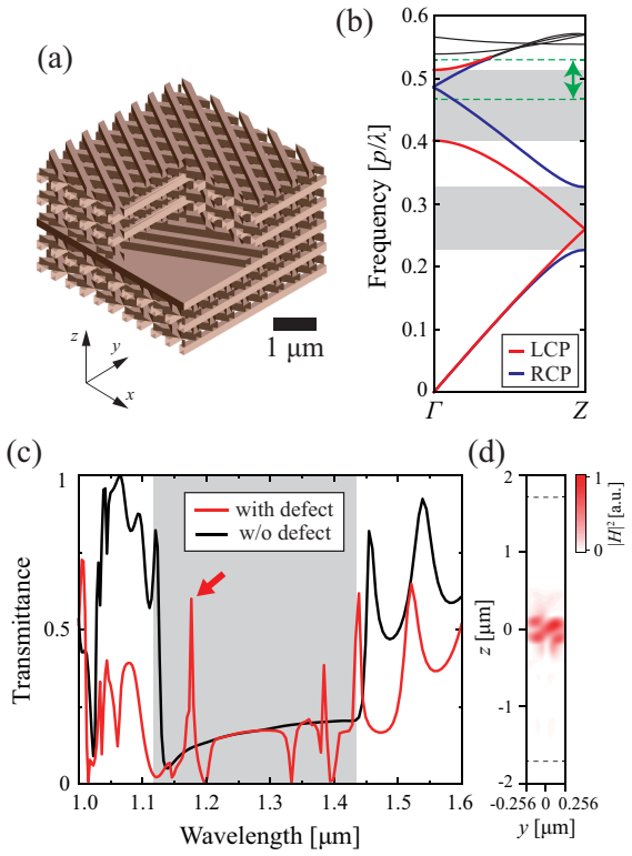
The central object is a chiral woodpile photonic crystal: stacked GaAs plates with rod patterns rotated by 120 degrees per plate, three plates forming a helical pitch of 570 nm, with a planar defect of 380 nm thickness inserted at the center. The helical stacking produces a photonic band structure with polarization-dependent bands and two polarization bandgaps, one suppressing left-handed circular polarization in the measured wavelength range. Inserting the planar defect creates cavity modes localized around the defect. The measured quantity is the degree of circular polarization, defined as the normalized difference between the left- and right-handed emission intensities; its wavelength, position, and temperature dependence are used to identify the cavity-mode peak.
What would settle it
Measure the circular-polarization-resolved photoluminescence of a bare InAs quantum-dot ensemble without the photonic crystal, at the same temperature, excitation power, and wavelength range; if the bare dots already show a positive degree-of-circular-polarization feature near 1160 nm, the observed cavity-mode peak could come from the emitters rather than from the chiral photonic environment. Alternatively, time-resolve the luminescence from quantum dots in the defect: if the left-handed component of the 1160 nm mode does not decay faster than the right-handed background, the claimed local density-of-states enhancement is not present.
Extended reading notes
Core claim
The central claim is that inserting a planar defect into a semiconductor three-dimensional chiral photonic crystal creates a cavity mode whose optical density of states is enhanced for left-handed circularly polarized light, even though the surrounding polarization bandgap suppresses that handedness. Embedded InAs quantum dots emit preferentially right-handed light across the bandgap, but at 1160 nm a distinct left-handed cavity-mode peak appears with a degree of circular polarization of +0.1 and a quality factor of about 390. The positive sign at the cavity mode, rather than the zero value expected from a passive circular-polarization bandpass filter, indicates a genuine enhancement of the left-handed vacuum-field density of states at the defect. Numerical transmission and radiative-rate calculations place the cavity mode at a nearby wavelength and reproduce the suppression of left-handed emission elsewhere in the bandgap.
Load-bearing premise
The measurement assumes the bare InAs quantum-dot ensemble emits with a wavelength-independent circular polarization, so any structure in the degree-of-circular-polarization spectrum is produced by the photonic environment; if the dots themselves emit a wavelength-dependent circular polarization near 1160 nm, the cavity-mode assignment loses its basis.
Editorial extensions
If this is right
- A semiconductor chip can produce circularly polarized light without a magnetic field or spin-polarized carriers, because the chiral cavity vacuum field itself selects the handedness.
- The planar-defect geometry provides a large two-dimensional gain region, which is a plausible route toward circularly polarized micro-lasing.
- At telecommunications wavelengths, a left-handed cavity mode coupled to quantum-dot emission could serve as a spin-photon interface for quantum communication.
- Chiral cavities of this kind could be combined with molecular emitters to move toward molecular chiral polaritons in the strong-coupling regime.
- The measured suppression of left-handed emission across the bandgap and its enhancement at the defect confirms that the photonic environment controls the local circular-polarization density of states.
Reading between the lines
- A direct test the paper does not report is polarization-resolved photoluminescence of the bare InAs quantum-dot ensemble without the photonic crystal over the same wavelength and temperature range; this would isolate any intrinsic wavelength-dependent circular polarization in the emitters themselves.
- The degree of circular polarization at the cavity mode is small, so practical spin-photon interfaces would require systematic control of emitter-cavity detuning and quantum-dot dipole orientation, which the paper leaves open.
- In the second tested cavity, the degree of circular polarization at the cavity peak remains negative, suggesting the sign of the peak may depend on the relative spectral position of the quantum-dot ensemble and the cavity mode; a detuning series would separate genuine density-of-states enhancement from wavelength-dependent filtering.
Editorial analysis
A structured set of objections, weighed in public.
Referee Report
Summary. Takahashi et al. report low-temperature photoluminescence measurements of InAs quantum dots embedded in a planar defect inside a GaAs-based chiral woodpile photonic crystal. They observe a spectrally broad negative degree of circular polarization, which they attribute to a left-handed polarization bandgap, and a spatially localized positive DOP peak at about 1160 nm, which they identify as a left-handed circularly polarized cavity mode with Q~390. Supporting evidence includes the temperature shift of the peak (0.05 nm/K versus 0.14 nm/K for bare QDs), a second sample in Appendix B, and FDTD calculations of transmission and of the spontaneous-emission modification for LCP and RCP sources. The paper concludes that the chiral photonic environment enhances the LCP local density of states at the cavity mode.
Significance. If the central claim holds, this is a notable advance: it demonstrates a semiconductor-based three-dimensional chiral photonic-crystal cavity with circular-polarization-selective Purcell enhancement, with potential applications in compact circularly polarized light sources, spin-photon interfaces, and chiral polaritonics. The manuscript has real strengths: the FDTD transmission and spontaneous-emission calculations are independent predictions made from design parameters rather than fits to the measured DOP; the spatial-localization and temperature-shift measurements are appropriate tests of the cavity-mode assignment; and the second-sample result in Appendix B provides partial reproducibility. The main weaknesses are an apparent internal inconsistency in the reported lifetime-ratio result and the absence of a direct control on the intrinsic circular polarization of the quantum-dot ensemble; both need to be addressed before the claim is fully supported.
major comments (2)
- [Main text (paragraph after Fig. 3) and Appendix C, Fig. 6(b)] The numerical support for the positive DOP peak is internally inconsistent as written. The main text states that the FDTD calculations show 'the LCP radiative rates are larger than those for RCP around the cavity wavelength,' but Appendix C reports a 'broad peak of τLCP/τRCP > 1 around a wavelength of 1170 nm' in the 'lifetime ratio.' Because a longer lifetime corresponds to a smaller radiative rate, τLCP/τRCP > 1 implies that RCP, not LCP, has the faster emission, which would predict a negative DOP at the cavity mode, opposite to the measured +0.1 peak. The statement that τLCP/τRCP < 1 around 1120 nm and 1210 nm is 'consistent with the LCP polarization band gap' is likewise only true if the plotted quantity is a rate ratio ΓLCP/ΓRCP rather than a lifetime ratio. Please clarify whether the plotted quantity is a lifetime ratio or a rate ratio; if it is a lifetime, the calculation as presented does not confirm the claimed enhancement of the LCP density of states. This point is load-bearing because this calculation is cited as direct confirmation of the cavity-mode interpretation.
- [Appendix A and PL measurements (Fig. 3)] The attribution of the positive DOP peak to chiral-cavity Purcell enhancement assumes that the InAs quantum-dot ensemble in the unpatterned active plates has no intrinsic wavelength-dependent circular polarization. Appendix A characterizes the bare QDs only through unpolarized intensity spectra and through the temperature shift of one bright QD at 1052 nm; it does not provide a DOP spectrum of the active plates, or of QDs outside the photonic crystal, in the 1100-1250 nm range. Because local strain, size distributions, or anisotropic exchange splitting can produce nonzero ensemble DOP, a direct DOP control measured under identical excitation and detection conditions would materially strengthen the assignment of the +0.1 peak to the photonic environment rather than to the emitters themselves. As written, the alternative explanation that the positive DOP arises partly or wholly from the QD ensemble is not fully excluded.
minor comments (5)
- [Main text and Fig. 3(c) caption] The main text reports the cavity-mode peak at 1160 nm, whereas the Fig. 3(c) caption states a peak at 1165 nm; please harmonize these values.
- [Appendix A] The bare-QD temperature shift is measured for a single bright QD at 1052 nm over 44-58 K, whereas the cavity DOP peak is near 1160 nm and the temperature dependence is measured over 60-80 K. The comparison implies that all QD ensemble transitions shift at the same rate over the same range; this assumption should be stated explicitly or tested for the ensemble at the relevant wavelength.
- [Fig. 3(d)] The position-dependence data would benefit from error bars and a quantitative linewidth of the spatial localization profile; as presented, the spatial extent of the DOP peak cannot be judged beyond the qualitative decrease with displacement.
- [Appendix C, Fig. 6(b)] The lifetime-ratio plot lacks error bars from the six source positions despite the text stating that the modification coefficients are averaged over the six simulations; reporting the standard error or range would help assess the significance of the peak above unity.
- [Appendix C, sentence near Fig. 6] The text contains a typo, 'a braod peak,' which should read 'a broad peak.'
Circularity Check
No significant circularity: the central claim is supported by independent FDTD calculations and control measurements, not by fitted inputs or self-citations.
full rationale
The paper's derivation chain is an experimental observation (the DOP spectrum in Fig. 3(b,c)) cross-checked against several independent numerical and control results: a plane-wave band-structure calculation of the polarization bandgap (Fig. 1(b)), an FDTD transmission calculation using design parameters that yields a cavity mode at 1176 nm with Q ~ 1167 (Fig. 1(c,d)), a position-dependence measurement localizing the DOP peak to the structure (Fig. 3(d)), a temperature-shift comparison with bare QD emission measured in Appendix A, and an FDTD lifetime-ratio calculation giving tau_LCP/tau_RCP > 1 near the cavity wavelength (Appendix C). None of these numerical results is fitted to the measured DOP; the structural parameters are specified from the design, and the discrepancy between measured Q ~ 390 and calculated Q ~ 1167 is explicitly acknowledged as a fabrication-error effect. Self-citations (Refs. 9, 18-24) provide prior context and fabrication methods, but every load-bearing quantitative check is either recomputed in this paper or measured directly, so the argument does not reduce to its own inputs. The strongest remaining caveat is that the circular polarization of bare QD emission is not directly measured, which leaves the unpolarized-emitter assumption unverified; that is a correctness concern, not a circular derivation.
Assumptions & free parameters
free parameters (2)
- Planar defect thickness =
380 nm (design); 400 nm in second cavity
- Rod width, period, and plate thickness =
150 nm / 450 nm / 190 nm
assumptions (4)
- domain assumption Plane-wave expansion and FDTD methods correctly model the fabricated dielectric structure with a constant refractive index of 3.4 for GaAs.
- domain assumption The ensemble of InAs quantum dots in the planar defect emits unpolarized, broadband light in the absence of a magnetic field.
- domain assumption The fabricated 16-plate stack with approximately 50 nm stacking error faithfully realizes the simulated chiral lattice and planar defect.
- domain assumption The two unpatterned active plates act as a planar defect with effective refractive index 3.4 and thickness equal to two 190 nm plates.
Cite this review
Pith. "Pith review of Circularly polarized cavity-mode emission from quantum dots in a semiconductor three-dimensional chiral photonic crystal." pith.science (2026). https://pith.science/paper/2PJT6DJO
@misc{pith2026241118098,
  author       = {Pith},
  title        = {Pith review of: Circularly polarized cavity-mode emission from quantum dots in a semiconductor three-dimensional chiral photonic crystal},
  year         = {2026},
  howpublished = {\url{https://pith.science/paper/2PJT6DJO}},
  note         = {Machine review of arXiv:2411.18098}
}
read the original abstract
We experimentally demonstrated a circularly polarized cavity mode in a GaAs-based chiral photonic crystal (PhC) containing a planar defect. Low-temperature photoluminescence measurements of InAs quantum dots (QDs) embedded in the planar defect revealed a polarization bandgap for left-handed circularly polarized light in the near-infrared spectrum. Within this bandgap, where the QDs preferably emitted right-handed circularly polarized light, we observed a distinct cavity-mode peak characterized by left-handed circular polarization. This observation indicates that the chiral PhC modifies the optical density of states for left-handed circular polarization to be suppressed in the polarization bandgap and be largely enhanced at the cavity mode. The results obtained may not only provide photonic devices such as compact circularly polarized light sources but also promote strong coupling between circularly polarized photons and excitons in solid states or molecules, paving the way for advancements in polaritonics, spintronics, and quantum information technology.
Figures


Figures from the paper (3 more)


Reference graph
Works this paper leans on
-
[1]
F. Meier and B. P. Zakharchenya, Optical Orientation (North-Holland, Amsterdam, 2012)
work page 2012
-
[2]
H. Ando, T. Sogawa, and H. Gotoh, ``Photon-spin controlled lasing oscillation in surface-emitting lasers,'' Appl. Phys. Lett. 73 , 566 (1998)
work page 1998
-
[3]
S. Iba, S. Koh, K. Ikeda, and H. Kawaguchi, ``Room temperature circularly polarized lasing in an optically spin injected vertical-cavity surface-emitting laser with (110) GaAs quantum wells,'' Appl. Phys. Lett. 98 , 081113 (2011)
work page 2011
-
[4]
K. D. Greve, L. Yu, P. L. McMahon, J. S. Pelc, C. M. Natarajan, N. Y. Kim, E. Abe, S. Maier, C. Schneider, M. Kamp, S. Hofling, R. H. Hadfield, A. Forchel, M. M. Fejer, and Y. Yamamoto, ``Quantum-dot spin-photon entanglement via frequency downconversion to telecom wavelength,'' Nature 491, 421--425 (2012)
work page 2012
-
[5]
W. B. Gao, P. Fallahi, E. Togan, J. M. Sanchez, and A. Imamoglu, ``Observation of entanglement between a quantum dot spin and a single photon,'' Nature 491, 426--429 (2012)
work page 2012
-
[6]
A. A. Demenev, V. D. Kulakovskii, C. Schneider, S. Brodbeck, M. Kamp, S. H o fling, S. V. Lobanov, T. Weiss, N. A. Gippius, and S. G. Tikhodeev, ``Circularly polarized lasing in chiral modulated semiconductor microcavity with GaAs quantum wells,'' Appl. Phys. Lett. 109 , 171106 (2016)
work page 2016
-
[7]
J. K. Gansel, M. Thiel, M. S. Rill, M. Decker, K. Bade, V. Saile, G. von Freymann, S. Linden, and M. Wegener, ``Gold helix photonic metamaterial as braodband circular polarizer,'' Science 325, 1513--1515 (2009)
work page 2009
-
[8]
J. C. W. Lee and C. T. Chan, ``Polarization gaps in spiral photonic crystals,'' Optics Express 13, 8083--8088 (2005)
work page 2005
Show all 27 references
-
[9]
Takahashi, T
S. Takahashi, T. Tajiri, Y. Arakawa, S. Iwamoto, and W. L. Vos, ``Optical properties of chiral three-dimensional photonic crystals,'' Phys, Rev, B 107 , 165307 (2023)
2023
-
[10]
J. D. Joannopoulos, S. G. Johnson, J. N. Winn, and R. D. Meade, Photonic Crystals: Molding the Flow of Light, 2nd ed. (Princeton University Press, Princeton NJ, 2008)
2008
-
[11]
Sakoda, Optical Properties of Photonic Crystals, 2nd ed
K. Sakoda, Optical Properties of Photonic Crystals, 2nd ed. (Springer, New York, 2005)
2005
-
[12]
V. I. Kopp, Z.-Q. Zhang, and A. Z. Genack, ``Lasing in chiral photonic structures,'' Prog. Quantum Electron. 27, 369--416 (2003)
2003
-
[13]
Schmidtke, W
J. Schmidtke, W. Stille, and H. Finkelmann, ``Defect Mode Emission of a Dye Doped Cholesteric Polymer Network,'' Phys. Rev. Lett. 90, 083902 (2003)
2003
-
[14]
M. H. Song, N. Y. Ha, K. Amemiya, B. Park, Y. Takanishi, K. Ishikawa, J. W. Wu, S. Nishimura, T. Toyooka, H. Takezoe, ``Defect-Mode Lasing with Lowered Threshold in a Three-Layered Hetero-Cholesteric Liquid-Crystal Structure,'' Adv. Matter. 18, 193--197 (2006)
2006
-
[15]
S. M. Jeong, N. Y. Ha, Y. Takanishi, K. Ishikawa, H. Takezoe, S. Nishimura, and G. Suzaki, ``Defect mode lasing from a double-layered dye-doped polymeric cholesteric liquid crystal films with a thin rubbed defect layer,'' Appl. Phys. Lett. 90 , 261108 (2007)
2007
-
[16]
Fujita, K
T. Fujita, K. Morimoto, H. Kiyama, G. Allison, M. Larsson, A. Ludwig, S. R. Valentin, A. D. Wieck, A. Oiwa, and S. Tarucha, ``Angular momentum transfer from photon polarization to an electron spin in a gate-defined quantum dot,'' Nat. Commun. 10, 2991 (2019)
2019
-
[17]
D. G. Baranov, C. Sch a fer, and M. V. Gorkunov, ``Toward Molecular Chiral Polaritons,'' ACS Photonics 10, 2440--2455 (2023)
2023
-
[18]
Takahashi, T
S. Takahashi, T. Tajiri, Y. Ota, J. Tatebayashi, S. Iwamoto, and Y. Arakawa, Appl. Phys. Lett. 105 , 051107 (2014)
2014
-
[19]
Takahashi, E
S. Takahashi, E. Kimura, T. Ishida, T. Tajiri, K. Watanabe, K. Yamashita, S. Iwamoto, and Y. Arakawa, ``Fabrication of three-dimensional photonic crystals for near-infrared light by micro-manipulation technique under optical microscope observation,'' Appl. Phys. Express 15 , 0...
2021
-
[20]
K. Aoki, D. Guimard, M. Nishioka, M. Nomura, S. Iwamoto, and Y. Arakawa, ``Coupling of quantum-dot light emission with a three-dimensional photonic-crystal nanocavity,'' Nat. Photonics 2, 688--692 (2008)
2008
-
[21]
Tandaechanurat, S
A. Tandaechanurat, S. Ishida, D. Guimard, M. Nomura, S. Iwamoto, and Y. Arakawa, ``Lasing oscillation in a three-dimensional photonic crystal nanocavity with a complete bandgap,'' Nat. Photonics 5, 91--94 (2010)
2010
-
[22]
Takahashi, T
S. Takahashi, T. Tajiri, K. Watanabe, Y. Ota, S. Iwamoto, and Y. Arakawa, ``High-Q nanocavities in semiconductor-based three-dimensional photonic crystals,'' Electron. Lett. 54 , 305 (2018)
2018
-
[23]
Konishi, M
K. Konishi, M. Nomura, N. Kumagai, S. Iwamoto, Y. Arakawa, and M. K.-Gonokami, ``Circularly polarized light emission from semiconductor planar chiral nanostructures,'' Phys. Rev. Lett. 106, 057402 (2011)
2011
-
[24]
Takahashi, Y
S. Takahashi, Y. Ota, T. Tajiri, J. Tatebayashi, S. Iwamoto, and Y. Arakawa, ``Circularly polarized vacuum field in three-dimensional chiral photonic crystals probed by quantum dot emission,'' Phys. Rev. B 96 , 195404 (2017)
2017
-
[25]
Tandaechanurat, S
A. Tandaechanurat, S. Ishida, K. Aoki, D. Guimard, M. Nomura, S. Iwamoto, and Y. Arakawa, ``Demonstration of high- Q ( > 8600) three-dimensional photonic crystal nanocavity embedding quantum dots,'' Appl. Phys. Lett. 94 , 171115 (2009)
2009
-
[26]
Tajiri, S
T. Tajiri, S. Takahashi, Y. Ota, J. Tatebayashi, S. Iwamoto, and Y. Arakawa, ``Demonstration of a three-dimensional photonic crystal nanocavity in a < 110 > -layered diamond structure,'' Appl. Phys. Lett. 107 , 071102 (2015)
2015
-
[27]
Xu, et al
Y. Xu, et al. , J. Opt. Soc. Am. B 16 , 465 (1999)
1999
Reviewed August 12, 2026 · model on record in the stance chip above.
Discussion (0). Continue with ORCID to comment.