REVIEW 3 major objections 5 minor 31 references
Simulation of irradiated hybrid planar pixels modules at fluences expected at HL-LHC
T0 review · 3 major / 5 minor · reviewed 2026-08-07 · deepseek-v4-flash
Pith's one-line read Combined TCAD and Monte Carlo simulations predict ATLAS ITk planar pixel modules will collect enough charge at HL-LHC fluences to maintain full hit efficiency.
desk verdict A probing but single-point validation of a TCAD/Allpix2 chain; the ITk 'full efficiency' claim outruns the evidence. read the letter →
The pith
A machine-rendered reading of the paper's core claim, the machinery that carries it, and where it could break.
The reading
What carries the argument
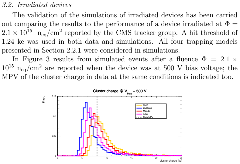
The load-bearing object is a two-stage simulation chain. Silvaco TCAD produces 3D maps of the electric field and weighting potential for a 50x50 µm2 n-on-p pixel cell, using the LHCb VELO radiation damage model to describe defect states created by irradiation. Allpix2 v3.2.0 then transports charge from 120 GeV pions impinging at normal incidence, applying a mobility model, digitization thresholds, and a carrier-trapping model. The chosen trapping model is the average of the CMS and Mandić parameterizations, whose predictions bracket the measured data; the semi-difference of the two is assigned as the systematic uncertainty.
What would settle it
Measure the cluster charge MPV of an ATLAS ITkPixV2 planar module (100 µm or 150 µm thick) irradiated to 3.5e15 neq/cm2 and biased at 400 V. If the measured MPV is below the effective threshold of about 1.3 ke, or deviates by more than the predicted uncertainty band from the simulated 5 ke (thin) or 6 ke (thick), the transferability of the validated models to the full ITk fluence range is ruled out.
Extended reading notes
Core claim
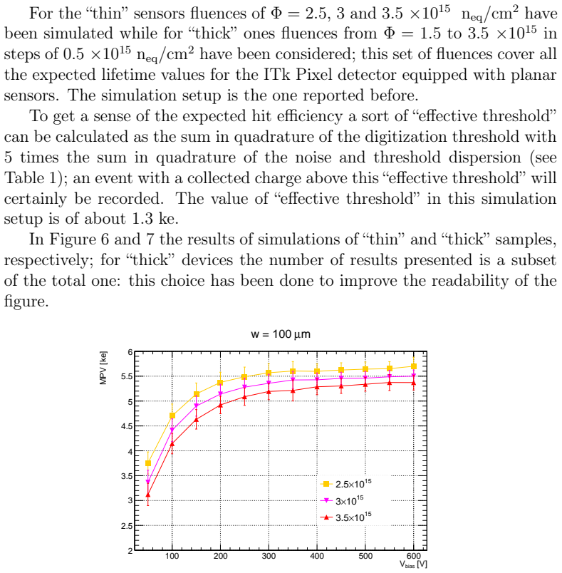
The central claim is that, at all fluences and voltages simulated and for both sensor thicknesses, enough charge is collected to have full efficiency for normally incident particles: for thin sensors the predicted most probable charge is above 5 ke at 400 V even at the largest fluence of 3.5e15 neq/cm2, and for thick sensors it is always above 6 ke. This follows from the validation step, where the combination of the LHCb radiation damage model (two deep acceptors, one donor) in TCAD and the average of the CMS and Mandić trapping models matches the measured cluster charge as a function of bias voltage for an irradiated 150 µm sensor, correctly predicting the voltage at which saturation begins. Consequently, the paper states that it will not be necessary to operate the ITk pixel modules at the maximum 600 V bias.
Load-bearing premise
The validation is performed at one fluence (2.1e15 neq/cm2) on one sensor thickness (150 µm), and this single point is taken as sufficient to guarantee the LHCb radiation damage model and the averaged CMS–Mandić trapping model are accurate for 100 µm and 150 µm ATLAS ITk planar sensors at fluences from 1.5 to 3.5e15 neq/cm2.
Editorial extensions
If this is right
- ATLAS ITk planar pixel modules can be operated at 300–400 V bias instead of the maximum 600 V, reducing power draw and easing the cooling budget.
- The validated chain can produce radiation-damage look-up tables for the ATLAS Monte Carlo generator, allowing tracking and vertexing algorithms to be tested under realistic HL-LHC charge-collection conditions.
- Even after 40% or more signal loss, the collected charge is predicted to remain several times above the effective threshold of about 1.3 ke, implying high hit efficiency throughout the detector lifetime.
- The same simulation setup can be extended to future sensor designs or readout chips once new irradiated test-beam data become available.
Reading between the lines
- The validation rests on a single fluence–thickness point; measuring a second point at 3.5e15 neq/cm2 on a 100 µm sensor would directly test whether the LHCb damage model and the averaged trapping model transfer across the full ITk fluence range.
- The simulations use particles at normal incidence, which suppresses charge sharing; real ATLAS tracks arrive at a range of angles, so per-pixel collected charge will be lower than simulated, and the 'full efficiency' claim is safest for cluster-level charge.
- The success of averaging two bracketing trapping models suggests a single unified trapping-rate parameterization covering 1e15 to 1e17 neq/cm2 could simplify future simulations.
- The same validated chain could be applied to 3D sensors, though the paper notes their different geometry and fluence range (up to 1.6e16 neq/cm2) require a dedicated study.
Editorial analysis
A structured set of objections, weighed in public.
Referee Report
Summary. The paper validates a combined TCAD (Silvaco) and Allpix2 Monte Carlo simulation chain for irradiated hybrid planar pixel sensors. Validation is performed against CMS passive CMOS n-on-p sensors (150 µm thick, 50×50 µm² pitch) irradiated to Φ = 2.1×10^15 neq/cm², comparing cluster-charge MPV versus bias voltage for four trapping models (CMS, Ljubljana, Atlas, Mandić). The authors find that the CMS and Mandić models bracket the data and adopt their average, with the semi-difference as uncertainty. They then apply this validated setup to predict the collected charge of ATLAS ITk planar sensors (100 µm and 150 µm thick) at fluences from 1.5×10^15 to 3.5×10^15 neq/cm², concluding that enough charge is collected for full efficiency at all considered fluences and voltages, and that operation at moderate bias voltages (well below 600 V) should be possible.
Significance. If the predictions are correct, the paper would provide valuable guidance for operating the ATLAS ITk pixel detector at HL-LHC fluences and for preparing radiation-damage-aware Monte Carlo simulations. The manuscript has genuine strengths: the unirradiated simulation reproduces the data MPV within 1% (Section 3.1); the voltage dependence of the collected charge in the irradiated case is reproduced by all four trapping models, which independently supports the TCAD electric-field modelling; and the trapping-model parameters are taken from external, published fits rather than fitted to the validation data. However, the central extrapolation to ITk sensors rests on a single validation point, and the adopted uncertainty band is constructed post hoc. These issues currently limit the strength of the conclusions.
major comments (3)
- [Section 3.2 and Section 4] The validation is performed on a single sensor (150 µm thick, n-on-p passive CMOS, Φ = 2.1×10^15 neq/cm²), and this single point is used to justify extrapolation in Section 4 to 100 µm thick "thin" ITk sensors and to fluences up to 3.5×10^15 neq/cm². This is a two-directional extrapolation in both thickness and fluence, and no independent data are used to test either direction. Reference [16] reports measurements at other fluences, including up to 1×10^16 neq/cm², and the paper itself notes these data in Section 2.2.1, but they are not used for validation. The claim in Section 4 that "at all fluences and voltages and for both thicknesses enough charge is collected to have full efficiency" is therefore not supported by the evidence presented.
- [Section 4] The averaging of the CMS and Mandić trapping models, with the uncertainty taken as their semi-difference, is decided after inspecting the data at one fluence and one thickness. This makes the uncertainty band a post hoc envelope rather than a predictive uncertainty. The two models have different functional forms (linear in Φ for CMS, power-law for Mandić), so their difference at Φ = 2.1×10^15 neq/cm² does not guarantee that they will bracket the true collected charge at Φ = 3.5×10^15 neq/cm² or for 100 µm sensors. The fluence-dependence of the uncertainty band in Figures 6–9 is therefore not justified and should be either validated against additional data or presented as an assumption.
- [Section 4] The statement "At all fluences and voltages and for both thicknesses enough charge is collected to have full efficiency" is based on comparing the simulated MPV of the cluster charge to an "effective threshold" of about 1.3 ke, not on a simulated hit efficiency. The simulation uses 120 GeV pions at normal incidence with essentially no charge sharing, which is an optimistic scenario. For inclined tracks, clusters with more charge sharing, or with the actual readout threshold and cluster algorithm, the hit efficiency could be lower even if the MPV exceeds the threshold by a wide margin. The paper should either compute a realistic hit efficiency or qualify the "full efficiency" claim to say that the collected charge is expected to be well above threshold under the idealized conditions simulated.
minor comments (5)
- [Section 2.2 and Section 3.2] Table 1 lists a digitization threshold of 600 e, whereas Section 3.2 states that "a hit threshold of 1.24 ke was used in both data and simulations." Please clarify which threshold applies to the validation and which to the ITk predictions, and whether the difference is intentional.
- [Section 3.2] The sentence "It is interesting to notice that the Mandić and CMS trapping models essentially bracket the data in the 'depleted' region" is followed by a statement that Mandić is closer to data, but then the average is adopted. The rationale for preferring the average over the single better-performing Mandić model is not fully articulated; please spell out the reasoning.
- [Section 4] The definition of the "effective threshold" as the quadratic sum of the threshold with 5 times the quadratic sum of noise and threshold dispersion should be justified; the factor of 5 appears arbitrary and is not motivated in the text.
- [Figure 8] The vertical axis label in Figure 8 reads "MIP [ke-]", which is inconsistent with all other figures that use "MPV [ke]"; please correct.
- [Section 3.1] There is a typographical spacing error in "CMStrackergroupreported" near the end of Section 3.1; the text should read "CMS tracker group reported".
Circularity Check
No significant circularity: model parameters are external fits, and the HL-LHC predictions are extrapolations of a fixed simulation, not outputs fitted to the target data.
full rationale
The paper's derivation chain is not circular. The TCAD radiation damage model is the external LHCb VELO model (ref [27]), and the four trapping models tested (CMS, Ljubljana, Atlas, Mandić) are independent published parameterizations fitted to their own datasets (refs [11], [29], [4], [30]). The validation at Φ = 2.1×10^15 neq/cm² compares these fixed models to test-beam data; the 'combination' used for final predictions is an equal-weight average of the CMS and Mandić models with the semi-difference as an uncertainty band. That averaging is a post-hoc model-selection choice informed by the validation data, but no equation in the paper determines the predicted MPV from the validation data by construction, and the model parameters are not fitted to the CMS passive-CMOS measurements. The Section 4 predictions for 100 µm and 150 µm ATLAS ITk sensors at other fluences are genuine extrapolations of the fixed averaged model; they are not statistically forced by the single validation point. Self-citations appear (refs [6] and [13]), but neither is load-bearing: [6] supports an introductory statement about existing ATLAS digitizer algorithms, and [13] is named as a future consumer of lookup tables rather than an input to the validation or prediction. The paper itself honestly notes that no ITkPixV2 modules exist yet and that similar data on passive CMOS sensors are used as a proxy. The main weakness, namely single-point validation and transferability to other fluences and to ITk planar technology, is an extrapolation risk and not a circular reduction. Accordingly, no circular step can be exhibited under the strict standard of quoting an equation or a fitted-input-called-prediction reduction.
Assumptions & free parameters
free parameters (6)
- CMS trapping model coefficients beta_e,h and tau0_e,h =
beta_e=1.7e16 cm2/ns, beta_h=2.8e16 cm2/ns, tau0_e=0.11/ns, tau0_h=0.09/ns
- Mandic trapping model coefficients c and kappa =
c=0.54 ns, kappa=-0.62
- Atlas trapping model coefficients =
beta_e=4.5e16 cm2/ns, beta_h=6.5e16 cm2/ns
- Ljubljana trapping model coefficients =
beta_e(T0)=5.6e16 cm2/ns, beta_h(T0)=7.7e16 cm2/ns, kappa_e=-0.86, kappa_h=-1.52
- CMS and Mandic average weights =
0.5/0.5
- Effective threshold factor =
5 sigma
assumptions (5)
- domain assumption The LHCb radiation damage model [27] with two deep acceptor states and one donor state correctly describes the electric field in irradiated n-on-p sensors at fluences up to 3.5e15 neq/cm2.
- domain assumption The CMS passive CMOS RD53A data at 2.1e15 neq/cm2 [15,16] are representative of ATLAS ITk planar pixel modules for the purpose of model validation.
- domain assumption Trapping model parameters from the literature (CMS, Mandic, Atlas, Ljubljana) apply directly to the simulated 150 micrometer and 100 micrometer n-on-p 50x50 micrometer sensors.
- domain assumption The average free path of carriers remains larger than the sensor thickness at the considered fluences, so thicker sensors collect more charge.
- domain assumption Normal-incidence 120 GeV pion beam approximates the particle environment for efficiency conclusions.
Cite this review
Pith. "Pith review of Simulation of irradiated hybrid planar pixels modules at fluences expected at HL-LHC." pith.science (2026). https://pith.science/paper/KYUB6RTI
@misc{pith2026250610823,
  author       = {Pith},
  title        = {Pith review of: Simulation of irradiated hybrid planar pixels modules at fluences expected at HL-LHC},
  year         = {2026},
  howpublished = {\url{https://pith.science/paper/KYUB6RTI}},
  note         = {Machine review of arXiv:2506.10823}
}
read the original abstract
Signal loss is the main limitation on tracking/vertexing performance due to radiation damage effect to hybrid pixel detectors when irradiated at fluences expected at High Luminosity LHC (HL-LHC). It is important to have reliable predictions on the charge collection performance after irradiation in order to predict operational voltage values and test tracking algorithms robustness. In this paper the validation of combined TCAD and Monte Carlo simulations of hybrid silicon planar pixels sensors will be presented. In particular different trapping models will be compared to identify the one giving the best predictions. Eventually predictions on the collected charge performance of planar pixels modules at HL-LHC will be discussed.
Figures


Figures from the paper (6 more)




Reference graph
Works this paper leans on
-
[16]
Glessgen, Characterization of irradiated passive cmos sensors for tracking in hep experiments, Nucl
F. Glessgen, Characterization of irradiated passive cmos sensors for tracking in hep experiments, Nucl. Instr. and Meth. A 1046 (2023) 167694. doi:https://doi.org/10.1016/j.nima.2022.167694. URL https://www.sciencedirect.com/science/article/pii/S016890022200986X
-
[1]
I. Dawson, Radiation effects in the LHC experiments: Impact on detec- tor performance and operation, CERN Yellow Reports: Monographs, CERN, Geneva, 2021. doi:10.23731/CYRM-2021-001. URL https://cds.cern.ch/record/2764325
-
[2]
M. Moll, Displacement damage in silicon detectors for high energy physics, IEEE Transactions on Nuclear Science 65 (8) (2018) 1561–1582. doi:10.1109/TNS.2018.2819506
-
[3]
Performance of ATLAS Pixel Detector and Track Reconstruction at the start of Run 3 in LHC Collisions at√s = 900 GeV, Tech. rep., CERN, 14 Geneva (2022). URL https://cds.cern.ch/record/2814766
arXiv 2022
-
[4]
M. Aaboud, et al., Modelling radiation damage to pixel sensors in the ATLAS detector, JINST 14 (06) (2019) P06012–P06012. doi:10.1088/1748-0221/14/06/p06012
-
[5]
M. Swartz, D. Fehling, G. Giurgiu, P. Maksimovic, V. Chiochia, A new technique for the reconstruction, validation, and simulation of hits in the CMS Pixel Detector, PoS Vertex 2007 (2008) 035. doi:10.22323/1.057.0035
-
[6]
Marco Bomben, on behalf of the ATLAS Collaboration, Including ra- diation damage effects in ATLAS Monte Carlo simulations: status and perspectives, in: Proceedings of The European Physical Society Confer- ence on High Energy Physics — PoS(EPS-HEP2023), Vol. 449, 2024, p
work page 2024
-
[7]
URL https://hilumilhc.web.cern.ch/content/hl-lhc-project
The HL-LHC project. URL https://hilumilhc.web.cern.ch/content/hl-lhc-project
Show all 31 references
-
[8]
ATLAS Collaboration, Technical Design Report for the ATLAS Inner Tracker Pixel Detector, Tech. Rep. CERN-LHCC-2017-021. ATLAS- TDR-030, CERN, Geneva (Sep 2017). URL https://cds.cern.ch/record/2285585
2017
-
[9]
URL https://cds.cern.ch/record/2257755
Technical Design Report for the ATLAS Inner Tracker Strip Detector (Apr 2017). URL https://cds.cern.ch/record/2257755
2017
-
[10]
doi:10.1088/1748-0221/20/02/P02018
The ATLAS collaboration, Expected tracking performance of the AT- LAS Inner Tracker at the High-Luminosity LHC, Journal of Instrumen- tation 20 (02) (2025) P02018. doi:10.1088/1748-0221/20/02/P02018. URL https://dx.doi.org/10.1088/1748-0221/20/02/P02018
2025 doi
-
[11]
Spannagel, K
S. Spannagel, K. Wolters, D. Hynds, N. Alipour Tehrani, M. Benoit, D. Dannheim, N. Gauvin, A. NÃŒrnberg, P. SchÃŒtze, M. Vi- cente, Allpix2: A modular simulation framework for silicon detectors, Nucl. Instrum. and Meth. A 901 (2018) 164–172. doi:https://doi.org/10.1016/j.nima....
2018 doi
-
[12]
Hakan Wennlof and Dominik Dannheim and Manuel Del Rio Viera and others, Simulating monolithic active pixel sen- sors: A technology-independent approach using generic dop- ing profiles, Nucl. Instr. and Meth. A 1073 (2025) 170227. doi:https://doi.org/10.1016/j.nima.2025.170227....
2025
-
[13]
Nakkalil, M
K. Nakkalil, M. Bomben, A lightweight algorithm to model radiation damage effects in monte carlo events for high-luminosity large hadron collider experiments, Sensors 24 (12) (2024). doi:10.3390/s24123976. URL https://www.mdpi.com/1424-8220/24/12/3976
2024 doi
-
[14]
L. L. Pottier, T. Heim, M. Garcia-Sciveres, Testing the limits of itkpixv2: the atlas inner tracker pixel detector readout chip (2025). arXiv:2502.05097. URL https://arxiv.org/abs/2502.05097
2025 arXiv
-
[15]
Glessgen, M
F. Glessgen, M. Backhaus, F. Canelli, Y. M. Dieter, J. C. Dingfelder, T. Hemperek, F. Huegging, A. Jofrehei, W. Jin, B. Kilminster, A. Mac- chiolo, D. Muenstermann, D.-L. Pohl, B. Ristic, R. Wallny, T. Wang, N. Wermes, P. Wolf, Characterization of passive cmos sensors with rd5...
2022 doi
-
[17]
Garcia-Sciveres, The RD53A Integrated Circuit, Tech
M. Garcia-Sciveres, The RD53A Integrated Circuit, Tech. rep., CERN, Geneva (2017). URL https://cds.cern.ch/record/2287593
2017
-
[19]
Allison, et al., Geant4 developments and applications, IEEE Transactions on Nuclear Science 53 (1) (2006) 270–278
J. Allison, et al., Geant4 developments and applications, IEEE Transactions on Nuclear Science 53 (1) (2006) 270–278. doi:10.1109/TNS.2006.869826
2006
-
[20]
Allison, et al., Recent developments in geant4, Nucl
J. Allison, et al., Recent developments in geant4, Nucl. Instr. and Meth. A 835 (2016) 186–225. doi:https://doi.org/10.1016/j.nima.2016.06.125. URL https://www.sciencedirect.com/science/article/pii/S0168900216306957
2016 doi
-
[21]
Shockley, Currents to Conductors Induced by a Moving Point Charge, Journal of Applied Physics 9 (1938) 635
W. Shockley, Currents to Conductors Induced by a Moving Point Charge, Journal of Applied Physics 9 (1938) 635
1938
-
[22]
Ramo, Currents Induced by Electron Motion, Proceedings of the IRE 27 (1939) 584–585
S. Ramo, Currents Induced by Electron Motion, Proceedings of the IRE 27 (1939) 584–585. doi:10.1109/JRPROC.1939.228757
1939
-
[23]
Hurkx, D
G. Hurkx, D. Klaassen, M. Knuvers, A new recombination model for device simulation including tunneling, IEEE Transactions on Electron Devices 39 (2) (1992) 331–338. doi:10.1109/16.121690
1992 doi
-
[24]
Canali, G
C. Canali, G. Majni, R. Minder, G. Ottaviani, Electron and hole drift velocity measurements in silicon and their empirical relation to electric field and temperature, IEEE Transactions on Electron Devices 22 (11) (1975) 1045 – 1047. doi:https://doi.org/10.1109/T-ED.1975.18267
1975
-
[26]
Van Overstraeten, H
R. Van Overstraeten, H. De Man, Measurement of the ionization rates in diffused silicon p-n junctions, Solid-State Electronics 13 (5) (1970) 583–608. doi:https://doi.org/10.1016/0038-1101(70)90139-5. URL https://www.sciencedirect.com/science/article/pii/0038110170901395
1970
-
[27]
Folkestad and others, Development of a silicon bulk radiation damage model for sentaurus tcad, Nucl
Å. Folkestad and others, Development of a silicon bulk radiation damage model for sentaurus tcad, Nucl. Instrum. Meth. A874 (2017) 94 – 102. doi:https://doi.org/10.1016/j.nima.2017.08.042
2017 doi
-
[28]
Collaboration, LHCb VELO Upgrade Technical Design Report, Tech
L. Collaboration, LHCb VELO Upgrade Technical Design Report, Tech. Rep. CERN-LHCC-2013-021. LHCB-TDR-013 (Nov 2013). URL https://cds.cern.ch/record/1624070 17
2013
-
[29]
Kramberger, et al., Effective trapping time of electrons and holes in different silicon materials irradiated with neutrons, protons and pions, Nucl
G. Kramberger, et al., Effective trapping time of electrons and holes in different silicon materials irradiated with neutrons, protons and pions, Nucl. Instr. and Meth. A 481 (1-3) (2002) 297 – 305. doi:10.1016/S0168- 9002(01)01263-3
2002 doi
-
[30]
Mandic, V
I. Mandic, V. Cindro, A. Gorisek, B. Hiti, G. Kramberger, M. Mikuz, M. Zavrtanik, P. Skomina, S. Hidalgo, G. Pellegrini, Measurements with silicon detectors at extreme neutron fluences1, Journal of Instrumenta- tion 15 (11) (2020) P11018. doi:10.1088/1748-0221/15/11/P11018. UR...
2020 doi
-
[31]
Adam, et al., Trapping in proton irradiated p+-n-n+ silicon sensors at fluences anticipated at the hl-lhc outer tracker, Journal of Instrumen- tation 11 (04) (2016) P04023
W. Adam, et al., Trapping in proton irradiated p+-n-n+ silicon sensors at fluences anticipated at the hl-lhc outer tracker, Journal of Instrumen- tation 11 (04) (2016) P04023. doi:10.1088/1748-0221/11/04/P04023. URL https://dx.doi.org/10.1088/1748-0221/11/04/P04023
2016 doi
-
[32]
Mandic, V
I. Mandic, V. Cindro, A. Gorisek, B. Hiti, G. Kramberger, M. Mikuz, M. Zavrtanik, P. Skomina, S. Hidalgo, G. Pellegrini, Erratum: Measure- ments with silicon detectors at extreme neutron fluences[work performed in the framework of the cern-rd50 collaboration.], Journal of Inst...
2021 doi
-
[526]
doi:10.22323/1.449.0526
Reviewed August 7, 2026 · model on record in the stance chip above.
Discussion (0). Continue with ORCID to comment.