REVIEW 5 major objections 7 minor 3 cited by
Dissecting the NVIDIA Blackwell Architecture with Microbenchmarks
T0 review · 5 major / 7 minor · reviewed 2026-08-06 · deepseek-v4-flash
Pith's one-line read This paper uses custom PTX and CUDA microbenchmarks to dissect the NVIDIA Blackwell architecture (RTX 5080/GB203) and compare it against Hopper (H100/GH100), quantifying latency, throughput, cache behavior, tensor-core precision support…
desk verdict Useful first Blackwell microbenchmark dataset, but the FP4/FP6 tensor-core story is a software fallback path, not native hardware. read the letter →
The pith
A machine-rendered reading of the paper's core claim, the machinery that carries it, and where it could break.
The reading
What carries the argument
The carrying mechanism is a suite of PTX-level microbenchmarks written as separate kernel files to block compile-time optimizations, with SASS inspection to verify instruction mapping. Clock cycles are captured with the %clock64 special register; latency is measured as true serialized dependent-instruction latency and completion latency with independent instructions; throughput is measured as instructions per cycle per SM. Memory behavior is probed with a pointer-chase benchmark that reveals cache boundaries, plus warp- and stride-swept shared-memory, L1, and L2 access tests. This setup lets the authors attribute observed behavior to specific SM sub-cores, scheduler behavior, and cache partitions.
What would settle it
Run the same benchmark suite on another Blackwell GPU, such as an RTX 5090 or a datacenter GB100, and on an H100 SXM rather than PCIe; if the FP4 SASS instruction, the FP64 two-unit latency, the L2 partition behavior, or the unified-core mixed-workload latency differs across Blackwell parts, the paper's architecture-level conclusions are SKU-specific. Also re-test the FP4 mma mapping with a newer CUDA version: if FP4 uses OMMA rather than QMMA, the reported 'fallback' is a transient software state, not an architectural fact.
Extended reading notes
Core claim
The central claim is that the RTX 5080 (GB203) reveals a consistent set of architectural choices in Blackwell: unified INT32/FP32 cores that reduce mixed-workload latency but can create hazards; only two FP64 units per SM, making FP64 execution a compatibility feature rather than a throughput path; fifth-generation tensor cores whose low-precision mma instructions are currently implemented in SASS as QMMA for FP8 and FP6 (with FP4 falling back to QMMA as well in the tested software), delivering sustained throughput above 11 TFLOP/s at ILP=6; a memory hierarchy with 128 KB L1/SM, about 99 KB configurable shared memory, a monolithic 65 MB L2, and GDDR7 global memory with roughly 876.7-cycle latency; and a warp scheduler that prefers higher per-thread instruction-level parallelism over Hopper's bulk concurrency. The paper asserts these measurements are accurate characterizations of the architecture under stress and form a basis for portable optimization guidance.
Load-bearing premise
The conclusions treat a single consumer GPU, the RTX 5080 (GB203), as representative of the entire Blackwell architecture and a single H100 PCIe (GH100) as representative of Hopper, so any observed difference could also come from memory technology, clock speed, TDP, or SKU configuration rather than from the architecture itself.
Editorial extensions
If this is right
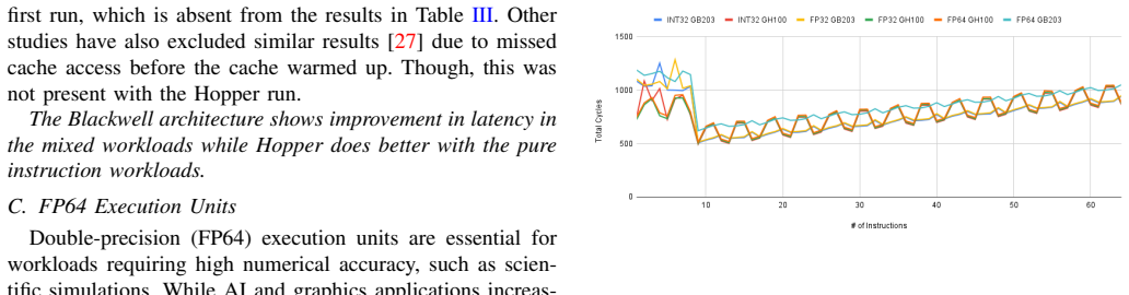
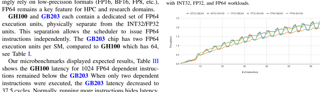
- On GB203, mixed INT32/FP32 workloads should see lower latency than on GH100, so developers can interleave integer and floating-point instructions without the penalty seen on older split-pipeline architectures.
- FP64 on Blackwell consumer GPUs is not a viable high-throughput path; scientific codes that need double precision should expect to emulate FP64 through FP32 or tensor-core paths, or run on Hopper-class hardware.
- Low-precision tensor-core users on Blackwell should be aware that FP4/FP6 inputs currently execute through QMMA (with FP4 as fallback) and that throughput is maximized with high ILP (around ILP=6) rather than large warp counts.
- Memory-bound kernels on GB203 should avoid strided access patterns that trigger bank conflicts in the smaller 128 KB L1/shared partition, while Hopper tolerates higher warp pressure in shared memory.
- For FP8 D-GEMM through cuBLASLt on the RTX 5080, current software yields lower throughput than Hopper, so developers should validate kernel selection or expect practical FP8 gains to appear only after software matures.
Reading between the lines
- If Blackwell's SASS mapping for FP4 is indeed a software fallback, a future CUDA release may switch FP4 to OMMA; the paper's power and throughput numbers for FP4 would then need re-measurement and could improve.
- The conclusion that GB203's scheduler favors high ILP suggests a testable porting rule: Blackwell kernels should be restructured to expose more independent mma operations per thread rather than relying on large active warp counts, and similar gains may appear on other Blackwell SKUs if the scheduler design is shared.
- The GB203/H100 comparison conflates architecture with memory technology (GDDR7 vs HBM2e) and SKU class; extending the same benchmarks to a datacenter Blackwell part (e.g., GB100) would separate what is Blackwell from what is consumer-GPU packaging.
- For compiler writers, the observed 1.21-cycle completion latency for all low-precision mma formats on GB203 suggests a single unified low-precision pipeline; instruction schedulers could treat FP4/FP6/FP8 mma identically for issue purposes.
Editorial analysis
A structured set of objections, weighed in public.
Referee Report
Summary. This paper presents a microbenchmark-based analysis of NVIDIA's Blackwell architecture, using the GeForce RTX 5080 (GB203) as the Blackwell representative and the H100 PCIe (GH100) as the Hopper baseline. The authors measure compute-pipeline latencies and throughputs for INT32/FP32/FP64, warp-scheduler behavior, the memory hierarchy (shared memory, L1, L2, global), and low-precision tensor-core operations (FP4, FP6, FP8), including power consumption. They also include two case studies: a dense FP8 GEMM and a Transformer inference workload. The central claim is that these microbenchmarks reveal subtle architectural differences between Blackwell and Hopper, providing guidance for developers and compiler writers.
Significance. If the measurements are correct, the paper is a useful addition to the empirical GPU microarchitecture literature, especially for the newly released Blackwell architecture. It reports concrete, falsifiable values (e.g., 4-cycle INT32/FP32 true latency, L1 hit latency of 30-40 cycles, L2 latency of 273/358 cycles on H100/RTX 5080) and cross-checks PTX instructions against generated SASS, which strengthens the methodology. The memory-hierarchy characterization and the explicit comparison of two product generations are valuable. However, the tensor-core section, which is a headline contribution, is undermined by the use of a software fallback path for FP4/FP6 and by confusion between latency and throughput metrics. The D-GEMM case study also contains a factor-of-1000 arithmetic error. These issues must be resolved before the paper's conclusions can be accepted.
major comments (5)
- [V.D] The FP4/FP6 tensor-core measurements characterize a compatibility/fallback path, not the native tcgen05/OMMA datapath. The paper itself states in Section V.A that the FP4 mma instruction produces QMMA SASS rather than the documented OMMA instruction, and calls QMMA "the fall back for FP4 inputs in the current software." Table IV also notes that tcgen05 is not supported for sm_120a. Consequently, the latency, throughput, and power values in Figures 4-5 and Table VI describe the behavior of the QMMA fallback path under the current CUDA toolchain, not the underlying 5th-generation tensor-core hardware. The conclusion in Section V.D that "Blackwell's warp scheduler is optimized for low-precision, high-ILP workloads" is therefore not supported by these data. The authors should either obtain measurements through the native path (e.g., by using the OMMA instructions they observed for FP8 with block scaling, or by using a toolchain that supports tcgen05 for sm_120a) or explicitly reframe the section as a study of current software behavior on Blackwell, with conclusions restricted accordingly.
- [V.D] The claimed "completion latency" of 1.21094 cycles for all mma formats at ILP=1 and one warp is implausible as a dependent-instruction latency for a matrix multiply accumulate. Per the paper's own definition in Section IV.A, completion latency is measured on a set of independent instructions and reported as cycles per instruction, which is a throughput-oriented quantity. For a single warp issuing a dependent chain of mma instructions, the latency from issue to data-ready is typically tens of cycles on NVIDIA GPUs. The reported value suggests that the measurement captures the issue interval (reciprocal throughput) rather than the completion latency of a dependent chain. Because Figure 5 is labeled "Latency" and the text in Section V.D uses this number to compare GB203 and GH100, the paper conflates throughput with latency. The authors should either measure true dependent-instruction latency (e.g., by chaining mma operations through the accumulator) or relabel and reinterpret the results as throughput measurements throughout the tensor-core section.
- [VII.A] The D-GEMM throughput values in Table VII are wrong by a factor of 1000. Using Equation (2) with the stated runtime of 4.710 ms for the RTX 5080 at M=N=K=8192, the throughput is 2*8192^3 / 0.00471 s = 2.33e14 FLOP/s = 233 TFLOPS, not 0.233 TFLOPS. The same error appears for all entries in the table (e.g., Hopper at 8192^3 should be roughly 887 TFLOPS, not 0.887 TFLOPS). The relative ordering is unchanged, but the absolute values are incorrect and mislead the reader about the actual performance levels. The authors must correct the unit conversion (milliseconds to seconds) and recalculate all values in Table VII and the corresponding text.
- [Introduction, Tables I-II, Sections VI.C-D] The cross-architecture comparison treats one consumer GPU (RTX 5080, GB203) as representative of Blackwell and one datacenter GPU (H100 PCIe, GH100) as representative of Hopper. These two SKUs differ not only in architecture but also in SM count, memory type (GDDR7 vs HBM2e), L2 size and partitioning, clock rates, TDP, and target market, as shown in Tables I and II. Several conclusions attribute observed differences to architectural choices rather than SKU configuration. For example, Section VI.C states that GH100's partitioned L2 is "optimized for high concurrency" while GB203's unified L2 "simplifies hardware complexity," and Section VI.D attributes the global-memory latency difference to HBM2e vs GDDR7, a memory-technology distinction rather than a Blackwell-vs-Hopper architectural one. To support these attributions, the authors should either restrict their claims to the specific products tested or explicitly discuss the confounds and justify why particular differences are architectural. Without such a caveat, the paper overgeneralizes from a two-point comparison.
- [Global] The paper states in Section I that "We are unable to share the code at this time due to the blind-review policy, but we plan to open-source it post the review process and the outcome." For an empirical microbenchmark paper whose entire contribution rests on measurements, this is a significant barrier to verification. Even during double-blind review, code can be provided as supplementary material without revealing author identity. The authors should either make the microbenchmarks available for the review process or provide a detailed experimental appendix covering kernel launch configurations, clock-frequency settings, power-measurement methodology (how nvidia-smi readings were aggregated), and the exact PTX/SASS snippets that underlie each key result. Without this, the load-bearing measurements (e.g., tensor-core latencies, memory latencies) cannot be independently checked.
minor comments (7)
- [Throughout] There are numerous typographical errors, including "Kelper" (Section II), "Turning" for Turing (Section II), "fmaand" (Section IV.B), "there respective architectures" (Section V.D), "stepper power curve" (Section VII.A), and "nv f p8 e4m3" (Section VII.A). A thorough proofread is needed.
- [Figure 11 caption] The caption says the 8192^3 Blackwell runtime (4.710 ms) was omitted from the graph, but the graph is supposed to show runtime across all sizes. Please explain why the point was omitted and consider including it in an inset or on a logarithmic axis so that the reader can see the full trend.
- [Table IV] The note "TCGEN05 IS YET TO BE SUPPORTED FOR THE ARCH. SM120A" appears as a detached all-caps line under the table. Integrate this into the surrounding text and elaborate on what it means for the experiments (e.g., which instructions were available and which were not).
- [Table VI] The header "POWER USAGE (WATTS)/PERFORMANCE PER WATT" is ambiguous. The body text describes the values as power consumption, so the header should be simply "Power usage (watts)". If performance-per-watt is also reported, separate columns are needed.
- [Section IV.A] "On GB203, without an instruction between the registers, the subtracted value is 1, compared to a value of 2 forGH100" is unclear. Clarify whether this is the overhead of the %clock64 measurement itself and how it was accounted for in later latency calculations.
- [Section V.D] The sentence "The maximum ILP level at which sustained throughput is achieved for each precision format, across decreasing warp counts is ILP=5 with 29 active warps, for GH100, and ILP=6 at 25 active warps, for GB203" is difficult to parse. Please rephrase to state the experimental procedure and the exact meaning of "maximum ILP level at which sustained throughput is achieved."
- [Section VII.B] The text says "with a from' 58.8W to 45W in FP8" in Section VII.B (Transformer inference); this appears to be a typo for "with a decrease from 58.8W to 45W."
Circularity Check
No significant circularity: direct microbenchmark measurements, external documentation grounding, and no load-bearing self-citations.
full rationale
This paper is an empirical measurement study. Every quantitative claim (latency, throughput, cache-boundary cycles, and power) is obtained by running PTX/CUDA microbenchmarks on two physical GPUs and reading clocks, timers, or nvidia-smi; there is no fitted parameter, no model whose adjustable constants are set from the data being 'predicted', and no derived quantity that is equal by construction to an input. The only reference to a co-author's prior work is [2], an instruction roofline model for AMD GPUs, cited in Related Work as an example of analytical performance modeling; none of the paper's conclusions depend on that citation. Reliance on NVIDIA PTX and CUDA Binary Utilities documentation for instruction names and SASS encodings is external grounding, not circularity. The observation that FP4 mma.sync currently lowers to QMMA rather than OMMA under CUDA 12.9, and the resulting caveat that FP4/FP6 measurements may describe a software fallback path, is a limitation on the strength of the tensor-core claims, not a circular derivation: the SASS instruction is independently observed, and the paper does not define Blackwell's tensor-core behavior in terms of its own conclusions. Cross-GPU attribution concerns (RTX 5080 vs H100 PCIe differ in memory type, L2 size, clocks, and TDP) are threats to comparability, not circularity. No self-citation chain, imported uniqueness theorem, or ansatz-smuggling is present.
Assumptions & free parameters
assumptions (5)
- domain assumption RTX 5080 (GB203) is treated as representative of the Blackwell architecture, and H100 PCIe (GH100) as representative of Hopper, so measured differences are attributed to architectural design rather than SKU configuration.
- domain assumption PTX microbenchmarks preserve the intended instruction streams and are not optimized away.
- domain assumption The %clock64-based measurement procedure yields true and completion latency values.
- domain assumption nvidia-smi power readings represent the power consumed by the workload under test.
- domain assumption D-GEMM results obtained through cuBLASLt reflect hardware tensor-core capability rather than library selection effects.
Cite this review
Pith. "Pith review of Dissecting the NVIDIA Blackwell Architecture with Microbenchmarks." pith.science (2026). https://pith.science/paper/ZODOOAJI
@misc{pith2026250710789,
  author       = {Pith},
  title        = {Pith review of: Dissecting the NVIDIA Blackwell Architecture with Microbenchmarks},
  year         = {2026},
  howpublished = {\url{https://pith.science/paper/ZODOOAJI}},
  note         = {Machine review of arXiv:2507.10789}
}
read the original abstract
The rapid development in scientific research provides a need for more compute power, which is partly being solved by GPUs. This paper presents a microarchitectural analysis of the modern NVIDIA Blackwell architecture by studying GPU performance features with thought through microbenchmarks. We unveil key subsystems, including the memory hierarchy, SM execution pipelines, and the SM sub-core units, including the 5th generation tensor cores supporting FP4 and FP6 precisions. To understand the different key features of the NVIDIA GPU, we study latency, throughput, cache behavior, and scheduling details, revealing subtle tuning metrics in the design of Blackwell. To develop a comprehensive analysis, we compare the Blackwell architecture with the previous Hopper architecture by using the GeForce RTX 5080 and H100 PCIe, respectively. We evaluate and compare results, presenting both generational improvements and performance regressions. Additionally, we investigate the role of power efficiency and energy consumption under varied workloads. Our findings provide actionable insights for application developers, compiler writers, and performance engineers to optimize workloads on Blackwell-based platforms, and contribute new data to the growing research on GPU architectures.
Figures

Figures from the paper (5 more)


Forward citations
Cited by 3 Pith papers
-
Sim-FA: A GPGPU Simulator Framework for Fine-Grained Asynchronous Pipeline Analysis
Sim-FA is a new simulator that instruments FlashAttention-3 for cycle-accurate GPGPU analysis, achieving 5.7% average error on H800 while explaining inaccuracies in existing DRAM traffic models.
-
Accurate Models of NVIDIA Tensor Cores
Software models of NVIDIA tensor cores reproduce GPU matrix-multiply results exactly on millions of random test inputs, for fp8/fp16/bf16/tf19 formats on nine GPU generations.
-
Accelerating Bidiagonalization of Banded Matrices through Memory-Aware Bulge-Chasing on GPUs
A memory-aware GPU bulge-chasing algorithm reduces banded matrices to bidiagonal form, achieving >100x speedups over CPU libraries at 32k sizes.
Reference graph
Works this paper leans on
-
[1]
Profiling general purpose gpu applications,
B. R. Coutinho, G. L. M. Teodoro, R. S. Oliveira, D. O. G. Neto, and R. A. C. Ferreira, “Profiling general purpose gpu applications,” in 2009 21st ISCA and HPC , 2009, pp. 11–18
work page 2009
-
[2]
Metrics and Design of an Instruction Roofline Model for AMD GPUs
M. Leinhauser, R. Widera, S. Bastrakov, A. Debus, M. Bussmann, and S. Chandrasekaran, “Metrics and design of an instruction roofline model for amd gpus,” 2021. [Online]. Available: https: //arxiv.org/abs/2110.08221
work page Pith review arXiv 2021
-
[3]
An analytical model for a gpu architecture with memory-level and thread-level parallelism awareness,
S. Hong and H. Kim, “An analytical model for a gpu architecture with memory-level and thread-level parallelism awareness,” SIGARCH Comput. Archit. News , vol. 37, no. 3, p. 152–163, Jun. 2009. [Online]. Available: https://doi.org/10.1145/1555815.1555775
arXiv 2009
-
[4]
Characterizing and improving the use of demand-fetched caches in gpus,
W. Jia, K. A. Shaw, and M. Martonosi, “Characterizing and improving the use of demand-fetched caches in gpus,” in Proceedings of the 26th ACM International Conference on Supercomputing , ser. ICS ’12. New York, NY , USA: ACM, 2012, p. 15–24. [Online]. Available: https://doi.org/10.1145/2304576.2304582
-
[5]
Demystifying gpu microarchitecture through microbenchmarking,
H. Wong, M.-M. Papadopoulou, M. Sadooghi-Alvandi, and A. Moshovos, “Demystifying gpu microarchitecture through microbenchmarking,” in 2010 ISPASS, 2010, pp. 235–246
work page 2010
-
[6]
Architectural analysis and performance characterization of nvidia gpus using microbenchmarking,
S. Subramoniapillai Ajeetha, “Architectural analysis and performance characterization of nvidia gpus using microbenchmarking,” Ph.D. dissertation, The Ohio State University, The Ohio State University,
-
[7]
Dissecting the NVIDIA volta GPU architecture via microbenchmarking,
Z. Jia, M. Maggioni, B. Staiger, and D. P. Scarpazza, “Dissecting the NVIDIA volta GPU architecture via microbenchmarking,” CoRR, vol. 1804.06826, 2018. [Online]. Available: http://arxiv.org/abs/1804.06826
arXiv 2018
-
[9]
Dissecting the nvidia hopper architecture through microbenchmarking and multiple level analysis,
W. Luo, R. Fan, Z. Li, D. Du, H. Liu, Q. Wang, and X. Chu, “Dissecting the nvidia hopper architecture through microbenchmarking and multiple level analysis,” 2025. [Online]. Available: https: //arxiv.org/abs/2501.12084
arXiv 2025
Show all 32 references
-
[10]
NVIDIA Corporation, NVIDIA H100 Tensor Core GPU Architecture , NVIDIA, Mar. 2022. [Online]. Available: https://resources.nvidia.com/ en-us-data-center-overview/gtc22-whitepaper-hopper
2022
-
[11]
——, NVIDIA Blackwell Architecture Technical Brief: Powering the New Era of Generative AI and Accelerated Computing , NVIDIA, Mar. 2024. [Online]. Available: https://resources.nvidia. com/en-us-blackwell-architecture
2024
-
[12]
Understanding data movement in tightly coupled heterogeneous systems: A case study with the grace hopper superchip,
L. Fusco, M. Khalilov, M. Chrapek, G. Chukkapalli, T. Schulthess, and T. Hoefler, “Understanding data movement in tightly coupled heterogeneous systems: A case study with the grace hopper superchip,”
-
[13]
[Online]
NVIDIA Corporation, NVIDIA RTX BLACKWELL GPU ARCHITECTURE, NVIDIA, 2025. [Online]. Avail- able: https://images.nvidia.com/aem-dam/Solutions/geforce/blackwell/ nvidia-rtx-blackwell-gpu-architecture.pdf
2025
-
[14]
Understanding the gpu microarchitecture to achieve bare-metal performance tuning,
X. Zhang, G. Tan, S. Xue, J. Li, K. Zhou, and M. Chen, “Understanding the gpu microarchitecture to achieve bare-metal performance tuning,” in Proceedings of the 22nd ACM SIGPLAN SPPPP , ser. PPoPP ’17. New York, NY , USA: ACM, 2017, p. 31–43. [Online]. Available: https://doi.o...
2017
-
[15]
Dissecting gpu memory hierarchy through mi- crobenchmarking,
X. Mei and X. Chu, “Dissecting gpu memory hierarchy through mi- crobenchmarking,” IEEE TPDS, vol. 28, no. 1, pp. 72–86, 2017
2017
-
[16]
Numerical behavior of NVIDIA tensor cores,
M. Fasi, N. J. Higham, M. Mikaitis, and S. Pranesh, “Numerical behavior of NVIDIA tensor cores,” PeerJ Computer Science , vol. 7, p. e330, 2021. [Online]. Available: https://doi.org/10.7717/peerj-cs.330
2021 doi
-
[17]
Fast implementation of dgemm on fermi gpu,
G. Tan, L. Li, S. Triechle, E. Phillips, Y . Bao, and N. Sun, “Fast implementation of dgemm on fermi gpu,” in Proceedings of SC 2011 , ser. SC ’11. New York, NY , USA: ACM, 2011. [Online]. Available: https://doi.org/10.1145/2063384.2063431
2011
-
[18]
Nvidia tensor core programmability, performance & precision,
S. Markidis, S. W. D. Chien, E. Laure, I. B. Peng, and J. S. Vetter, “Nvidia tensor core programmability, performance & precision,” in 2018 IEEE IPDPSW . IEEE, May 2018, p. 522–531. [Online]. Available: http://dx.doi.org/10.1109/IPDPSW.2018.00091
2018
-
[19]
Benchmarking the nvidia v100 gpu and tensor cores,
M. Martineau, P. Atkinson, and S. McIntosh-Smith, “Benchmarking the nvidia v100 gpu and tensor cores,” in Euro-Par 2018: Parallel Process- ing Workshops, G. Mencagli, D. B. Heras, V . Cardellini, E. Casalicchio, E. Jeannot, F. Wolf, A. Salis, C. Schifanella, R. R. Manumachu, L...
2018
-
[20]
Modeling deep learning accelerator enabled gpus,
M. A. Raihan, N. Goli, and T. M. Aamodt, “Modeling deep learning accelerator enabled gpus,” in 2019 IEEE ISPASS, 2019, pp. 79–92
2019
-
[21]
Demystifying tensor cores to optimize half-precision matrix multiply,
D. Yan, W. Wang, and X. Chu, “Demystifying tensor cores to optimize half-precision matrix multiply,” in 2020 IEEE International Parallel and Distributed Processing Symposium (IPDPS) , 2020, pp. 634–643
2020
-
[22]
Dissecting tensor cores via microbenchmarks: Latency, throughput and numeric behaviors,
W. Sun, A. Li, T. Geng, S. Stuijk, and H. Corporaal, “Dissecting tensor cores via microbenchmarks: Latency, throughput and numeric behaviors,” IEEE TPDS, vol. 34, no. 1, pp. 246–261, 2023
2023
-
[23]
Accel-sim: An extensible simulation framework for validated gpu modeling,
M. Khairy, Z. Shen, T. M. Aamodt, and T. G. Rogers, “Accel-sim: An extensible simulation framework for validated gpu modeling,” in 2020 ACM/IEEE 47th Annual International Symposium on Computer Architecture (ISCA), 2020, pp. 473–486
2020
-
[24]
Gcom: a detailed gpu core model for accurate analytical modeling of modern gpus,
J. Lee, Y . Ha, S. Lee, J. Woo, J. Lee, H. Jang, and Y . Kim, “Gcom: a detailed gpu core model for accurate analytical modeling of modern gpus,” in Proceedings of the 49th Annual ISCA , ser. ISCA ’22. New York, NY , USA: ACM, 2022, p. 424–436. [Online]. Available: https://doi....
2022
-
[25]
Llmperf: Gpu performance modeling meets large language models,
K. N. M. Nguyen, H. D. N. Do, H. T. Le, and T. T. Dao, “Llmperf: Gpu performance modeling meets large language models,” 2025. [Online]. Available: https://arxiv.org/abs/2503.11244
2025 arXiv
-
[26]
[Online]
NVIDIA Corporation, Parallel Thread Execution (PTX) ISA, Release 8.8, NVIDIA, 2025. [Online]. Available: https://docs.nvidia.com/cuda/ pdf/ptx isa 8.8.pdf
2025
-
[27]
A performance model for gpus with caches,
T. T. Dao, J. Kim, S. Seo, B. Egger, and J. Lee, “A performance model for gpus with caches,” IEEE TPDS, vol. 26, no. 7, pp. 1800–1813, 2015
2015
-
[28]
[Online]
NVIDIA Corporation, CUDA Binary Utilities - Instruction Set Reference, NVIDIA, 2025. [Online]. Available: https://docs.nvidia.com/ cuda/cuda-binary-utilities/index.html
2025
-
[29]
[Online]
——, NVIDIA TensorRT , https://developer.nvidia.com/tensorrt, 2024, version 10.0. [Online]. Available: https://developer.nvidia.com/tensorrt
2024
-
[30]
Gpt-neox- 20b: An open-source autoregressive language model,
S. Black, S. Biderman, E. Hallahan, Q. Anthony, L. Gao, L. Gold- ing, H. He, C. Leahy, K. McDonell, J. Phang et al. , “Gpt-neox- 20b: An open-source autoregressive language model,” arXiv preprint arXiv:2204.06745, 2022
2022 arXiv
-
[2012]
Available: http://rave.ohiolink.edu/etdc/view?acc num= osu1344623484
[Online]. Available: http://rave.ohiolink.edu/etdc/view?acc num= osu1344623484
-
[2019]
Available: http://arxiv.org/abs/1903.07486
[Online]. Available: http://arxiv.org/abs/1903.07486
1903 arXiv
-
[2024]
Available: https://arxiv.org/abs/2408.11556
[Online]. Available: https://arxiv.org/abs/2408.11556
Reviewed August 6, 2026 · model on record in the stance chip above.
Discussion (0). Sign in to comment.