REVIEW 4 major objections 5 minor 1 cited by
OpenGCRAM: An Open-Source Gain Cell Compiler Enabling Design-Space Exploration for AI Workloads
T0 review · 4 major / 5 minor · reviewed 2026-08-06 · deepseek-v4-flash
Pith's one-line read The paper presents OpenGCRAM, an open-source compiler that takes user memory specifications and produces gain-cell memory bank layouts for TSMC 40 nm, with HSPICE-verified area, delay, and power.
desk verdict OpenGCRAM is a real, useful step forward for open-source memory compilation of Si-Si GCRAM, but the OS-OS results are model-in-the-loop predictions rather than validated compiler output. read the letter →
The pith
A machine-rendered reading of the paper's core claim, the machinery that carries it, and where it could break.
The reading
What carries the argument
The central mechanism is the two-transistor gain cell, which stores a bit as charge on a storage node: one transistor writes through a write bitline when the write wordline is high, and a second transistor reads the stored charge onto a single-ended read bitline, so read and write are separate ports and no cross-coupled inverter pair is needed. The carrying architecture is OpenGCRAM's script-based compiler flow, in which user configuration drives automatic generation of the bitcell array, address and data peripherals, control logic, SPICE netlists, GDS layouts, and HSPICE measurement setups. For the OS-OS variant the load-bearing additions are a compact Verilog-A model of an ultra-low-leakage ITO transistor, calibrated against TCAD and one experimental device, and back-end-of-line layer definitions and design rules that let the two transistors be placed between tight-pitched metal layers on top of the silicon circuits.
What would settle it
Fabricate an OS-OS GCRAM bank from an OpenGCRAM-generated TSMC 40 nm layout and compare measured retention and leakage with the compiler's HSPICE predictions; if the ITO write transistor's off-state leakage is far above $10^{-18}$ A/µm or stored data does not persist for milliseconds at the specified operating voltage, the OS-OS claims are contradicted.
Extended reading notes
Core claim
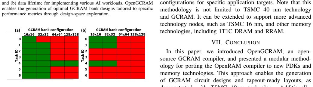
On its own terms, the paper establishes that SRAM-style compiler automation can be extended to gain-cell memories. OpenGCRAM generates a GCRAM bank from user parameters: a bitcell array of two-transistor cells with separate write and read wordlines and bitlines, dual-port address and data peripherals, an added reference generator for single-ended readout, and predischarge or precharge logic depending on the cell variant. The generated TSMC 40 nm banks pass DRC and LVS for capacities from 256 bits to 16 Kb, and the compiler automatically writes HSPICE stimuli to report operating frequency, effective bandwidth, leakage, and retention. The paper reports that a 2T Si-Si GCRAM bitcell is 31 percent smaller than a 6T SRAM cell, that an OS-OS GCRAM bitcell is 89 percent smaller, that the Si-Si GCRAM bank area is larger than SRAM at small capacities and becomes smaller only above roughly 256 Kb because of dual-port peripherals, and that OS-OS banks are smaller at all tested sizes. It also reports microsecond retention for Si-Si GCRAM, millisecond retention for OS-OS GCRAM with an ITO write transistor, and tunability beyond 10 seconds through threshold-voltage and material choices. Using an application-guided workload profiler, it constructs Shmoo plots, pass/fail maps over bank configuration and workload, showing which GCRAM bank sizes meet read-frequency and lifetime demands for L1 and L2 caches across seven AI workloads.
Load-bearing premise
The load-bearing premise is that the compact oxide-semiconductor transistor model, fitted to TCAD calibrated from a single measured ITO device, accurately predicts retention and leakage for the back-end-of-line transistors in a real TSMC 40 nm layout.
Editorial extensions
If this is right
- A chip team can go from a GCRAM configuration to a TSMC 40 nm layout that passes foundry design checks and to HSPICE area, delay, and power numbers without hand-laying-out analog blocks, greatly reducing memory design time.
- Because gain-cell read and write use separate ports, a generated GCRAM bank gives dual-port bandwidth, and bitcell leakage is nearly zero since there is no direct VDD-to-ground path, so on-chip memory power can fall well below SRAM.
- Retention can be matched to workload data lifetime, with microseconds for activation caches and seconds or longer for weight storage, by choosing threshold voltage, channel material, and whether a write-wordline level shifter is included.
- The porting methodology is not tied to one cell or process; the paper argues it extends to more advanced nodes and to other single-bitline memories such as 1T1C DRAM and RRAM, so the compiler could become a general memory-generation platform.
Reading between the lines
- A natural next step, not reported in this paper, is silicon measurement of an OpenGCRAM-generated bank; the compiler's OS-OS claims are currently backed by simulation through a TCAD-calibrated model rather than by a fabricated memory.
- The paper's main area comparison is dual-port GCRAM against single-port SRAM. Because a dual-port SRAM bank is roughly twice the area of a single-port one, a like-for-like comparison would make the GCRAM area crossover appear at smaller capacities.
- The Shmoo exploration assumes one bank per cache level. Extending the compiler to multibank GCRAM, listed as future work, may be the right response to the paper's finding that shared L2 caches demand much higher read frequency than per-core L1 caches.
- If the OS compact model is confirmed in silicon, OS-OS GCRAM's 11 percent-of-SRAM bitcell, placed in the back-end metal stack, would effectively add memory capacity on top of logic and change how much on-chip memory an accelerator can afford.
Editorial analysis
A structured set of objections, weighed in public.
Referee Report
Summary. The paper presents OpenGCRAM, an open-source memory compiler that extends the OpenRAM framework to generate gain-cell (GCRAM) memories. For a user-specified bank size, word width, and peripheral options, the compiler is claimed to produce SPICE netlists, GDS layouts, DRC/LVS-clean layout views, and HSPICE-based area/delay/power characterizations in TSMC 40nm. The authors describe a methodology for porting OpenRAM to new PDKs and memory types, then apply it to 2T Si-Si and 2T OS-OS GCRAM. Results include bitcell and bank area comparisons against SRAM, frequency/bandwidth/leakage simulations for Si-Si GCRAM, retention simulations for both variants, and a design-space exploration for AI cache workloads using the GainSight profiler.
Significance. If the central claims hold, OpenGCRAM would fill a real gap: researchers currently lack an open, automated, layout-generating GCRAM compiler, and the porting methodology could be reused for other PDKs and memory technologies. The paper gives explicit credit for its open-source release, its modular extension of OpenRAM, and its automatic HSPICE stimulus generation and simulation flow for Si-Si GCRAM. The design-space exploration for AI workloads is also a useful demonstration. However, the strongest OS-OS claims and the large-capacity area-crossover conclusion rest on projections and extrapolations rather than on validated compiler outputs, so the significance is conditional on the additional evidence requested below.
major comments (4)
- [V-A] The central claim that OpenGCRAM generates DRC/LVS-clean, tapeout-ready GCRAM layouts for TSMC 40nm is not supported by the evidence presented: Section V-A states that "we resolved all DRC and LVS errors" for bank sizes from 256 bits to 16Kb, but no DRC or LVS reports, error summaries, or rule-deck versions are shown, and no commit hash or artifact identifier is provided for the released code. Since this claim is load-bearing for the paper's main contribution, the authors should supply the actual check reports (or a reproducible script that regenerates them) and a pinned repository version; without these, a reader cannot verify that the layouts are clean or reproduce the result.
- [V-D, VI] The OS-OS GCRAM results—ultra-low leakage (<1e-18 A/µm), 89% area reduction, millisecond retention, and the Shmoo design space in Fig. 10—rest on a Verilog-A compact model that was fitted to TCAD results, and the TCAD was calibrated using a single experimental ultra-low-leakage ITO transistor (Section V-D). No evidence is given that this device is representative of the BEOL OS transistors assumed in the TSMC 40nm layout, and Section VI states that HSPICE simulation of OS-OS banks is future work, so operating frequency, bandwidth, and power for OS-OS are not evaluated by the compiler. These OS-OS conclusions should be presented as model-based projections with a clear statement of the underlying assumptions, and ideally validated against an OS device fabricated in the target BEOL or against foundry-supported OS device models.
- [V-B, Fig. 6(c)] The claim that Si-Si GCRAM bank area becomes smaller than SRAM for bank sizes beyond 256 Kb is based on polynomial trendlines extrapolated from only three simulated bank sizes (1, 4, and 16 Kb) in Fig. 6(c). Polynomial extrapolation over two orders of magnitude is not justified without error bounds, goodness-of-fit measures, or generated layouts at larger capacities, and the plotted comparison is against single-port SRAM even though the GCRAM banks are dual-port; the authors note that a fair dual-port SRAM comparison would roughly double the SRAM area, but this is not reflected in the figure. The crossover claim should be reworded as a projection or supported by actual compiler runs at larger bank sizes.
- [V-E, Fig. 10] The Shmoo plots in Fig. 10 claim to show whether a GCRAM bank can work for each L1/L2 cache task, but the text does not define the success criterion (e.g., frequency margin, retention versus required data lifetime, write/read timing, or noise margin). Without a precise definition of what makes a configuration "work," the design-space exploration results are difficult to interpret or reproduce. The authors should state the pass/fail metric and the simulation conditions used to generate the Shmoo plots.
minor comments (5)
- [I, VI] There are several typos that should be corrected, including "ABSRTACT" in Section I and "bandiwdth" in Section VI.
- [V-D, Fig. 8] The caption for Fig. 8 labels two subfigures as "(d)"; the second one should be "(e)", and the text should be checked for corresponding cross-references.
- [References] References [6] and [27] are duplicate entries for the same paper; please consolidate and renumber.
- [Footnote 1] The footnote states that the TSMC 40nm tech script and proprietary custom cells are protected by NDA; for reproducibility, please provide a manifest of which parts of the repository are included versus NDA-protected, and add a commit hash to the arXiv version.
- [Fig. 7] The green data points used in Fig. 7(a) may be hard to distinguish in black-and-white print; consider using distinct marker shapes or gray shading.
Circularity Check
No significant circularity: OpenGCRAM's compiler flow is validated against DRC/LVS and OpenRAM-style generation, and the OS-OS retention claim is a model-based simulation rather than a self-referential prediction.
full rationale
The paper's central contribution is an open-source compiler that extends OpenRAM to GCRAM with TSMC 40nm DRC/LVS-clean layout generation and HSPICE simulation for Si-Si GCRAM. The derivation chain for area, frequency, bandwidth, and leakage comparisons is based on generated netlists, automatically produced layouts, and standard DRC/LVS checks, not on a self-defined target. The OS-OS retention results (Section V-D) are explicitly presented as simulations using a Verilog-A compact model 'calibrated ... to fit the TCAD results,' with TCAD calibrated against an experimental ITO transistor; this is a conventional model-fitting flow in which the fitted target is the device I-V behavior, while retention is a downstream circuit-level simulation, so the retention number is not equivalent to the fit input by construction. The GainSight profiler [26] is a same-author tool used to supply workload cache requirements; it is an external input to the design-space exploration and does not define the compiler's correctness. The paper's own Future Work section concedes that OS-OS HSPICE frequency/bandwidth/power simulation is not yet implemented, which is a completeness limitation rather than a circularity. No load-bearing argument reduces to a self-citation or to a parameter renamed as a prediction.
Assumptions & free parameters
free parameters (2)
- OS transistor compact model parameters =
not reported (fit to TCAD results)
- Polynomial trendline coefficients for area extrapolation =
not reported (fit to 1-16 Kb data)
assumptions (5)
- domain assumption OpenRAM's memory compiler architecture can be generalized to single-ended GCRAM with separate read/write ports without loss of correctness.
- domain assumption HSPICE simulations using TSMC 40nm PDK models accurately predict the frequency, power, and retention of generated GCRAM banks.
- ad hoc to paper The Verilog-A compact model for the ITO OS transistor, calibrated to TCAD of an experimental transistor, is representative of the BEOL OS devices in the generated OS-OS GCRAM layout.
- domain assumption Passing DRC and LVS is sufficient to call a layout tapeout-ready.
- domain assumption GainSight profiling on NVIDIA H100 scaled to GT 520M accurately captures L1/L2 cache read frequency and lifetime demands of the listed AI workloads.
Cite this review
Pith. "Pith review of OpenGCRAM: An Open-Source Gain Cell Compiler Enabling Design-Space Exploration for AI Workloads." pith.science (2026). https://pith.science/paper/3SKSP753
@misc{pith2026250710849,
  author       = {Pith},
  title        = {Pith review of: OpenGCRAM: An Open-Source Gain Cell Compiler Enabling Design-Space Exploration for AI Workloads},
  year         = {2026},
  howpublished = {\url{https://pith.science/paper/3SKSP753}},
  note         = {Machine review of arXiv:2507.10849}
}
read the original abstract
Gain Cell memory (GCRAM) offers higher density and lower power than SRAM, making it a promising candidate for on-chip memory in domain-specific accelerators. To support workloads with varying traffic and lifetime metrics, GCRAM also offers high bandwidth, ultra low leakage power and a wide range of retention times, which can be adjusted through transistor design (like threshold voltage and channel material) and on-the-fly by changing the operating voltage. However, designing and optimizing GCRAM sub-systems can be time-consuming. In this paper, we present OpenGCRAM, an open-source GCRAM compiler capable of generating GCRAM bank circuit designs and DRC- and LVS-clean layouts for commercially available foundry CMOS, while also providing area, delay, and power simulations based on user-specified configurations (e.g., word size and number of words). OpenGCRAM enables fast, accurate, customizable, and optimized GCRAM block generation, reduces design time, ensure process compliance, and delivers performance-tailored memory blocks that meet diverse application requirements.
Figures


Figures from the paper (6 more)


Forward citations
Cited by 1 Pith paper
-
Reducing Power Consumption of Embedded Dynamic Memories with ECCs
For retention-limited GCRAM, the minimum-power ECC is workload-dependent — strong BCH codes win when refresh dominates, light codes win under heavy access — giving modeled total-power reductions of 46.8-94.8%.
Reference graph
Works this paper leans on
-
[1]
A. Gholami, Z. Yao, S. Kim, C. Hooper, M. W. Mahoney, and K. Keutzer, “AI and Memory Wall,”IEEE Micro, vol. 44, no. 3, pp. 33–39, May 2024, conference Name: IEEE Micro. [Online]. Available: https://ieeexplore.ieee.org/abstract/document/10477550
-
[2]
R. Saligram, S. Datta, and A. Raychowdhury, “Cryomem: A 4k-300k 1.3 ghz edram macro with hybrid 2t-gain-cell in a 28nm logic process for cryogenic applications,” in2021 IEEE Custom Integrated Circuits Conference (CICC). IEEE, 2021, pp. 1–2
work page 2021
-
[3]
S. Liu, S. Li, Q. Lin, K. Jana, S. Mitra, H.-S. P. Wong, and K. Toprasert- pong, “Hybrid 2t nmos/pmos gain cell memory with indium-tin-oxide and carbon nanotube mosfets for counteracting capacitive coupling,” IEEE Electron Device Letters, 2023
work page 2023
-
[4]
S. Liu, K. Jana, K. Toprasertpong, J. Chen, Z. Liang, Q. Jiang, S. Wahid, S. Qin, W.-C. Chen, and H.-S. P. Wong, “Gain cell memory on logic platform–device guidelines for oxide semiconductor transistor materials development,” in2023 International Electron Devices Meeting (IEDM). IEEE, 2023, pp. 1–4
work page 2023
-
[5]
W.-S. Khwa, P.-C. Wu, J.-J. Wu, J.-W. Su, H.-Y . Chen, Z.-E. Ke, T.-C. Chiu, J.-M. Hsu, C.-Y . Cheng, Y .-C. Chenet al., “34.2 a 16nm 96kb integer/floating-point dual-mode-gain-cell-computing-in-memory macro achieving 73.3-163.3 tops/w and 33.2-91.2 tflops/w for ai-edge devices,” in2024 IEEE International Solid-State Circuits Conference (ISSCC), vol. 67. ...
work page 2024
-
[7]
A 1-mbit fully logic-compatible 3t gain-cell embedded dram in 16-nm finfet,
R. Giterman, A. Shalom, A. Burg, A. Fish, and A. Teman, “A 1-mbit fully logic-compatible 3t gain-cell embedded dram in 16-nm finfet,” IEEE Solid-State Circuits Letters, vol. 3, pp. 110–113, 2020
work page 2020
-
[8]
R. Giterman, A. Fish, A. Burg, and A. Teman, “A 4-transistor nmos-only logic-compatible gain-cell embedded dram with over 1.6-ms retention time at 700 mv in 28-nm fd-soi,”IEEE Transactions on Circuits and Systems I: Regular Papers, vol. 65, no. 4, pp. 1245–1256, 2017
work page 2017
-
[9]
H. Ye, J. Gomez, W. Chakraborty, S. Spetalnick, S. Dutta, K. Ni, A. Raychowdhury, and S. Datta, “Double-gate w-doped amorphous indium oxide transistors for monolithic 3d capacitorless gain cell edram,” in2020 IEEE International Electron Devices Meeting (IEDM). IEEE, 2020, pp. 28–3
work page 2020
Show all 26 references
-
[10]
Openram: An open-source memory compiler,
M. R. Guthaus, J. E. Stine, S. Ataei, B. Chen, B. Wu, and M. Sarwar, “Openram: An open-source memory compiler,” in2016 IEEE/ACM International Conference on Computer-Aided Design (ICCAD), 2016, pp. 1–6
2016
-
[11]
R. M. Technologies. (2020) Gcram. [Online]. Available: https: //raaam-tech.com/technology/
2020
-
[12]
Gain-cell embedded drams: Modeling and design space,
A. Bonetti, R. Golman, R. Giterman, A. Teman, and A. Burg, “Gain-cell embedded drams: Modeling and design space,”IEEE Transactions on Very Large Scale Integration (VLSI) Systems, vol. 28, no. 3, pp. 646–659, 2020
2020
-
[13]
Design and optimization of a low power voltage reference generator circuit in 45nm cmos technology,
R. Singh, S. Singhal, and A. K. Singh, “Design and optimization of a low power voltage reference generator circuit in 45nm cmos technology,” International Journal Of Innovative Research & Development, vol. 3, 2014
2014
-
[14]
A 1.1 v, 667mhz random cycle, asymmetric 2t gain cell embedded dram with a 99.9 percentile retention time of 110µsec,
K. C. Chun, P. Jain, T.-H. Kim, and C. H. Kim, “A 1.1 v, 667mhz random cycle, asymmetric 2t gain cell embedded dram with a 99.9 percentile retention time of 110µsec,” in2010 Symposium on VLSI Circuits. IEEE, 2010, pp. 191–192
2010
-
[15]
First experimental demonstration of hybrid gain cell memory with si pmos and ito fet for high-speed on-chip memory,
S. Liu, S. Qin, K. Jana, J. Chen, K. Toprasertpong, and H.-S. P. Wong, “First experimental demonstration of hybrid gain cell memory with si pmos and ito fet for high-speed on-chip memory,” in2024 IEEE Symposium on VLSI Technology and Circuits (VLSI Technology and Circuits). IE...
2024
-
[16]
Automated synthesis of multi-port memories and control,
H. Nichols, M. Grimes, J. Sowash, J. Cirimelli-Low, and M. R. Guthaus, “Automated synthesis of multi-port memories and control,” in2019 IFIP/IEEE 27th International Conference on Very Large Scale Integra- tion (VLSI-SoC). IEEE, 2019, pp. 59–64
2019
-
[17]
First demonstration of dual-gate igzo 2t0c dram with novel read operation, one bit line in single cell, i on= 1500 µa/µm@ v ds= 1v and retention time¿ 300s,
W. Lu, Z. Zhu, K. Chen, M. Liu, B.-M. Kang, X. Duan, J. Niu, F. Liao, W. Dan, X.-S. Wuet al., “First demonstration of dual-gate igzo 2t0c dram with novel read operation, one bit line in single cell, i on= 1500 µa/µm@ v ds= 1v and retention time¿ 300s,” in2022 International Ele...
2022
-
[18]
Wkvquant: Quantizing weight and key/value cache for large language models gains more,
Y . Yue, Z. Yuan, H. Duanmu, S. Zhou, J. Wu, and L. Nie, “Wkvquant: Quantizing weight and key/value cache for large language models gains more,”arXiv preprint arXiv:2402.12065, 2024
2024 arXiv
-
[19]
Auto-tuning a high-level language targeted to gpu codes,
S. Grauer-Gray, L. Xu, R. Searles, S. Ayalasomayajula, and J. Cavazos, “Auto-tuning a high-level language targeted to gpu codes,” in2012 innovative parallel computing (InPar). Ieee, 2012, pp. 1–10
2012
-
[20]
Polyhedral-based data reuse optimization for configurable computing,
L.-N. Pouchet, P. Zhang, P. Sadayappan, and J. Cong, “Polyhedral-based data reuse optimization for configurable computing,” inProceedings of the ACM/SIGDA international symposium on Field programmable gate arrays, 2013, pp. 29–38
2013
-
[21]
Mlperf inference benchmark,
V . J. Reddi, C. Cheng, D. Kanter, P. Mattson, G. Schmuelling, C.-J. Wu, B. Anderson, M. Breughe, M. Charlebois, W. Chouet al., “Mlperf inference benchmark,” in2020 ACM/IEEE 47th Annual International Symposium on Computer Architecture (ISCA). IEEE, 2020, pp. 446– 459
2020
-
[22]
Llama: Open and efficient foundation language models,
H. Touvron, T. Lavril, G. Izacard, X. Martinet, M.-A. Lachaux, T. Lacroix, B. Rozi `ere, N. Goyal, E. Hambro, F. Azharet al., “Llama: Open and efficient foundation language models,”arXiv preprint arXiv:2302.13971, 2023
2023 arXiv
-
[23]
Deep Residual Learning for Image Recognition,
K. He, X. Zhang, S. Ren, and J. Sun, “Deep Residual Learning for Image Recognition,” Dec. 2015, arXiv:1512.03385 [cs]. [Online]. Available: http://arxiv.org/abs/1512.03385
2015 arXiv
-
[24]
Bert: Pre-training of deep bidirectional transformers for language understanding,
J. Devlin, M.-W. Chang, K. Lee, and K. Toutanova, “Bert: Pre-training of deep bidirectional transformers for language understanding,” inPro- ceedings of the 2019 conference of the North American chapter of the association for computational linguistics: human language technolog...
2019
-
[25]
Scaling rectified flow transformers for high-resolution image synthesis,
P. Esser, S. Kulal, A. Blattmann, R. Entezari, J. M ¨uller, H. Saini, Y . Levi, D. Lorenz, A. Sauer, F. Boeselet al., “Scaling rectified flow transformers for high-resolution image synthesis,” inForty-first international conference on machine learning, 2024
2024
-
[26]
GainSight: Application- Guided Profiling for Composing Heterogeneous On-Chip Memories in AI Hardware Accelerators,
P. Li, M. Hung, Y . Tan, K. Hoßfeld, J. J. Cheng, S. Liu, L. Yan, X. Wang, H.-S. P. Wong, and T. Tambe, “GainSight: Application- Guided Profiling for Composing Heterogeneous On-Chip Memories in AI Hardware Accelerators,” Apr. 2025, arXiv:2504.14866 [cs]. [Online]. Available: h...
2025 arXiv
-
[27]
A 667 mhz logic- compatible embedded dram featuring an asymmetric 2t gain cell for high speed on-die caches,
K. C. Chun, P. Jain, T.-H. Kim, and C. H. Kim, “A 667 mhz logic- compatible embedded dram featuring an asymmetric 2t gain cell for high speed on-die caches,”IEEE Journal of Solid-State Circuits, vol. 47, no. 2, pp. 547–559, 2011
2011
Reviewed August 6, 2026 · model on record in the stance chip above.
Discussion (0). Continue with ORCID to comment.