REVIEW 4 major objections 3 minor 1 cited by
SuperSNN: A Hardware-Aware Framework for Physically Realizable, High-Performance Superconducting Spiking Neural Network Chips
T0 review · 4 major / 3 minor · reviewed 2026-08-05 · deepseek-v4-flash
Pith's one-line read Superconducting spiking chip classifies digits at 80% accuracy
desk verdict A tapeout-level design and training framework for a tiny superconducting SNN, but the fabricated-chip accuracy is unverified and internally inconsistent; worth a referee's time only if the authors can produce measured data. read the letter →
The pith
A machine-rendered reading of the paper's core claim, the machinery that carries it, and where it could break.
The reading
What carries the argument
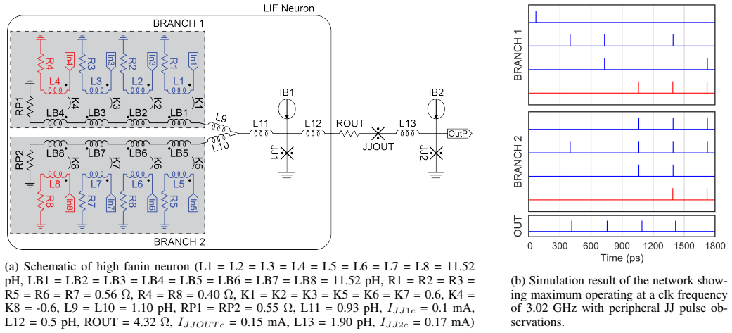
The load-bearing piece is the high fan-in neuron cell: eight mutually coupled input branches (six positive, two negative) drive a single Josephson junction through two dendritic bundles, so weighted summation happens by current addition in superconducting loops. Standardizing every neuron to exactly eight inputs keeps the layout regular and reusable. Around that cell, a locally asynchronous, globally synchronous (LAGS) clock distribution coordinates pulse arrival times across passive transmission lines, while a 49-bit shift register reduces the 7×7 input to seven pins at the cost of a several-cycle loading delay.
What would settle it
Directly bench-test the fabricated chip: feed the recorded 7×7 MNIST test samples through the seven input pins, capture the three output pins over many cycles, and compare the resulting classifications to the software model. If the chip's accuracy is statistically indistinguishable from chance (33%) for digits 2, 3, and 4, or if no output pulses appear at the claimed clock rate, the central claim fails.
Extended reading notes
Core claim
The central claim is that physical realizability constraints need not be treated as an afterthought in superconducting neural network design. SuperSNN folds those constraints into the network itself: weights are restricted to +1, 0, and −1, each neuron's fan-in is capped to fit the silicon area, and the resulting discrete connections map directly onto a high fan-in neuron cell in which synaptic currents add magnetically at a single Josephson junction. The framework trains two networks—a large one for the full MNIST benchmark and a small one that obeys the 40-pin, 25-neuron chip limits—and then lays out the small one using standard cells, a shift-register input scheme, and a clock distributio
Load-bearing premise
The core result depends on the fabricated chip actually performing the trained classification at the reported 80.07% accuracy and 3.02 GHz operation, yet the paper includes no measured test protocol, output waveforms, or per-class spike counts, so those numbers may reflect simulation rather than chip measurements.
Editorial extensions
If this is right
- A full inference SNN, not just a few neurons, can be placed on a single superconducting chip under real fabrication constraints.
- The 40-pin limit can be met by serial shift-register input, at the price of a reduced classification throughput.
- The per-inference energy of 6.55 fJ and 2.15 mW static power suggest cryogenic inference far more efficient than CMOS, if the reported figures are reproduced.
- The accuracy gap between the full network (96.47%) and the chip (80.07%) comes primarily from 7×7 downsampling and pin limits, not from the neuron cell itself.
- The same framework can be retargeted to other digit subsets; digits 0, 1, and 2 yield 86.2% accuracy.
Reading between the lines
- The 7×7 downsampling is likely the dominant accuracy loss; moving to 14×14 inputs or adding a convolutional front-end would probably close much of the gap, but would require more pins and a larger neuron fan-in.
- The reported 3.02 GHz clock frequency appears to be a simulation or schematic estimate, because the shift-register path is described as adding 433 ps, which implies a throughput ceiling near 1 GHz for the actual chip.
- The 6.55 fJ per-inference figure implies that only a small fraction of the 5,822 Josephson junctions switch during a single classification; counting switching events in the simulation netlist would test this.
- The same training and neuron-cell recipe could be run on a non-MNIST dataset, such as Fashion-MNIST or EMNIST letters, to check whether the accuracy holds beyond handwritten digits.
Editorial analysis
A structured set of objections, weighed in public.
Referee Report
Summary. The paper introduces SuperSNN, an end-to-end framework for designing physically realizable superconducting spiking neural networks under MIT LL SFQ5ee constraints. It combines hardware-aware training (pruning, weight quantization, hybrid spike/membrane loss), custom SFQ cells including a high fan-in neuron, a shift-register input scheme, and a locally synchronous/globally synchronous (LAGS) clock distribution. The authors report a complete MNIST network with 96.47% accuracy after quantization/pruning and a fabricated chip for digits 2/3/4 with claimed hardware accuracies of 80.07% (abstract, Table VI) and 86.2% (Abstract, Table V, §4.3), operating at 3.02 GHz, with 5,822 JJs, 2.15 mW static power, and 6.55 fJ per inference. The central claim is that a full SFQ SNN chip was fabricated and successfully classified MNIST subsets.
Significance. If the fabricated-chip results are genuine and reproducible, this would be a notable advance in superconducting neuromorphic hardware: it would demonstrate a complete, physically realized SFQ SNN within a commercial fabrication process, with an extremely high clock rate and low energy per inference. The framework contributions—quantization-aware training, fan-in/fan-out constrained layout, and the LAGS clocking scheme—are valuable and partially verified through layout and circuit simulation. However, the significance is heavily contingent on the chip measurements, which are not reported. The paper also provides concrete resource counts (JJs, area, power) that would be useful to the community if properly backed.
major comments (4)
- [Abstract; §4.2; §4.3; Fig. 3(b)] The headline result—'the fabricated SuperSNN chip successfully classified a reduced set of digits with 80.07% accuracy'—is not supported by any measured chip data. Section 4.2 describes implementation and timing but gives no test setup, no description of how output DC levels are converted to labels, no raw output traces, no confusion matrix, and no list of test images. The 3.02 GHz operating point is attributed to Fig. 3(b), whose caption explicitly states 'Simulation result', not chip measurement. The 6.55 fJ per inference is described in the Conclusion as 'estimated switching energy'. Thus the central empirical claim—that the chip physically realized the trained network—is unverified in this manuscript.
- [Abstract vs Table V and §4.3] There is an internal inconsistency about the fabricated chip's accuracy. The abstract states 80.07% for digits 2/3/4 and 'maximum 86.2% for digits 0/1/2', and Table VI reports 86.20% for 0/1/2 and 80.07% for 2/3/4. However, Table V lists 'Accuracy (%)' as 86.2 for the row 'Predictable digits 2, 3, 4', and §4.3 states that the prototype 'focuses on the digit subset 2, 3, and 4, achieving an inference accuracy of 86.2%'. The reader cannot determine which number was observed on the fabricated chip, on which test set, or whether 86.2% refers to the 2/3/4 chip at all. This must be corrected with an unambiguous mapping between digit subsets and accuracies.
- [§3.1.1(e); §4.1] The complete-network accuracy of 96.47% is obtained after a training procedure that selects the model with the highest accuracy on the full test dataset: 'Each stage runs for a predetermined number of epochs, with the model yielding the highest accuracy on the full test dataset being preserved' (stage e, Validation). This is test-set leakage/model selection on the test set, which inflates the reported accuracy and makes the 96.47% figure not an honest estimate of generalization. A held-out validation set must be used for model selection, and the test set should be used only once for final evaluation. This issue affects the correctness of the complete-network claim.
- [§4.3; Conclusion] The power and energy figures—2.15 mW static power, 6.55 fJ per inference, and 1.31e-6 nJ—are presented as chip characteristics, but the manuscript does not provide any measurement methodology or instrument details. The conclusion explicitly calls the switching energy 'estimated'. If these are simulation or schematic estimates, they should be labeled as such throughout, and the distinction between simulated and measured quantities must be made explicit in the abstract and results tables. As written, a reader may reasonably but incorrectly infer that these values were measured from the fabricated chip.
minor comments (3)
- [Abstract vs Introduction/Contributions] The clock scheme is called 'locally synchronous, globally synchronous (LAGS)' in the Abstract but 'locally asynchronous, globally synchronous (LAGS)' in the Introduction's contribution list. Please standardize the terminology and clarify the actual synchronization policy.
- [Conclusion] The conclusion says 'after quantification and pruning' where 'quantization' is meant. Please fix this typo.
- [Reference [25]] Reference [25] is dated 2020 in the text but the arXiv ID (1812.10354) suggests a 2018 preprint. Please verify the citation details.
Circularity Check
No circular derivation: accuracies come from external MNIST test labels and circuit simulations; the cited prior neuron cell [26] is independent published work, and the missing chip measurement is an evidence gap, not a circularity.
full rationale
The derivation chain is self-contained against external benchmarks. The complete-network and chip-network accuracies (96.47%, 86.2%, 80.07%) are trained/evaluated with snnTorch on the MNIST test set after binarization, quantization, and pruning; the labels are external, so no equation reduces to its own input. The 3.02 GHz figure is explicitly a circuit simulation (Fig. 3(b): 'Simulation result of the network showing maximum operating at a clk frequency of 3.02 GHz'), and the 6.55 fJ is described in the conclusion as 'estimated switching energy,' not as a fitted parameter renamed as a prediction. The 'six positive, two negative' fan-in structure is extracted from the trained model and then imposed as a hardware constraint; this is a design choice, and accuracy is subsequently measured under that constraint, so it is not a fitted input called a prediction. The only notable self-citation is [26] for the high fan-in neuron cell and the JTL timing detail; [26] is a peer-reviewed, externally published design with its own simulation support, and the present paper also provides its own layout and simulation, so this is not a load-bearing circular self-citation chain. I do flag a serious evidence gap: the abstract and Section 4.3 state that the fabricated chip 'successfully classified' digits (80.07%) and 'reports a fabricated superconducting SNN prototype ... achieving an inference accuracy of 86.2%,' but no measured test protocol, raw classification outputs, output waveforms, or measured clock/power/energy data are provided; the numbers in Table VI appear to be software-evaluated accuracies and the 80.07%/86.2% assignment is internally inconsistent between abstract, Table V, and Section 4.3. This is a correctness/verifiability problem, not a circularity problem, because no derivation is equivalent to its input by construction.
Assumptions & free parameters
free parameters (7)
- LIF decay beta (Eq. 2)
- Loss weight ratio L_spike:L_mem =
0.6 : 0.4
- Input downsampling binarization threshold =
0.3
- Simulation time steps =
25 for complete network; 1 forward pass for chip network
- Chip neuron fan-in structure =
6 positive, 2 negative per neuron
- Complete-network per-neuron fan-in limit =
64 connections per neuron
- Neuron threshold and circuit component values =
L1..L8 = 11.52 pH, R1..R3 = 0.56 ohm, R4/R8 = 0.40 ohm, K = +/-0.6, JJ Ic = 0.1-0.17 mA
assumptions (4)
- domain assumption The LIF hard-reset model (Eq. 2) matches the fabricated high fan-in neuron behavior.
- domain assumption The SFQ standard cells (DFF, JTL, PTL, splitters) behave at 3.02 GHz with the LAGS clock distribution.
- domain assumption The reported chip test classification reflects the trained weights.
- domain assumption 7x7 downsampled, binarized inputs preserve enough information for the chosen digit triples.
Cite this review
Pith. "Pith review of SuperSNN: A Hardware-Aware Framework for Physically Realizable, High-Performance Superconducting Spiking Neural Network Chips." pith.science (2026). https://pith.science/paper/FMFTENEP
@misc{pith2026250905532,
  author       = {Pith},
  title        = {Pith review of: SuperSNN: A Hardware-Aware Framework for Physically Realizable, High-Performance Superconducting Spiking Neural Network Chips},
  year         = {2026},
  howpublished = {\url{https://pith.science/paper/FMFTENEP}},
  note         = {Machine review of arXiv:2509.05532}
}
read the original abstract
Despite numerous proposed designs for superconducting neural networks (SNNs), most have overlooked practical fabrication constraints, leading to implementations limited to only a few neurons or synapses. Current superconducting technologies, such as MIT LL SFQ5ee, impose severe limitations on chip area, routing, and input/output pin counts (e.g., 5x5 mm^2 chip with 40 pins), drastically restricting network size and complexity. These hardware constraints necessitate a comprehensive framework to tailor network designs for physical realizability while minimizing accuracy loss. This paper introduces SuperSNN, a comprehensive framework for the implementation of full superconducting SNNs on a chip within these constraints. The key technical contributions include: (1) A hardware-aware training methodology for SNNs, utilizing off-chip pruning and weight quantization for energy-efficient superconducting implementations. (2) Design and layout of an inference SNN chip that incorporates novel high fan-in neurons and custom superconducting cells. (3) An optimized locally synchronous, globally synchronous (LAGS) clock distribution scheme for robust circuit implementation and management of data transfer delays in SFQ SNNs. The main results and findings demonstrate the effectiveness of the framework: (1) The complete network achieved 96.47% accuracy on the full MNIST dataset after quantization and pruning. (2) The fabricated SuperSNN chip successfully classified a reduced set of digits (2, 3, and 4) with 80.07% accuracy, reaching a maximum of 86.2% accuracy for digits 0, 1, and 2. (3) The chip operates at an ultra-high 3.02 GHz clock frequency. (4) It occupies a compact area of 3.4 x 3.9 mm^2, incorporates 5,822 Josephson Junctions, consumes 2.15 mW static power, and has an exceptionally low energy cost of 6.55 fJ (or 1.31e-6 nJ) per inference.
Figures


Figures from the paper (5 more)


Forward citations
Cited by 1 Pith paper
-
Programmable superconducting neuron with intrinsic in-memory computation and dual-timescale plasticity for ultra-efficient neuromorphic computing
A programmable superconducting LIF neuron with intrinsic static memory and dual-timescale plasticity achieves 45 GHz operation and femtojoule energy per spike.
Reference graph
Works this paper leans on
-
[1]
Hardware implementation of spiking neural networks on fpga,
J. Han, Z. Li, W. Zheng, and Y . Zhang, “Hardware implementation of spiking neural networks on fpga,”Tsinghua Science and Technology, vol. 25, no. 4, pp. 479–486, 2020
work page 2020
-
[2]
Optical neural networks: progress and challenges,
T. Fu, J. Zhang, R. Sun, Y . Huang, W. Xu, S. Yang, Z. Zhu, and H. Chen, “Optical neural networks: progress and challenges,”Light: Science & Applications, vol. 13, no. 1, p. 263, Sep. 2024. [Online]. Available: https://www.nature.com/articles/s41377-024-01590-3
work page 2024
-
[3]
F. Cai, S. Kumar, T. Vaerenbergh, X. Sheng, R. Liu, C. Li, Z. Liu, M. Foltin, S. Yu, Q. Xia, J. J. Yang, R. Beausoleil, W. Lu, and J. P. Strachan, “Power-efficient combinatorial optimization using intrinsic noise in memristor hopfield neural networks,”Nature Electronics, vol. 3, pp. 1–10, 07 2020
work page 2020
-
[4]
Cresti,Beyond-CMOS: State of the Art and Trends, ser
A. Cresti,Beyond-CMOS: State of the Art and Trends, ser. ISTE Consignment. Wiley, 2023. [Online]. Available: https://books.google.com/books?id=PpnMEAAAQBAJ
work page 2023
-
[5]
Spiking neuron devices consisting of single-flux-quantum circuits,
T. Hirose, T. Asai, and Y . Amemiya, “Spiking neuron devices consisting of single-flux-quantum circuits,”Physica C Superconductivity, vol. 445- 448, 10 2006
work page 2006
-
[6]
Synchronization dynamics on the picosecond time scale in coupled Josephson junction neurons,
K. Segall, M. LeGro, S. Kaplan, O. Svitelskiy, S. Khadka, P. Crotty, and D. Schult, “Synchronization dynamics on the picosecond time scale in coupled Josephson junction neurons,” Phys. Rev. E, vol. 95, p. 032220, Mar 2017. [Online]. Available: https://link.aps.org/doi/10.1103/PhysRevE.95.032220
-
[7]
Josephson junction simulation of neurons,
P. Crotty, D. Schult, and K. Segall, “Josephson junction simulation of neurons,”Phys. Rev. E, vol. 82, p. 011914, Jul 2010. [Online]. Available: https://link.aps.org/doi/10.1103/PhysRevE.82.011914
-
[8]
Relating superconducting optoelectronic networks to classical neurodynamics,
J. M. Shainline, B. A. Primavera, and R. O’Loughlin, “Relating superconducting optoelectronic networks to classical neurodynamics,”
Show all 33 references
-
[9]
Stochastic single flux quantum neuromorphic computing using magnetically tunable josephson junctions,
S. E. Russek, C. A. Donnelly, M. L. Schneider, B. Baek, M. R. Pufall, W. H. Rippard, P. F. Hopkins, P. D. Dresselhaus, and S. P. Benz, “Stochastic single flux quantum neuromorphic computing using magnetically tunable josephson junctions,” in2016 IEEE International Conference o...
2016
-
[10]
Ultralow power artificial synapses using nanotextured magnetic josephson junctions,
M. L. Schneider, C. A. Donnelly, S. E. Russek, B. Baek, M. R. Pufall, P. F. Hopkins, P. D. Dresselhaus, S. P. Benz, and W. H. Rippard, “Ultralow power artificial synapses using nanotextured magnetic josephson junctions,”Science Advances, vol. 4, no. 1, p. e1701329, 2018. [Onli...
2018 doi
-
[11]
Design of a power efficient artificial neuron using superconducting nanowires,
E. Toomey, K. Segall, and K. K. Berggren, “Design of a power efficient artificial neuron using superconducting nanowires,”Frontiers in neuroscience, vol. 13, p. 933, 2019
2019
-
[12]
Spiking neuron circuits using superconducting quantum phase-slip junctions,
R. Cheng, U. S. Goteti, and M. C. Hamilton, “Spiking neuron circuits using superconducting quantum phase-slip junctions,”Journal of Applied Physics, vol. 124, no. 15, p. 152126, 10 2018. [Online]. Available: https://doi.org/10.1063/1.5042421
2018 doi
-
[13]
High-speed and low-power superconducting neuromorphic cir- cuits based on quantum phase-slip junctions,
——, “High-speed and low-power superconducting neuromorphic cir- cuits based on quantum phase-slip junctions,”IEEE Transactions on Applied Superconductivity, vol. 31, no. 5, pp. 1–8, 2021
2021
-
[14]
Hybrid rsfq-qfp superconducting neuron,
M. A. Jardine and C. J. Fourie, “Hybrid rsfq-qfp superconducting neuron,”IEEE Transactions on Applied Superconductivity, vol. 33, no. 4, pp. 1–9, 2023
2023
-
[15]
Harnessing stochasticity for superconductive multi-layer spike- rate-coded neuromorphic networks,
A. J. Edwards, G. Krylov, J. S. Friedman, and E. G. Friedman, “Harnessing stochasticity for superconductive multi-layer spike- rate-coded neuromorphic networks,”Neuromorphic Computing and Engineering, vol. 4, no. 1, p. 014005, feb 2024. [Online]. Available: https://dx.doi.org/...
2024 doi
-
[16]
Biosfq circuit family for neuromorphic computing: Bridging digital and analog domains of superconductor technologies,
V . K. Semenov, E. B. Golden, and S. K. Tolpygo, “Biosfq circuit family for neuromorphic computing: Bridging digital and analog domains of superconductor technologies,”IEEE Transactions on Applied Supercon- ductivity, vol. 33, no. 5, pp. 1–8, 2023
2023
-
[17]
Development of a neuromorphic network using biosfq circuits,
E. B. Golden, V . K. Semenov, and S. K. Tolpygo, “Development of a neuromorphic network using biosfq circuits,”IEEE Transactions on Applied Superconductivity, vol. 35, no. 5, pp. 1–7, 2025
2025
-
[18]
A superconducting synapse exhibiting spike-timing dependent plasticity,
K. Segall, C. Purmessur, A. D’Addario, and D. Schult, “A superconducting synapse exhibiting spike-timing dependent plasticity,” Applied Physics Letters, vol. 122, no. 24, p. 242601, 06 2023. [Online]. Available: https://doi.org/10.1063/5.0150687
2023 doi
-
[19]
Learning dynamics on the picosecond timescale in a superconducting synapse structure,
K. Segall, L. Nichols, W. Friend, and S. B. Kaplan, “Learning dynamics on the picosecond timescale in a superconducting synapse structure,”
-
[20]
An on-chip trainable neuron circuit for sfq-based spiking neural networks,
B. Z. Ucpinar, M. A. Karamuftuoglu, S. Razmkhah, and M. Pedram, “An on-chip trainable neuron circuit for sfq-based spiking neural networks,” IEEE Transactions on Applied Superconductivity, vol. 34, no. 3, pp. 1–6, 2024
2024
-
[23]
A binary neural computing unit with programmable gate using sfq and cmos hybrid circuit,
Z. Li, H. Shen, N. Yoshikawa, and Y . Yamanashi, “A binary neural computing unit with programmable gate using sfq and cmos hybrid circuit,”Superconductor Science and Technology, vol. 37, no. 6, p. 065012, may 2024. [Online]. Available: https://dx.doi.org/10.1088/1361- 6668/ad44e2
2024 doi
-
[24]
Sushi: Ultra-high-speed and ultra-low-power neuromorphic chip using superconducting single-flux-quantum circuits,
Z. Liu, S. Chen, P. Qu, H. Liu, M. Niu, L. Ying, J. Ren, G. Tang, and H. You, “Sushi: Ultra-high-speed and ultra-low-power neuromorphic chip using superconducting single-flux-quantum circuits,” inProceedings of the 56th Annual IEEE/ACM International Symposium on Microarchitect...
2023
-
[25]
Single flux quantum based ultrahigh speed spiking neuromorphic processor architecture,
A. Bozbey, M. A. Karamuftuoglu, S. Razmkhah, and M. Ozbayoglu, “Single flux quantum based ultrahigh speed spiking neuromorphic processor architecture,” 2020. [Online]. Available: https://arxiv.org/abs/1812.10354
2020 arXiv
-
[26]
Scalable superconductor neuron with ternary synaptic connections for ultra-fast snn hardware,
M. A. Karamuftuoglu, B. Z. Ucpinar, A. Fayyazi, S. Razmkhah, M. Kamal, and M. Pedram, “Scalable superconductor neuron with ternary synaptic connections for ultra-fast snn hardware,” Superconductor Science and Technology, vol. 38, no. 2, p. 025014, jan
-
[27]
Advanced fabrication processes for superconducting very large scale integrated circuits,
S. Tolpygo, V . Bolkhovsky, T. Weir, A. Wynn, D. Oates, L. Johnson, and M. Gouker, “Advanced fabrication processes for superconducting very large scale integrated circuits,”IEEE Transactions on Applied Superconductivity, p. 1–1, 2016. [Online]. Available: http://dx.doi.org/10....
2016
-
[28]
Multi-task learning using uncer- tainty to weigh losses for scene geometry and semantics,
R. Cipolla, Y . Gal, and A. Kendall, “Multi-task learning using uncer- tainty to weigh losses for scene geometry and semantics,” in2018 IEEE/CVF Conference on Computer Vision and Pattern Recognition, 2018, pp. 7482–7491
2018
-
[29]
Available: https://dx.doi.org/10.1088/1361-6668/adaaa9
[Online]. Available: https://dx.doi.org/10.1088/1361-6668/adaaa9
-
[30]
Rsfq logic/memory family: a new josephson-junction technology for sub-terahertz-clock-frequency digital systems,
K. Likharev and V . Semenov, “Rsfq logic/memory family: a new josephson-junction technology for sub-terahertz-clock-frequency digital systems,”IEEE Transactions on Applied Superconductivity, vol. 1, no. 1, pp. 3–28, 1991
1991
-
[31]
Unsupervised learning of digit recognition using spike-timing-dependent plasticity,
P. U. Diehl and M. Cook, “Unsupervised learning of digit recognition using spike-timing-dependent plasticity,” Frontiers in Computational Neuroscience, vol. 9, 2015. [Online]. Available: https://www.frontiersin.org/journals/computational- neuroscience/articles/10.3389/fncom.2015.00099
2015
-
[32]
Multi-task learning as multi-objective opti- mization,
O. Sener and V . Koltun, “Multi-task learning as multi-objective opti- mization,” 2019. [Online]. Available: https://arxiv.org/abs/1810.04650
2019 arXiv
-
[35]
Unsupervised sfq-based spiking neural network,
M. A. Karamuftuoglu, B. Z. Ucpinar, S. Razmkhah, M. Kamal, and M. Pedram, “Unsupervised sfq-based spiking neural network,”IEEE Transactions on Applied Superconductivity, vol. 34, no. 3, pp. 1–8, 2024
2024
-
[2024]
Available: https://arxiv.org/abs/2409.18016
[Online]. Available: https://arxiv.org/abs/2409.18016
-
[2025]
Available: https://arxiv.org/abs/2504.02754
[Online]. Available: https://arxiv.org/abs/2504.02754
Reviewed August 5, 2026 · model on record in the stance chip above.
Discussion (0). Sign in to comment.