Broadband Achromatic Metalens for the Short-Wave Infrared
Pith reviewed 2026-05-17 23:55 UTC · model grok-4.3
The pith
A silicon-bar metalens on CaF2 keeps focal length nearly constant across 1800-2300 nm.
A machine-rendered reading of the paper's core claim, the machinery that carries it, and where it could break.
Core claim
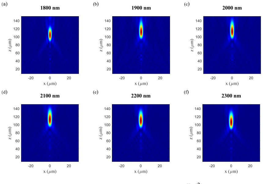
The metalens consists of periodically arranged silicon bars on CaF2 with a 900 nm period. Systematic tuning of bar length and width achieves simultaneous dispersion compensation and phase modulation. FDTD simulations confirm suppression of chromatic aberration from 1800 to 2300 nm, with focal-length variation within 6% of the target, and show weak wavelength dependence in the degree of polarization at the focus.
What carries the argument
Silicon bar nanocell structures periodically arranged at 900 nm pitch that control local phase and group delay through length and width tuning.
Load-bearing premise
FDTD simulations accurately predict the optical performance of a real fabricated device without major losses or manufacturing deviations.
What would settle it
Fabricate the metalens and measure focal length at several wavelengths from 1800 to 2300 nm to check whether variation stays within 6 percent of the design value.
Figures


read the original abstract
The 1.8-2.3 {\mu}m band lies within the short-wavelength infrared (SWIR) region and serves as a key window for a wide range of applications, including quantum sensing, molecular spectroscopy, and free-space quantum and classical optical communication. Despite its significance, optical devices operating in this band still face two major challenges: chromatic aberration across the spectral range and difficulty of integration due to bulky optical elements. Metalenses are composed of subwavelength nanostructures that locally control the phase and group delay of light, enabling wavefront shaping and broadband dispersion compensation. These capabilities make them promising for infrared optical systems, particularly in focusing and imaging for compact devices. In this study, we propose a metalens design based on a CaF$_2$ substrate, where each nanocell consists of a silicon bar structure. These nanocells are periodically arranged with a 900~nm period, enabling control of dispersion and phase. By systematically finetuning the bar length and width, the design enables simultaneous dispersion compensation and phase modulation, achieving stable focusing performance over a broad spectral range. Finite-Difference Time-Domain (FDTD) simulations demonstrate effective suppression of chromatic aberration across 1800 - 2300 nm, with focal-length variation within 6% of the target value. We further analyze the polarization distribution across the focal spot and find a weak wavelength dependence of the degree of polarization (DoP), which we attribute to the spatially varying polarization state in the high-NA focal region together with the wavelength-dependent anisotropic response of the nanostructures. This design offers a compact, broadband, and high-performance approach for beam collimation and wavefront shaping in the SWIR band, showing promising potential for quantum communication and sensing systems.
Editorial analysis
A structured set of objections, weighed in public.
Referee Report
Summary. The paper proposes a broadband achromatic metalens for the 1.8-2.3 μm SWIR band using silicon bar nanostructures on a CaF2 substrate arranged in a 900 nm periodic lattice. Systematic tuning of bar length and width is claimed to enable simultaneous phase modulation and dispersion compensation. FDTD simulations are presented to show focal-length variation within 6% of the target across the band, with additional analysis of polarization distribution at the focus indicating weak wavelength dependence in the degree of polarization.
Significance. If the reported focal-length stability holds under realistic conditions, the design would represent a compact, integrable solution for achromatic focusing in SWIR applications such as quantum sensing and free-space communication. The geometric tuning approach for dispersion engineering is a standard technique in metalens literature, but the absence of efficiency metrics, fabrication tolerance analysis, and experimental validation limits the immediate significance of the result.
major comments (3)
- [Abstract] Abstract and simulation description: The central claim of focal-length variation within 6% across 1800-2300 nm rests on FDTD results, yet no parameters are provided for mesh resolution, boundary conditions, material dispersion models (silicon and CaF2), or convergence checks. Without these, it is impossible to assess whether the dispersion compensation is accurately captured or numerically converged.
- [Results] Results section: No robustness analysis against fabrication variations (e.g., ±5-10 nm errors in bar length/width) is included. Such dimensional tolerances are typical in electron-beam or optical lithography and would simultaneously perturb both the required phase profile and group delay, potentially increasing focal-length variation beyond the stated 6% under the local-periodic approximation used for the meta-atom library.
- [Results] Performance evaluation: Focusing efficiency, transmission, and reflection losses are not reported across the band. These quantities are load-bearing for practical utility in quantum communication systems and cannot be inferred from focal-length stability alone.
minor comments (1)
- [Abstract] The abstract states the period as '900~nm'; clarify whether this is an exact design value or an approximation, and ensure consistent notation in the main text.
Simulated Author's Rebuttal
We thank the referee for the constructive and detailed comments, which have helped us improve the clarity and completeness of the manuscript. We address each major comment point by point below, providing additional information where available from our simulations and indicating revisions made to the manuscript.
read point-by-point responses
-
Referee: [Abstract] Abstract and simulation description: The central claim of focal-length variation within 6% across 1800-2300 nm rests on FDTD results, yet no parameters are provided for mesh resolution, boundary conditions, material dispersion models (silicon and CaF2), or convergence checks. Without these, it is impossible to assess whether the dispersion compensation is accurately captured or numerically converged.
Authors: We agree that explicit documentation of the FDTD parameters is required for reproducibility and to confirm numerical convergence. In the revised manuscript we have added a dedicated Numerical Methods subsection that specifies a nonuniform mesh with 5 nm resolution inside the silicon bars and 10 nm in the surrounding regions, 12-layer PML boundaries on all sides, silicon refractive index from tabulated data, CaF2 dispersion via the Sellmeier equation, and convergence tests in which halving the mesh size altered the reported focal-length variation by less than 0.5%. revision: yes
-
Referee: [Results] Results section: No robustness analysis against fabrication variations (e.g., ±5-10 nm errors in bar length/width) is included. Such dimensional tolerances are typical in electron-beam or optical lithography and would simultaneously perturb both the required phase profile and group delay, potentially increasing focal-length variation beyond the stated 6% under the local-periodic approximation used for the meta-atom library.
Authors: The referee is correct that fabrication tolerance is a practical concern not addressed in the original submission. While the manuscript centers on the ideal design under the local-periodic approximation, we have now performed additional FDTD runs with uniform ±5 nm and ±10 nm perturbations applied to all bar dimensions. These show the focal-length variation rising to approximately 8% and 13%, respectively. A concise discussion of these results together with a supplementary figure has been added to the revised manuscript. revision: yes
-
Referee: [Results] Performance evaluation: Focusing efficiency, transmission, and reflection losses are not reported across the band. These quantities are load-bearing for practical utility in quantum communication systems and cannot be inferred from focal-length stability alone.
Authors: We concur that efficiency and loss figures are essential for assessing utility. In the revised manuscript we now report the focusing efficiency (power within a 3λ-radius circle at the focal plane divided by incident power), which remains between 62% and 68% across 1800–2300 nm, average transmission above 82%, and reflection below 9%. These quantities are extracted directly from the same FDTD simulations used for the focal-length analysis and are presented in a new figure and accompanying text in the Results section. revision: yes
Circularity Check
No circularity: design tuning followed by direct FDTD verification of focal stability
full rationale
The paper's chain consists of selecting a silicon-bar meta-atom on CaF2, periodically arranging cells at 900 nm pitch, and systematically varying bar length and width to obtain simultaneous phase and group-delay control; FDTD is then run on the resulting geometry to report focal-length variation within 6 % across 1800-2300 nm. These steps are forward numerical evaluation of an explicitly constructed structure rather than any reduction of a claimed prediction to a fitted parameter, self-defined quantity, or load-bearing self-citation. No equations are presented that equate an output to an input by algebraic identity, and the performance metric is obtained from simulation of the tuned geometry itself.
Axiom & Free-Parameter Ledger
free parameters (1)
- silicon bar length and width
axioms (1)
- standard math Maxwell's equations and material dispersion relations govern light propagation through subwavelength silicon structures on CaF2
Lean theorems connected to this paper
-
IndisputableMonolith/Cost/FunctionalEquation.leanwashburn_uniqueness_aczel unclear?
unclearRelation between the paper passage and the cited Recognition theorem.
By systematically finetuning the bar length and width, the design enables simultaneous dispersion compensation and phase modulation... FDTD simulations demonstrate effective suppression of chromatic aberration across 1800-2300 nm, with focal-length variation within 6% of the target value.
-
IndisputableMonolith/Foundation/AlphaCoordinateFixation.leancostAlphaLog_high_calibrated_iff unclear?
unclearRelation between the paper passage and the cited Recognition theorem.
The phase compensation relationship... Δϕ(R,λ) = -[2π(√(R²+f²)-f)](1/λ - 1/λmax) + C(λ)
What do these tags mean?
- matches
- The paper's claim is directly supported by a theorem in the formal canon.
- supports
- The theorem supports part of the paper's argument, but the paper may add assumptions or extra steps.
- extends
- The paper goes beyond the formal theorem; the theorem is a base layer rather than the whole result.
- uses
- The paper appears to rely on the theorem as machinery.
- contradicts
- The paper's claim conflicts with a theorem or certificate in the canon.
- unclear
- Pith found a possible connection, but the passage is too broad, indirect, or ambiguous to say the theorem truly supports the claim.
Reference graph
Works this paper leans on
-
[1]
J. C. Mars and L. C. Rowan, “Spectral assessment of new aster swir surface reflectance data products for spectroscopic mapping of rocks and minerals,” Remote. Sens. Environ.114, 2011– 2025 (2010)
work page 2011
-
[2]
A. Campargue, S. N. Mikhailenko, S. Vasilchenko, C. Reynaud, S. B ´eguier, P. ˇCerm´ak, D. Mon- delain, S. Kassi, and D. Romanini, “The absorption spectrum of water vapor in the 2.2µm trans- parency window: High sensitivity measurements and spectroscopic database,” J. Quant. Spectrosc. Radiat. Transf.189, 407–416 (2017)
work page 2017
-
[3]
Revisiting short-wave- infrared (swir) bands for atmospheric correction in coastal waters,
N. Pahlevan, J. claude Roger, Z. Ahmad, H. R. Gordon, and M. Wang, “Revisiting short-wave- infrared (swir) bands for atmospheric correction in coastal waters,” Opt. Express, V ol. 25, Issue 6, pp. 6015-603525, 6015–6035 (2017)
work page 2017
-
[4]
A swir based algorithm to retrieve total suspended matter in extremely turbid waters,
E. Knaeps, K. G. Ruddick, D. Doxaran, A. I. Dogliotti, B. Nechad, D. Raymaekers, and S. Sterckx, “A swir based algorithm to retrieve total suspended matter in extremely turbid waters,” Remote. Sens. Environ.168, 66–79 (2015)
work page 2015
-
[5]
Swir digital holography and imag- ing through smoke and flames: unveiling the invisible,
E. Pugliese, M. Locatelli, R. Meucci, S. Euzzor, and P. Poggi, “Swir digital holography and imag- ing through smoke and flames: unveiling the invisible,” Opt. Express, V ol. 31, Issue 25, pp. 42090- 4209831, 42090–42098 (2023)
work page 2023
-
[6]
Short wave infrared (swir) imaging systems using small unmanned aerial systems (suas),
B. Stark, M. McGee, and Y . Chen, “Short wave infrared (swir) imaging systems using small unmanned aerial systems (suas),” 2015 Int. Conf. on Unmanned Aircr. Syst. ICUAS 2015 pp. 495–501 (2015)
work page 2015
-
[7]
All-weather drone vision: Passive swir imaging in fog and rain,
A. Bessonov, A. Rozanov, R. White, G. Suwito, I. Medina-Salazar, M. Lutfullin, D. Gusev, and I. Shikov, “All-weather drone vision: Passive swir imaging in fog and rain,” Drones 2025, V ol. 9, Page 5539, 553 (2025)
work page 2025
-
[8]
High-sensitivity short-wave infrared technology for thermal imaging,
M. Wen, L. Wei, X. Zhuang, D. He, S. Wang, and Y . Wang, “High-sensitivity short-wave infrared technology for thermal imaging,” Infrared Phys. & Technol.95, 93–99 (2018)
work page 2018
-
[9]
Extended short-wave infrared absorption in group iv nanowire arrays,
A. Attiaoui, ´E. Bouthillier, G. Daligou, A. Kumar, S. Assali, and O. Moutanabbir, “Extended short-wave infrared absorption in group iv nanowire arrays,” Phys. Rev. Appl.15(2020)
work page 2020
-
[10]
S. Sarkar, P. Le, J. Geng, Y . Liu, Z. Han, M. U. Zahid, D. Nall, Y . Youn, P. R. Selvin, and A. M. Smith, “Short-wave infrared quantum dots with compact sizes as molecular probes for fluores- cence microscopy,” J. Am. Chem. Soc.142, 3449 (2020)
work page 2020
-
[11]
Colloidal iii–v quantum dot photodiodes for short-wave infrared photodetection,
J. Leemans, V . P. Pejovi ´c, E. Georgitzikis, M. Minjauw, A. B. Siddik, Y .-H. Deng, Y . Kuang, G. Roelkens, C. Detavernier, I. Lieberman, P. E. Malinowski, D. Cheyns, Z. Hens, J. Leemans, Y .-H. Deng, Z. Hens, V . P. Pejovi´c, E. Georgitzikis, A. B. Siddik, Y . Kuang, I. Lieberman, P. E. Malinowski, D. Cheyns, M. Minjauw, C. Detavernier, and G. Roelkens...
work page 2022
-
[12]
R. H. Wilson, K. P. Nadeau, F. B. Jaworski, B. J. Tromberg, and A. J. Durkin, “Review of short-wave infrared spectroscopy and imaging methods for biological tissue characterization,” J. Biomed. Opt.20, 030901 (2015)
work page 2015
-
[13]
Rotating mirror short-wave infrared hyperspectral imaging system: Characterization and applications,
J. A. Guti ´errez-Guti´errez, V . Mieites, J. M. L´opez-Higuera, and O. M. Conde, “Rotating mirror short-wave infrared hyperspectral imaging system: Characterization and applications,” Sensors Actuators B: Chem.439, 137762 (2025)
work page 2025
-
[14]
A knowledge-based strategy for interpretation of swir hyperspectral images of rocks,
F. J. A. van Ruitenbeek, W. H. Bakker, H. M. A. van der Werff, C. A. Hecker, K. A. A. Hein, and W. van Eijndthoven, “A knowledge-based strategy for interpretation of swir hyperspectral images of rocks,” Remote. Sens. 2025, V ol. 17, Page 255517, 2555 (2025)
work page 2025
-
[15]
Detection and identification of plastics using swir hyperspectral imaging,
M. Mehrubeoglu, A. V . Sickle, and J. Turner, “Detection and identification of plastics using swir hyperspectral imaging,” (SPIE-Intl Soc Optical Eng, 2020), p. 15
work page 2020
-
[16]
B. Keizers, T. S. Nijboer, C. A. M. van der Fels, M. C. van den Heuvel, G. M. van Dam, S. Krui- jff, I. J. de Jong, M. J. H. Witjes, F. J. V oskuil, D. Gorpas, W. R. Browne, and P. J. van der Zaag, “Systematic comparison of fluorescence imaging in the near-infrared and shortwave-infrared spec- tral range using clinical tumor samples containing cetuximab-i...
work page 2024
-
[17]
A stable and biocompatible short- wave infrared nanoribbon for dual-channel in vivo imaging,
C. Yao, R. Wei, X. Luo, J. Zhou, X. Zhang, X. Lu, Y . Dong, R. Chu, Y . Sun, Y . Wang, W. Xia, D. Qu, C. Liu, J. Ren, G. Ge, J. Chen, X. Qian, and Y . Yang, “A stable and biocompatible short- wave infrared nanoribbon for dual-channel in vivo imaging,” Nat. Commun.16, 1–12 (2025)
work page 2025
-
[18]
M. Abuzar, K. Sheffield, and A. McAllister, “Feasibility of using swir-transformed reflectance (str) in place of surface temperature (ts) for the mapping of irrigated landcover,” Land 2024, V ol. 13, Page 63313, 633 (2024)
work page 2024
-
[19]
C. W. Golden, R. Griffin, W. Schroder, K. Herndon, J. Casana, and C. Ferwerda, “Drone-acquired short-wave infrared (swir) imagery in landscape archaeology: An experimental approach,” Re- mote. Sens. 2024, V ol. 16, Page 167116, 1671 (2024)
work page 2024
-
[20]
S. L. Ustin and E. M. P. Middleton, “Current and near-term earth-observing environmental satel- lites, their missions, characteristics, instruments, and applications,” Sensors (Basel, Switzerland) 24, 3488 (2024)
work page 2024
-
[21]
D. J. Jacob, D. J. Varon, D. H. Cusworth, P. E. Dennison, C. Frankenberg, R. Gautam, L. Guanter, J. Kelley, J. McKeever, L. E. Ott, B. Poulter, Z. Qu, A. K. Thorpe, J. R. Worden, and R. M. Duren, “Quantifying methane emissions from the global scale down to point sources using satellite observations of atmospheric methane,” Atmospheric Chem. Phys.22, 9617–...
work page 2022
-
[22]
C-red 3: A swir camera for fso applications,
J. L. Gach, D. Boutolleau, C. Brun, T. Carmignani, F. Clop, P. Feautrier, S. Lemarchand, E. Stadler, and Y . Wanwanscappel, “C-red 3: A swir camera for fso applications,” (2020)
work page 2020
-
[23]
Wavelength selection for satellite quantum key distribution,
S. Hearne, J. Horgan, N. Boujnah, and D. Kilbane, “Wavelength selection for satellite quantum key distribution,” Appl. Sci. 2025, V ol. 15, Page 130815, 1308 (2025)
work page 2025
-
[24]
Two-photon quantum interference and entanglement at 2.1µm,
S. Prabhakar, T. Shields, A. C. Dada, M. Ebrahim, G. G. Taylor, D. Morozov, K. Erotokritou, S. Miki, M. Yabuno, H. Terai, C. Gawith, M. Kues, L. Caspani, R. H. Hadfield, and M. Clerici, “Two-photon quantum interference and entanglement at 2.1µm,” Sci. Adv.6, 5195–5222 (2020)
work page 2020
-
[25]
Recent advances on integrated quantum communications,
A. Orieux and E. Diamanti, “Recent advances on integrated quantum communications,” J. Opt. 18, 083002 (2016)
work page 2016
-
[26]
Ad- vances in quantum cryptography,
S. Pirandola, S. Pirandola, U. L. Andersen, L. Banchi, M. Berta, D. Bunandar, R. Colbeck, D. En- glund, T. Gehring, C. Lupo, C. Ottaviani, J. L. Pereira, M. Razavi, J. S. Shaari, J. S. Shaari, M. Tomamichel, M. Tomamichel, V . C. Usenko, G. Vallone, P. Villoresi, and P. Wallden, “Ad- vances in quantum cryptography,” Adv. Opt. Photonics, V ol. 12, Issue 4,...
work page 2020
-
[27]
Enhanced swir photodetection in colloidal quantum dot photodiodes via tunneling current suppression,
H. C. V . Tran, E. Jang, J. Kim, M. Choi, Y . Park, H. Jeong, T. Goo, S. Bae, and S. Jeong, “Enhanced swir photodetection in colloidal quantum dot photodiodes via tunneling current suppression,” ACS Appl. Mater. & Interfaces17, 15666–15674 (2025)
work page 2025
-
[28]
Recent advances in infrared imagers: Toward thermodynamic and quantum limits of photon sensitivity,
S. Bianconi and H. Mohseni, “Recent advances in infrared imagers: Toward thermodynamic and quantum limits of photon sensitivity,” Reports on progress physics. Phys. Soc. (Great Britain)83, 044101 (2020)
work page 2020
-
[29]
Metalenses: Versatile multifunctional photonic components,
M. Khorasaninejad and F. Capasso, “Metalenses: Versatile multifunctional photonic components,” Science358(2017)
work page 2017
-
[30]
A. Arbabi, Y . Horie, M. Bagheri, and A. Faraon, “Dielectric metasurfaces for complete control of phase and polarization with subwavelength spatial resolution and high transmission,” Nat. Nan- otechnol.10, 937–943 (2015)
work page 2015
-
[31]
Ultrahigh numerical aperture metalens at visible wavelengths,
H. Liang, Q. Lin, X. Xie, Q. Sun, Y . Wang, L. Zhou, L. Liu, X. Yu, J. Zhou, T. F. Krauss, and J. Li, “Ultrahigh numerical aperture metalens at visible wavelengths,” Nano Lett.18, 4460–4466 (2018)
work page 2018
-
[32]
Long wavelength infrared imaging under ambient thermal radiation via an all-silicon metalens,
L. Huang, Z. Coppens, K. Hallman, Z. Han, K. F. B ¨ohringer, N. Akozbek, A. Raman, A. Ma- jumdar, and A. Majumdar, “Long wavelength infrared imaging under ambient thermal radiation via an all-silicon metalens,” Opt. Mater. Express, V ol. 11, Issue 9, pp. 2907-291411, 2907–2914 (2021)
work page 2021
-
[33]
Gan metalens for pixel-level full-color routing at visible light,
B. H. Chen, P. C. Wu, V . C. Su, Y . C. Lai, C. H. Chu, I. C. Lee, J. W. Chen, Y . H. Chen, Y . C. Lan, C. H. Kuan, and D. P. Tsai, “Gan metalens for pixel-level full-color routing at visible light,” Nano Lett.17, 6345–6352 (2017)
work page 2017
-
[34]
Dual-polarity plasmonic metalens for visible light,
X. Chen, L. Huang, H. M ¨uhlenbernd, G. Li, B. Bai, Q. Tan, G. Jin, C. W. Qiu, S. Zhang, and T. Zentgraf, “Dual-polarity plasmonic metalens for visible light,” Nat. Commun.3, 1–6 (2012)
work page 2012
-
[35]
Plasmonics metalens independent from the incident polarizations,
W. Wang, Z. Guo, R. Li, J. Zhang, Y . Li, Y . Liu, X. Wang, S. Qu, L. Verslegers, P. B. Catrysse, Z. Yu, J. S. White, E. S. Barnard, M. L. Brongersma, S. Fan, H. Gao, J. K. Hyun, M. H. Lee, J. C. Yang, L. J. Lauhon, and T. W. Odom, “Plasmonics metalens independent from the incident polarizations,” Opt. Express, V ol. 23, Issue 13, pp. 16782-1679123, 16782...
work page 2015
-
[36]
An achromatic metalens in the near-infrared region with an array based on a single nano-rod unit,
B. Yu, J. Wen, X. Chen, and D. Zhang, “An achromatic metalens in the near-infrared region with an array based on a single nano-rod unit,” Appl. Phys. Express12, 092003 (2019)
work page 2019
-
[37]
Polarization controlled dual functional reflective planar metalens in near infrared regime,
Y . Zhang, B. Yang, Z. Liu, and Y . Fu, “Polarization controlled dual functional reflective planar metalens in near infrared regime,” Coatings 2020, V ol. 10, Page 38910, 389 (2020)
work page 2020
-
[38]
S. Xiao, S. Xiao, F. Zhao, D. Wang, J. Weng, J. Weng, Y . Wang, X. He, H. Chen, Z. Zhang, Y . Yu, Z. Zhang, Z. Zhang, Z. Zhang, Z. Zhang, J. Yang, and J. Yang, “Inverse design of a near- infrared metalens with an extended depth of focus based on double-process genetic algorithm optimization,” Opt. Express, V ol. 31, Issue 5, pp. 8668-868131, 8668–8681 (2023)
work page 2023
-
[39]
Y . Zou, Y . Xu, and M. Fang, “Broadband polarisation-insensitive metalens design with easy func- tionality expansion on an ingaas-detector substrate off-chip,” SSRN Prepr. p. ssrn.5221467 (2025)
work page 2025
-
[40]
S. Zhang, M. hwan Kim, F. Aieta, A. She, T. Mansuripur, I. Gabay, M. Khorasaninejad, D. Rousso, X. Wang, M. Troccoli, F. Capasso, N. Yu, P. Genevet, F. Aieta, M. A. Kats, R. Blanchard, G. Aoust, J. P. Tetienne, Z. Gaburro, F. Capasso, A. Kats, M. Khorasaninejad, W. T. Chen, R. C. Devlin, J. Oh, and A. Y . Zhu, “High efficiency near diffraction-limited mid...
work page 2016
-
[41]
Mid-infrared polarization devices based on the double-phase modulating dielectric metasurface,
Z. Guo, L. Tian, F. Shen, H. Zhou, and K. Guo, “Mid-infrared polarization devices based on the double-phase modulating dielectric metasurface,” J. Phys. D: Appl. Phys.50, 254001 (2017)
work page 2017
-
[42]
Mid-infrared polarization-controlled broadband achromatic metadevice,
K. Ou, F. Yu, G. Li, W. Wang, A. E. Miroshnichenko, L. Huang, P. Wang, T. Li, Z. Li, X. Chen, and W. Lu, “Mid-infrared polarization-controlled broadband achromatic metadevice,” Sci. Adv. 6, 711–722 (2020)
work page 2020
-
[43]
S. Yue, S. Yue, S. Yue, Y . Liu, Y . Liu, R. Wang, R. Wang, Y . Hou, Y . Hou, H. Shi, H. Shi, Y . Feng, Y . Feng, Z. Wen, Z. Wen, Z. Zhang, and Z. Zhang, “All-silicon polarization-independent broadband achromatic metalens designed for the mid-wave and long-wave infrared,” Opt. Express, V ol. 31, Issue 26, pp. 44340-4435231, 44340–44352 (2023)
work page 2023
-
[44]
Inverse design broadband achromatic and polarizations-insensitive metalens in mid-infrared,
S. Xu, P. Kang, J. Chen, Z. Hu, W. Chang, and F. Huang, “Inverse design broadband achromatic and polarizations-insensitive metalens in mid-infrared,” Opt. Commun.579, 131586 (2025)
work page 2025
-
[45]
Telecom-band high contrast narrowband metalens for 3d imag- ing,
K. Liu, C. Sun, and H. C. Chui, “Telecom-band high contrast narrowband metalens for 3d imag- ing,” Opt. Lasers Eng.180, 108325 (2024)
work page 2024
-
[46]
Dispersion- engineered spin photonics based on folded-path metasurfaces,
F. Zhang, H. Bao, M. Pu, Y . Guo, T. Kang, X. Li, Q. He, M. Xu, X. Ma, and X. Luo, “Dispersion- engineered spin photonics based on folded-path metasurfaces,” Light. Sci. Appl.14, 1–10 (2025)
work page 2025
-
[48]
High-efficiency broadband achromatic metalens for near-ir biological imaging window,
Y . Wang, Q. Chen, W. Yang, Z. Ji, L. Jin, X. Ma, Q. Song, A. Boltasseva, J. Han, V . M. Sha- laev, and S. Xiao, “High-efficiency broadband achromatic metalens for near-ir biological imaging window,” Nat. Commun.12, 1–7 (2021)
work page 2021
-
[49]
A broad- band achromatic metalens for focusing and imaging in the visible,
W. T. Chen, A. Y . Zhu, V . Sanjeev, M. Khorasaninejad, Z. Shi, E. Lee, and F. Capasso, “A broad- band achromatic metalens for focusing and imaging in the visible,” Nat. Nanotechnol.13, 220–226 (2018)
work page 2018
-
[50]
Multiwavelength achromatic metasurfaces by dispersive phase compensation,
F. Aieta, M. A. Kats, P. Genevet, and F. Capasso, “Multiwavelength achromatic metasurfaces by dispersive phase compensation,” Science347, 1342–1345 (2015)
work page 2015
-
[51]
A broadband achromatic metalens in the visible,
S. Wang, P. C. Wu, V . C. Su, Y . C. Lai, M. K. Chen, H. Y . Kuo, B. H. Chen, Y . H. Chen, T. T. Huang, J. H. Wang, R. M. Lin, C. H. Kuan, T. Li, Z. Wang, S. Zhu, and D. P. Tsai, “A broadband achromatic metalens in the visible,” Nat. Nanotechnol.13, 227–232 (2018)
work page 2018
-
[52]
Broadband achromatic metalens with polar- ization insensitivity in the mid-infrared range,
K. Guo, C. Wang, Q. Kang, L. Chen, and Z. Guo, “Broadband achromatic metalens with polar- ization insensitivity in the mid-infrared range,” Opt. Mater.131, 112489 (2022)
work page 2022
-
[53]
On-chip integration of achromatic metalens arrays,
Y . Zhang, X. Jiang, G. Qu, J. Han, C. Li, B. Bo, Q. Ruan, Z. Liu, Q. Song, and S. Xiao, “On-chip integration of achromatic metalens arrays,” Nat. Commun.16, 1–8 (2025)
work page 2025
-
[54]
A broadband achromatic polarization-insensitive metalens consisting of anisotropic nanostructures,
W. T. Chen, A. Y . Zhu, J. Sisler, Z. Bharwani, and F. Capasso, “A broadband achromatic polarization-insensitive metalens consisting of anisotropic nanostructures,” Nat. Commun.10, 1– 7 (2019)
work page 2019
-
[55]
V . R. Manfrinato, J. Wen, L. Zhang, Y . Yang, R. G. Hobbs, B. Baker, D. Su, D. Zakharov, N. J. Za- luzec, D. J. Miller, E. A. Stach, and K. K. Berggren, “Determining the resolution limits of electron- beam lithography: Direct measurement of the point-spread function,” Nano Lett.14, 4406–4412 (2014)
work page 2014
-
[56]
A novel fabrication technique for high-aspect-ratio nanopillar arrays for sers application,
T. Duan, C. Gu, D. S. Ang, K. Xu, and Z. Liu, “A novel fabrication technique for high-aspect-ratio nanopillar arrays for sers application,” RSC Adv.10, 45037–45041 (2020)
work page 2020
-
[57]
Fabrication of ultrahigh aspect ratio si nanopillar and nanocone arrays,
A. Pan, M. Samaan, Z. Yan, W. Hu, B. Cui, J. B. V . S. Technol, and B. C. AFFILIATIONS, “Fabrication of ultrahigh aspect ratio si nanopillar and nanocone arrays,” J. Vac. Sci. & Technol. B41, 23001 (2023)
work page 2023
-
[58]
Q. Song, J. Cai, C. Wang, L. Zhou, Y . Chen, M. Zhou, J. Zhang, B. Yang, Y . Yang, A. Yi, T. You, and X. Ou, “Wafer-scale fabrication of single-crystalline calcium fluoride thin-film on insulator by ion-cutting,” Opt. Mater.157, 115787 (2024)
work page 2024
-
[59]
Robustness analysis of metasurfaces: Perfect struc- tures are not always the best,
H. C. Wang, K. Achouri, and O. J. Martin, “Robustness analysis of metasurfaces: Perfect struc- tures are not always the best,” ACS Photonics9, 2438–2447 (2022)
work page 2022
-
[60]
The effect of height error on performance of propagation phase-based metalens,
Y . Qiu, L. Deng, Y . Zhan, G. Li, and J. Guan, “The effect of height error on performance of propagation phase-based metalens,” Micromachines 2024, V ol. 15, Page 54015, 540 (2024)
work page 2024
discussion (0)
Sign in with ORCID, Apple, or X to comment. Anyone can read and Pith papers without signing in.