REVIEW 4 major objections 5 minor 39 references
Multiport Analytical Pixel Electromagnetic Simulator (MAPES) for AI-assisted RFIC and Microwave Circuit Design
T0 review · 4 major / 5 minor · reviewed 2026-08-03 · deepseek-v4-flash
Pith's one-line read Closed-form matrix equation predicts any pixel layout's EM response.
desk verdict MAPES is a legitimate, well-motivated physics-based surrogate for pixel-based RFIC/PCB design, but the 'any arbitrary pattern' claim outruns the evidence: five random patterns per case and an empirical equivalence assumption that needs broader validation. read the letter →
The pith
A machine-rendered reading of the paper's core claim, the machinery that carries it, and where it could break.
The reading
What carries the argument
The carrying mechanism is the replacement of the seamless pixel array by an equivalent multiport network. Each original pixel becomes a slightly smaller virtual pixel, and small diagonal virtual pixels are placed at the corners; virtual ports are inserted between adjacent virtual pixels, between virtual pixels and diagonal virtual pixels, and between pixels and ground, plus optional inter-layer via ports. The impedance matrix Z_ALL of this network is extracted once with Q full-wave port excitations. A pixel pattern P is then converted by a deterministic algorithm into a diagonal load matrix Z_L(P) of open/short terminations. Substituting into Eq. (7) yields the I/O impedance analytically. Th
What would settle it
Take a single-layer PCB pixel array with a layout that creates a narrow slot between two pixel blocks, and sweep the virtual-pixel size ratio from 70% to 95%. If the MAPES-predicted S21 resonance shifts monotonically by more than the mean error reported in Table I while the full-wave result stays fixed, the equivalence assumption is falsified.
Extended reading notes
Core claim
The central claim is Eq. (7): for any pixel pattern P, Z_MAPES(P) = Z_IO,IO − Z_IO,VP (Z_L(P) + Z_VP,VP)^−1 Z_VP,IO. Here Z_ALL is the impedance matrix among all virtual ports, obtained once from full-wave simulations of the virtual structure; Z_L(P) is a diagonal load matrix whose entries are shorts/opens determined by pixel and via presence; and the I/O ports are a subset of virtual ports. The paper argues this formula predicts the S-parameters of any layout in the design space without further full-wave simulation, because Z_ALL encodes all horizontal, vertical, diagonal, and inter-layer couplings. The formula is not a learned approximation; it follows from Kirchhoff/multiport constraints,
Load-bearing premise
The load-bearing premise is that the EM response of the mapped virtual-pixel structure (with gaps, diagonal corner pixels, and point loads) is equivalent to the original seamless pixel pattern — which requires that unconnected virtual pixels barely couple and that shrinking pixels to ~85% does not change the behavior.
Editorial extensions
If this is right
- Any pixel layout in the design space, including ones never simulated, can be evaluated in the time of one matrix inversion, so exhaustive search and inverse design become feasible.
- Only a one-time pre-simulation of Q ports (typically ~1% of a CNN training set) is needed; multi-layer and via configurations are handled by adding via ports.
- Because predictions derive from multiport theory rather than regression, MAPES avoids overfitting and gives physically consistent results across all patterns.
- MAPES can generate training datasets for AI emulators 500-2000x faster than full-wave solvers, making larger design spaces accessible.
- The closed-form structure allows low-rank/Woodbury updates when only a few pixels change, enabling fast direct-binary-search optimization.
Reading between the lines
- If the equivalence assumption holds at scale, MAPES could serve as the physics-based reward function for reinforcement-learning layout optimization, giving RL agents fast evaluation of millions of candidates.
- The 85% virtual-pixel ratio is an empirical guideline; a natural extension is to derive an optimal ratio from substrate and frequency parameters, or to use multiple virtual-pixel sizes to bound the modeling error.
- Eq. (7) suggests a hybrid approach: train a tiny neural network to predict the inverse of (Z_L+Z_VP,VP) directly, preserving exactness while matching the speed of learned surrogates.
- The method's port-count scaling may limit very large arrays; port reduction or adaptive port placement could extend it to 100x100 or larger design spaces.
Editorial analysis
A structured set of objections, weighed in public.
Referee Report
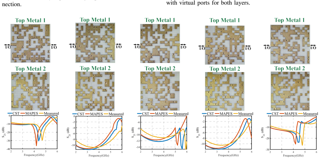
Summary. The paper proposes MAPES, an analytical multiport surrogate for pixel-based microwave/RFIC structures. A virtual-pixel equivalent model with diagonal virtual pixels is equipped with virtual ports; a one-time set of Q full-wave simulations yields an impedance matrix Z_ALL. Any pixel presence/absence pattern P is mapped to a diagonal load matrix Z_L(P), and the I/O impedance is predicted by Eq. (7): Z_MAPES(P)=Z_IO,IO−Z_IO,VP(Z_L(P)+Z_VP,VP)^−1 Z_VP,IO. The authors validate the method on four configurations (single- and double-layer PCB, 180 nm and 65 nm CMOS, the latter with vias), with five random patterns per case, reporting mean S-parameter errors of 0.016–0.220 and 615–2107× speedups over CST; PCB prototypes are also measured. The paper claims that MAPES generalizes to all pixel configurations, avoids data-driven overfitting, and requires only ~1% of the full-wave simulations of AI-based emulators.
Significance. If the equivalent-model assumption is valid for the intended design class, MAPES is a significant contribution: it replaces large data-hungry surrogates with a compact, precomputed operator and a closed-form Schur complement. The derivation of Eq. (7) is mathematically sound for the virtual-port network, and the reported CMOS agreement (mean errors 0.0164 and 0.0275) is excellent. The fabricated PCB prototypes add credibility. The method could serve as a fast physics-based simulator, a dataset generator, or a physics anchor in multi-fidelity AI design. However, the significance is conditional: the paper's broad generalization claim rests on an equivalence assumption (Sec. IV.C) that is supported only by five random validation patterns per configuration. No code or test data are provided, which would substantially aid reproducibility.
major comments (4)
- [Sec. IV.C / Fig. 18] The load-bearing assumption is stated in Sec. IV.C: the EM response of the mapped virtual-pixel structure is equivalent to that of the original seamless pixel pattern, requiring (i) negligible coupling between unconnected virtual pixels and (ii) no significant distortion from reducing virtual pixels to ~85% of the original size. Eq. (7) is exact for the virtual-port network but is not an exact statement about the original pixel geometry. The 85% ratio is an empirical guideline, not a derived quantity, and no error bounds are provided. With only random validation patterns, the equivalence is not demonstrated for long meanders, large contiguous blocks, narrow resonant traces, or systematic diagonal chains, which are precisely the structures where discrete short/open ports and a 15% size reduction are most likely to alter the electrical response. Please either expand the validation to struc
- [Sec. III / Figs. 8, 11, 14, 17; Table I] Each of the four configurations is validated with only five random pixel patterns. Random ~50%-occupancy patterns are statistically unlikely to contain long connected conductors, dense clusters, periodic via arrays, or other structured layouts common in practical microwave/RFIC passives. These are also the cases most sensitive to the equivalent-model approximation. To support the abstract's claim of 'accurate results across all design variations,' the authors should include structured test sets, report worst-case and per-pattern errors, and provide a coverage measure or error distribution. Without this, the generalization claim is anecdotal rather than demonstrated.
- [Table I / Sec. IV.A] The PCB mean S-parameter errors are 0.2199 (single-layer) and 0.1810 (double-layer). The paper attributes these to frequency shifts, but a resonance shift of even a few percent can be decisive for filter/coupler specifications, so this explanation does not make the errors negligible. Please quantify the frequency shifts, report the maximum error and the error at resonance, and clearly scope the PCB accuracy claims. As written, the statement in Sec. IV.A that these deviations are 'entirely acceptable' is not supported by the evidence.
- [Eq. (2) vs Sec. III.B] For the 13×13 two-layer CMOS 65 nm example with vias, Eq. (2) gives Q = 2(6·13·13 − 3·13 − 3·13 + 4) + 1·13·13 = 2049, but Sec. III.B reports 2013 virtual ports and 2013 CST runs. This discrepancy affects the size of Z_ALL and the pre-simulation cost. Please reconcile the formula with the example, or clarify which vias/ports are excluded.
minor comments (5)
- [Abstract / Sec. I / Sec. IV.B] The prior-data ratio is stated inconsistently: the abstract says 'about 1%', Sec. I says '2~5%', and Sec. IV.B says 'roughly equivalent to 1%'. Please unify and define the comparison basis explicitly.
- [Table II] The 'Relative Percentage' entries for MAPES rows appear to be off by orders of magnitude. For example, 1444/2^256 ≈ 1.25×10^-72%, not 1.24×10^-76%. Also, the section labels in the first column are mismatched (e.g., 'Single-Layer PCB (Section III A)' should refer to Section III.C, not III.A).
- [Abstract / Table I] The abstract states '600-2000× speed improvement', but Table I lists acceleration rates of 615×, 1615×, 1705×, and 2107×. Please align the range (e.g., '600-2100×').
- [Sec. II.C / Algorithm 1] The mapping algorithm uses 'infinite resistance' for open circuits, but the numerical implementation of Eq. (7) is not described. Please clarify whether a finite large resistance is used and how the open-circuit limit is handled in the matrix inversion.
- [Table II Note 2 / Fig. 3 caption] Typographical issues: 'large RAM menory' should be 'large RAM memory', and Fig. 3's caption says 'MAPS methodology' instead of 'MAPES methodology'.
Circularity Check
No significant circularity; Eq. (7) is a standard multiport reduction, and validation is external against CST and measurements.
full rationale
The derivation chain in MAPES is self-contained. Equation (7) is obtained by combining the full-wave-computed impedance matrix Z_ALL (Eq. 4) with the load matrix Z_L(P) (Eq. 5) and eliminating the virtual-port currents; this is an exact Schur-complement/multiport-loading result, not a fit to the reported S-parameters. Z_ALL is produced by independent full-wave simulations of the virtual-port structure, and the five random patterns per case are not used to set any entry of Z_ALL or to calibrate Eq. (7). The paper explicitly identifies its only load-bearing physical premise in Section IV.C: 'The key underlying assumption of MAPES is that the EM response of the mapped virtual pixel structure is equivalent to that of the original pixel pattern,' together with the two sub-assumptions about negligible coupling and the 85% virtual-pixel sizing guideline. That is a disclosed modeling/approximation limitation, not a circularity: the paper then checks the surrogate against CST and fabricated prototypes. The 85% ratio is empirical and admittedly so, but it is not a fitted parameter renamed as a prediction; it does not force Eq. (7) to equal the CST target by construction. The self-citations to IMPM and prior pixel-antenna work are used as background and contrast, not as the justification for Eq. (7), and no uniqueness theorem or ansatz is imported from those works to forbid alternatives. The central prediction is therefore an independently validated analytical consequence of the precomputed operator, with its main risk being the equivalence assumption's validity for pattern classes not covered by the five random examples — a correctness/generalization concern, not circular reasoning.
Assumptions & free parameters
free parameters (3)
- virtual_pixel_size_ratio =
~85% of original pixel size
- diagonal_virtual_pixel_dimensions =
1 × 3 µm in CMOS examples; unspecified for PCB cases
- via_load_impedance =
0 Ω (short) in mapping; nonzero practical resistance mentioned but not characterized
assumptions (4)
- standard math Standard multiport network theory: port voltages and currents are related by V = Z I, and loads satisfy V = −Z_L I.
- domain assumption Full-wave CST simulations of the virtual-port structure yield a complete and accurate Z_ALL.
- ad hoc to paper The EM response of the mapped virtual-pixel structure is equivalent to the original seamless pixel pattern.
- domain assumption Zero/infinite loads on virtual ports correctly represent pixel presence/absence.
invented entities (3)
-
Virtual pixels
-
Diagonal virtual pixels
-
Virtual ports
Cite this review
Pith. "Pith review of Multiport Analytical Pixel Electromagnetic Simulator (MAPES) for AI-assisted RFIC and Microwave Circuit Design." pith.science (2026). https://pith.science/paper/BYRBONVF
@misc{pith2026251121274,
  author       = {Pith},
  title        = {Pith review of: Multiport Analytical Pixel Electromagnetic Simulator (MAPES) for AI-assisted RFIC and Microwave Circuit Design},
  year         = {2026},
  howpublished = {\url{https://pith.science/paper/BYRBONVF}},
  note         = {Machine review of arXiv:2511.21274}
}
abstract
This paper proposes a novel analytical framework, denoted the Multiport Analytical Pixel Electromagnetic Simulator (MAPES). MAPES enables efficient and accurate prediction of the electromagnetic (EM) performance of arbitrary pixel-based microwave (MW) and RFIC structures. Unlike the Internal Multiport Method (IMPM), which optimizes only connecting elements within a fixed, gap-separated pixel skeleton, MAPES operates directly on the all-pixel presence/absence formulation used in recent MW/RFIC design. This is enabled by diagonal virtual pixels, an occupancy-to-load mapping, and a multi-layer/via port-level formulation that have no counterpart in IMPM. By introducing virtual pixels and diagonal virtual pixels and inserting virtual ports at critical positions, MAPES captures all horizontal, vertical, and diagonal electromagnetic couplings within a single multiport impedance matrix. Only a small set of full-wave simulations (typically about 1% of the datasets required by AI-assisted EM emulators) is needed to construct this matrix. Subsequently, any arbitrary pixel configuration can be evaluated analytically using a closed-form multiport relation without additional full-wave calculations. The proposed approach eliminates data-driven overfitting and ensures accurate results across all design variations. Using MAPES, comprehensive examples for single- and double-layer PCBs and CMOS processes (180 nm and 65 nm) confirm that high prediction accuracy with 600-2000$\times$ speed improvement is achieved compared to CST simulations. Owing to its efficiency, scalability, and reliability, MAPES provides a practical and versatile tool for AI-assisted MW circuit and RFIC design across diverse fabrication technologies.
Figures


Figures from the paper (10 more)



Reference graph
Works this paper leans on
-
[1]
A comprehensive survey on internet of things (iot) toward 5g wireless systems,
L. Chettri and R. Bera, “A comprehensive survey on internet of things (iot) toward 5g wireless systems,”IEEE Internet of Things Journal, vol. 7, no. 1, pp. 16–32, 2020
2020
-
[2]
5g: A tutorial overview of standards, trials, challenges, deployment, and practice,
M. Shafi, A. F. Molisch, P. J. Smith, T. Haustein, P. Zhu, P. De Silva, F. Tufvesson, A. Benjebbour, and G. Wunder, “5g: A tutorial overview of standards, trials, challenges, deployment, and practice,”IEEE Journal on Selected Areas in Communications, vol. 35, no. 6, pp. 1201–1221, 2017
2017
-
[3]
A vision of 6g wireless systems: Applications, trends, technologies, and open research problems,
W. Saad, M. Bennis, and M. Chen, “A vision of 6g wireless systems: Applications, trends, technologies, and open research problems,”IEEE Network, vol. 34, no. 3, pp. 134–142, 2020
2020
-
[4]
On the road to 6g: Visions, requirements, key technologies, and testbeds,
C.-X. Wang, X. You, X. Gao, X. Zhu, Z. Li, C. Zhang, H. Wang, Y . Huang, Y . Chen, H. Haas, J. S. Thompson, E. G. Larsson, M. D. Renzo, W. Tong, P. Zhu, X. Shen, H. V . Poor, and L. Hanzo, “On the road to 6g: Visions, requirements, key technologies, and testbeds,”IEEE Communications Surveys & Tutorials, vol. 25, no. 2, pp. 905–974, 2023
2023
-
[5]
Deep-learning-based inverse- designed millimeter-wave passives and power amplifiers,
E. A. Karahan, Z. Liu, and K. Sengupta, “Deep-learning-based inverse- designed millimeter-wave passives and power amplifiers,”IEEE Journal of Solid-State Circuits, vol. 58, no. 11, pp. 3074–3088, 2023
2023
-
[6]
Design of highly efficient broadband class-e power amplifier using synthesized low-pass matching networks,
K. Chen and D. Peroulis, “Design of highly efficient broadband class-e power amplifier using synthesized low-pass matching networks,”IEEE Transactions on Microwave Theory and Techniques, vol. 59, no. 12, pp. 3162–3173, 2011
2011
-
[7]
A robust high-q micromachined rf inductor for rfic applications,
J.-W. Lin, C. Chen, and Y .-T. Cheng, “A robust high-q micromachined rf inductor for rfic applications,”IEEE Transactions on Electron Devices, vol. 52, no. 7, pp. 1489–1496, 2005. IEEE 18
2005
-
[8]
An n-way hybrid power divider,
E. Wilkinson, “An n-way hybrid power divider,”IRE Transactions on Microwave Theory and Techniques, vol. 8, no. 1, pp. 116–118, 1960
1960
Show all 39 references
-
[9]
On-chip spiral inductors with patterned ground shields for si-based rf ics,
C. Yue and S. Wong, “On-chip spiral inductors with patterned ground shields for si-based rf ics,”IEEE Journal of Solid-State Circuits, vol. 33, no. 5, pp. 743–752, 1998
1998
-
[10]
Deep learning-assisted rfic design with dual-metal-layer passive matching networks: A 15-22 ghz cmos pa for 6g in 22nm fdx+,
C. Chu, E. Liu, Y . Liu, B. Lin, M. Eleraky, B. Abdelaziz, M. Ghor- banpoor, T.-Y . Huang, A. Wang, and H. Wang, “Deep learning-assisted rfic design with dual-metal-layer passive matching networks: A 15-22 ghz cmos pa for 6g in 22nm fdx+,” in2025 16th German Microwave Conferen...
2025
-
[11]
Ai-assisted template-seeded pixelated design for multi-metal-layer high-coupling em structures: A ku-band 6g fr3 pa in 22nm fdx+,
C. Chu, J. Xu, Y . Liu, J. Zeng, A. Wang, T. Torii, S. Shinjo, K. Ya- manaka, and H. Wang, “Ai-assisted template-seeded pixelated design for multi-metal-layer high-coupling em structures: A ku-band 6g fr3 pa in 22nm fdx+,” in2025 IEEE/MTT-S International Microwave Symposium - ...
2025
-
[12]
Dall-em: Generative ai with diffusion models for new design space discovery and target-to-electromagnetic structure synthesis,
Y . Guo, E. A. Karahan, Z. Li, Z. Shao, Z. Zhang, M. Wang, and K. Sen- gupta, “Dall-em: Generative ai with diffusion models for new design space discovery and target-to-electromagnetic structure synthesis,” in 2025 IEEE/MTT-S International Microwave Symposium - IMS 2025, 2025,...
2025
-
[13]
Ims deep learning enabled generalized synthesis of multi-port electromagnetic structures and cir- cuits for mmwave power amplifiers,
E. A. Karahan, Z. Liu, and K. Sengupta, “Ims deep learning enabled generalized synthesis of multi-port electromagnetic structures and cir- cuits for mmwave power amplifiers,” in2024 IEEE/MTT-S International Microwave Symposium - IMS 2024, 2024, pp. 184–187
2024
-
[14]
Deep-learning enabled generalized inverse design of multi-port radio-frequency and sub-terahertz passives and integrated circuits,
E. A. Karahan, Z. Liu, A. Gupta, Z. Shao, J. Zhou, U. Khankhoje, and K. Sengupta, “Deep-learning enabled generalized inverse design of multi-port radio-frequency and sub-terahertz passives and integrated circuits,”Nature communications, vol. 15, no. 1, p. 10734, 2024
2024
-
[15]
Algorithmic design and optimization of on-chip multilayered pixelated passive networks,
V . Chenna and H. Hashemi, “Algorithmic design and optimization of on-chip multilayered pixelated passive networks,”IEEE Transactions on Microwave Theory and Techniques, pp. 1–11, 2025
2025
-
[16]
Tandem neural network based design of multiband antennas,
A. Gupta, E. A. Karahan, C. Bhat, K. Sengupta, and U. K. Khankhoje, “Tandem neural network based design of multiband antennas,”IEEE Transactions on Antennas and Propagation, vol. 71, no. 8, pp. 6308– 6317, 2023
2023
-
[17]
Goodfellow, Y
I. Goodfellow, Y . Bengio, A. Courville, and Y . Bengio,Deep learning. MIT press Cambridge, 2016, vol. 1, no. 2
2016
-
[18]
Dropout: a simple way to prevent neural networks from over- fitting,
N. Srivastava, G. Hinton, A. Krizhevsky, I. Sutskever, and R. Salakhut- dinov, “Dropout: a simple way to prevent neural networks from over- fitting,”The journal of machine learning research, vol. 15, no. 1, pp. 1929–1958, 2014
1929
-
[19]
A compact antenna reconfigurable in the band 1.7ghz - 2.7ghz,
J. Araque and G. Vecchi, “A compact antenna reconfigurable in the band 1.7ghz - 2.7ghz,” in2006 IEEE Antennas and Propagation Society International Symposium, 2006, pp. 2333–2336
2006
-
[20]
An efficient approach for optimizing frequency reconfigurable pixel antennas using genetic algorithms,
S. Song and R. D. Murch, “An efficient approach for optimizing frequency reconfigurable pixel antennas using genetic algorithms,”IEEE Transactions on Antennas and Propagation, vol. 62, no. 2, pp. 609–620, 2014
2014
-
[21]
Multiport pixel rectenna for ambient rf energy harvesting,
S. Shen, C.-Y . Chiu, and R. D. Murch, “Multiport pixel rectenna for ambient rf energy harvesting,”IEEE Transactions on Antennas and Propagation, vol. 66, no. 2, pp. 644–656, 2018
2018
-
[22]
A dual-port dual-beam pattern-reconfigurable antenna with independent 2- d beam-scanning,
Y . Zhang, S. Tang, J. Rao, C.-Y . Chiu, X. Chen, and R. Murch, “A dual-port dual-beam pattern-reconfigurable antenna with independent 2- d beam-scanning,”IEEE Transactions on Antennas and Propagation, vol. 72, no. 10, pp. 7628–7643, 2024
2024
-
[23]
Cost-effective enhancement of rf switch performance utilizing novel coupling struc- tures,
J. Rao, Z. Ming, J. Zhang, C.-Y . Chiu, and R. Murch, “Cost-effective enhancement of rf switch performance utilizing novel coupling struc- tures,”IEEE Transactions on Microwave Theory and Techniques, pp. 1–17, 2025
2025
-
[24]
A compact shared-aperture antenna with 2-transmit and 2-receive highly-isolated ports for full-duplex mimo systems,
J. Rao, Z. Ming, J. Zhang, Z. Li, C.-Y . Chiu, and R. Murch, “A compact shared-aperture antenna with 2-transmit and 2-receive highly-isolated ports for full-duplex mimo systems,”IEEE Open Journal of Antennas and Propagation, vol. 6, no. 2, pp. 422–432, 2025
2025
-
[25]
A shared-aperture dual-band sub-6 ghz and mmwave reconfigurable intelligent surface with independent operation,
J. Rao, Y . Zhang, S. Tang, Z. Li, Z. Ming, J. Zhang, C.-Y . Chiu, and R. Murch, “A shared-aperture dual-band sub-6 ghz and mmwave reconfigurable intelligent surface with independent operation,”IEEE Transactions on Microwave Theory and Techniques, vol. 73, no. 7, pp. 4116–4132, 2025
2025
-
[26]
A novel pixel-based reconfigurable antenna applied in fluid antenna systems with high switching speed,
J. Zhang, J. Rao, Z. Li, Z. Ming, C.-Y . Chiu, K.-K. Wong, K.-F. Tong, and R. Murch, “A novel pixel-based reconfigurable antenna applied in fluid antenna systems with high switching speed,”IEEE Open Journal of Antennas and Propagation, vol. 6, no. 1, pp. 212–228, 2025
2025
-
[27]
Compact pattern reconfigurable pixel an- tenna with diagonal pixel connections,
L. Jing, M. Li, and R. Murch, “Compact pattern reconfigurable pixel an- tenna with diagonal pixel connections,”IEEE Transactions on Antennas and Propagation, vol. 70, no. 10, pp. 8951–8961, 2022
2022
-
[28]
Genetic algorithms and method of moments (ga/mom) for the design of integrated antennas,
J. Johnson and Y . Rahmat-Samii, “Genetic algorithms and method of moments (ga/mom) for the design of integrated antennas,”IEEE Transactions on Antennas and Propagation, vol. 47, no. 10, pp. 1606– 1614, 1999
1999
-
[29]
Mom antenna simulations, with matlab: Rwg basis func- tions,
S. Makarov, “Mom antenna simulations, with matlab: Rwg basis func- tions,”IEEE Antennas and Propagation Magazine, vol. 43, no. 5, pp. 100–107, 2002
2002
-
[30]
Ultrafast inverse design of electromagnetic devices,
J.-H. Sun, M. Elsawaf, Y . Zheng, H.-C. Lin, C. W. Hsu, and C. Sideris, “Ultrafast inverse design of electromagnetic devices,”arXiv preprint arXiv:2501.18054, 2025
2025
-
[31]
D. M. Pozar,Microwave engineering: theory and techniques. John wiley & sons, 2021
2021
-
[32]
S. S. Bayin,Mathematical methods in science and engineering. John Wiley & Sons, 2018
2018
-
[33]
Review of multi-fidelity models,
M. G. Fernández-Godino, “Review of multi-fidelity models,”arXiv preprint arXiv:1609.07196, 2016
2016 arXiv
-
[34]
A hybrid multi-fidelity approach to the optimal design of warm forming processes using a knowledge-based artificial neural network,
H. S. Kim, M. Koc, and J. Ni, “A hybrid multi-fidelity approach to the optimal design of warm forming processes using a knowledge-based artificial neural network,”International Journal of Machine Tools and Manufacture, vol. 47, no. 2, pp. 211–222, 2007
2007
-
[35]
A graph placement methodology for fast chip design,
A. Mirhoseini, A. Goldie, M. Yazgan, J. W. Jiang, E. Songhori, S. Wang, Y .-J. Lee, E. Johnson, O. Pathak, A. Novaet al., “A graph placement methodology for fast chip design,”Nature, vol. 594, no. 7862, pp. 207– 212, 2021
2021
-
[36]
R. S. Sutton, A. G. Bartoet al.,Reinforcement learning: An introduction. MIT press Cambridge, 1998, vol. 1, no. 1
1998
-
[37]
A fast parallel gauss jordan algorithm for matrix inversion using cuda,
G. Sharma, A. Agarwala, and B. Bhattacharya, “A fast parallel gauss jordan algorithm for matrix inversion using cuda,”Computers & Struc- tures, vol. 128, pp. 31–37, 2013
2013
-
[38]
Gnn model for time-varying ma- trix inversion with robust finite-time convergence,
Y . Zhang, S. Li, J. Weng, and B. Liao, “Gnn model for time-varying ma- trix inversion with robust finite-time convergence,”IEEE Transactions on Neural Networks and Learning Systems, vol. 35, no. 1, pp. 559–569, 2022
2022
-
[39]
A robust predefined-time convergence zeroing neural network for dynamic matrix inversion,
J. Jin, J. Zhu, L. Zhao, L. Chen, L. Chen, and J. Gong, “A robust predefined-time convergence zeroing neural network for dynamic matrix inversion,”IEEE Transactions on Cybernetics, vol. 53, no. 6, pp. 3887– 3900, 2023
2023
Reviewed August 3, 2026 · model on record in the stance chip above.
Discussion (0). Sign in to comment.