Near-field Meta-optics
Pith reviewed 2026-05-07 15:07 UTC · model grok-4.3
The pith
Placing an inverse-designed metasurface in the near field of a terahertz photoconductive antenna narrows its emission to under 10 degrees while raising on-axis intensity fiftyfold.
A machine-rendered reading of the paper's core claim, the machinery that carries it, and where it could break.
Core claim
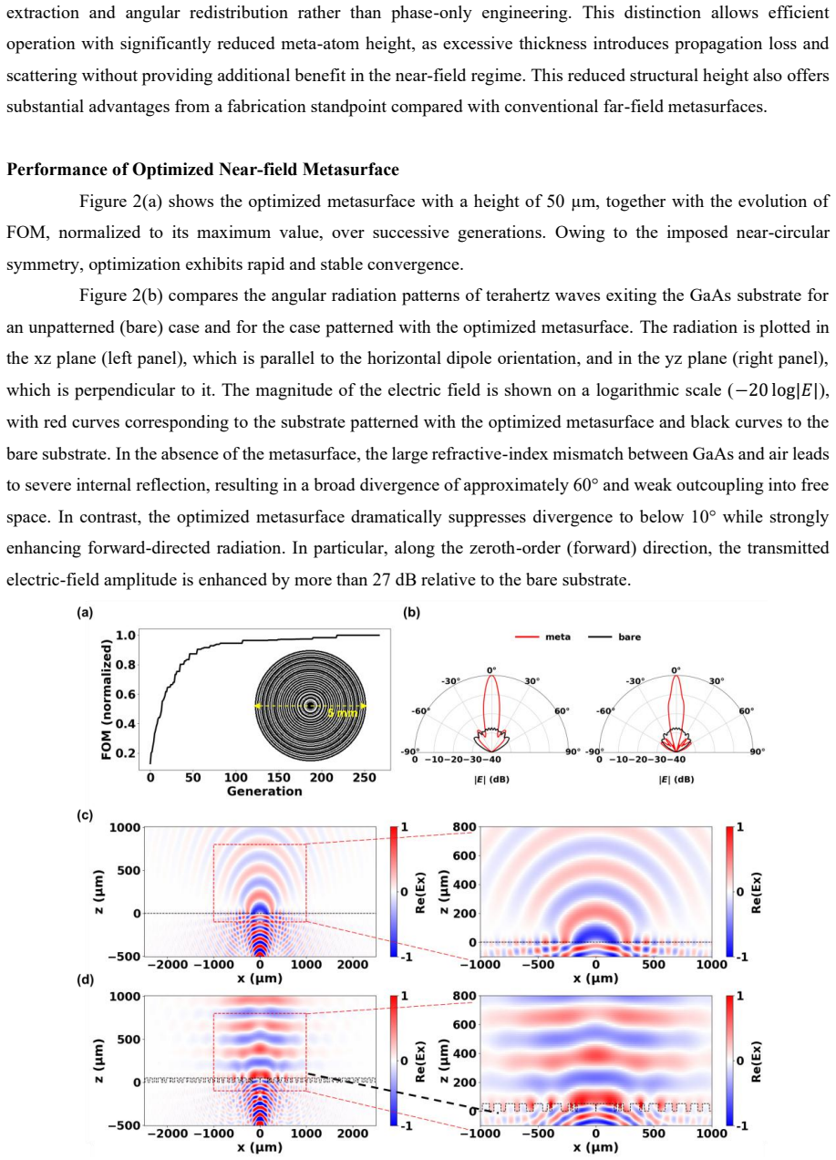
By integrating an inverse-designed dielectric metasurface directly within the near field of a terahertz photoconductive antenna, the meta-PCA collapses emission from ~60deg divergence to a sharp < 10deg forward beam, while enhancing on-axis intensity 50-fold compared to bare GaAs and exceeding the outcoupling efficiency of a bulky silicon lens by 10% despite a volume reduction of over three orders of magnitude. This shows that the metasurface co-defines the emission process itself through strong source-structure coupling.
What carries the argument
Inverse-designed dielectric metasurface integrated in the near field of the photoconductive antenna, enabling simultaneous control of emission and radiation via strong electromagnetic coupling.
If this is right
- The device achieves extreme lateral and vertical compactness while surpassing bulky conventional optics in efficiency.
- Near-field placement reduces required metasurface thickness to one-third that of reciprocal far-field designs.
- The approach enables high-efficiency, on-chip sources without post-emission decoupling assumptions.
- The same co-design principle applies across the electromagnetic spectrum for ultra-compact photonic systems.
Where Pith is reading between the lines
- The method could be tested on other source types, such as optical emitters, to check whether near-field coupling produces similar directivity gains.
- Inverse-design algorithms may need to optimize the coupled source-metasurface system explicitly rather than treating the source as fixed.
- Active tuning of the metasurface could allow dynamic control of both emission and beam direction in a single compact layer.
Load-bearing premise
The metasurface interacts strongly enough with the source in the near field to shape the emission process itself rather than merely filtering an already-emitted wave.
What would settle it
An experiment that measures unchanged antenna impedance or emission spectrum when the metasurface is added, showing the structure only acts after emission rather than participating in it.
Figures

read the original abstract
Metasurfaces have revolutionized compact wavefront control using planar, subwavelength structures. However, conventional meta-optical devices predominantly operate within a far-field paradigm, assuming electromagnetic decoupling between the source and metasurface, which limits control to post-emission wavefront shaping. Here, we define and experimentally demonstrate near-field meta-optics - a regime where strong source - structure coupling enables simultaneous control of emission and radiation. By integrating an inverse-designed dielectric metasurface directly within the near field of a terahertz photoconductive antenna (PCA), we show that the metasurface co-defines the emission process itself. Our meta-PCA, incorporating a 50-um-high metasurface - one-third the thickness required by reciprocal far-field designs - collapses emission from ~60deg divergence to a sharp < 10deg forward beam, while enhancing on-axis intensity 50-fold compared to bare GaAs. Unlike far-field metasurfaces that typically trade efficiency for thinness while remaining laterally large, our device achieves extreme compactness in both dimensions. Remarkably, it exceeds the outcoupling efficiency of a bulky, millimeter-scale silicon lens by 10%, despite a volume reduction of over three orders of magnitude. These results establish near-field meta-optics as a transformative paradigm for developing high-efficiency, ultra-compact on-chip photonic systems across the electromagnetic spectrum.
Editorial analysis
A structured set of objections, weighed in public.
Referee Report
Summary. The manuscript introduces near-field meta-optics as a regime of strong source-structure coupling, experimentally realized by integrating an inverse-designed dielectric metasurface directly within the near field of a terahertz photoconductive antenna (PCA). The resulting meta-PCA is reported to collapse emission divergence from ~60° to <10°, deliver a 50-fold on-axis intensity enhancement relative to bare GaAs, and exceed the outcoupling efficiency of a millimeter-scale silicon lens by 10% while reducing device volume by more than three orders of magnitude.
Significance. If the near-field coupling interpretation is substantiated, the work could establish a new design paradigm for ultra-compact, high-efficiency on-chip sources across the electromagnetic spectrum, moving meta-optics beyond post-emission wavefront shaping.
major comments (2)
- [Results] Results section: The load-bearing claim that the metasurface 'co-defines the emission process' itself (rather than acting as a passive post-emission collimator) is not supported by any decoupled reference simulation (metasurface treated as far-field element with fixed source) or direct measurement of altered antenna-gap fields or current distribution. The reported 50-fold boost and <10° beam are consistent with either regime.
- [Methods] Methods/Experimental section: The abstract's quantitative performance claims (50-fold intensity enhancement, 10% efficiency advantage over Si lens) are presented without any description of the measurement setup, error bars, calibration, background subtraction, or control devices, preventing assessment of the data reliability.
minor comments (2)
- [Abstract] Abstract: The statement that the 50-μm metasurface is 'one-third the thickness required by reciprocal far-field designs' lacks a specific citation or comparison to the referenced far-field thickness.
- [Figures] Figure captions: Several performance plots would benefit from explicit indication of the bare-GaAs reference curve and the Si-lens reference for direct visual comparison.
Simulated Author's Rebuttal
We thank the referee for their thoughtful and constructive review. The comments highlight important aspects of substantiating the near-field coupling regime and ensuring experimental transparency. We address each major comment below and have revised the manuscript to strengthen the presentation.
read point-by-point responses
-
Referee: [Results] Results section: The load-bearing claim that the metasurface 'co-defines the emission process' itself (rather than acting as a passive post-emission collimator) is not supported by any decoupled reference simulation (metasurface treated as far-field element with fixed source) or direct measurement of altered antenna-gap fields or current distribution. The reported 50-fold boost and <10° beam are consistent with either regime.
Authors: We agree that explicit comparison to a far-field regime is necessary to substantiate the near-field co-definition claim. In the revised manuscript we have added FDTD simulations treating the metasurface as a far-field element with an unchanged source distribution; these show that the observed <10° collimation and 50-fold on-axis boost cannot be reproduced without the strong near-field interaction. We have also included additional simulations of the modified electric-field distribution and current density within the antenna gap when the metasurface is placed in the near field. These results are now presented in a new supplementary figure and discussed in the Results section to distinguish the two regimes. revision: yes
-
Referee: [Methods] Methods/Experimental section: The abstract's quantitative performance claims (50-fold intensity enhancement, 10% efficiency advantage over Si lens) are presented without any description of the measurement setup, error bars, calibration, background subtraction, or control devices, preventing assessment of the data reliability.
Authors: We acknowledge that the original Methods section lacked sufficient detail on the experimental procedures. The revised manuscript now includes an expanded Methods section describing the THz time-domain spectroscopy setup, the precise positioning of the metasurface relative to the PCA, the calibration protocol using a reference silicon lens and bare GaAs devices, background subtraction via time-gating, error estimation from repeated measurements (standard deviation reported), and the control samples used for the efficiency comparison. These additions allow direct assessment of the reported 50-fold enhancement and 10% efficiency advantage. revision: yes
Circularity Check
No circularity: experimental results with independent validation
full rationale
The paper's core claims rest on fabrication and direct experimental measurements of a meta-PCA device, including beam divergence, intensity enhancement, and efficiency comparisons to a silicon lens. No mathematical derivation chain, fitted parameter renamed as prediction, or self-referential equation is present in the provided text or abstract. Inverse design is used as a tool to create the structure, but the reported performance metrics are measured outcomes, not outputs forced by the design equations themselves. Any self-citations (if present) do not bear the load of the central experimental demonstration, which remains falsifiable via independent replication.
Axiom & Free-Parameter Ledger
Reference graph
Works this paper leans on
-
[1]
Yu, N. et al. Light propagation with phase discontinuities: generalized laws of reflection and refraction. Science (1979). 334, 333–337 (2011)
work page 1979
-
[2]
Khorasaninejad, M. & Capasso, F. Metalenses: Versatile multifunctional photonic components. Science (1979). 358, (2017)
work page 1979
-
[3]
Chen, W. T., Zhu, A. Y., Sisler, J., Bharwani, Z. & Capasso, F. A broadband achromatic polarization - insensitive metalens consisting of anisotropic nanostructures. Nat. Commun. 10, 355 (2019)
work page 2019
-
[4]
Joo, W.-J. et al. Metasurface-driven OLED displays beyond 10,000 pixels per inch. Science (1979). 370, 459–463 (2020)
work page 1979
-
[5]
Pan, M. et al. Dielectric metalens for miniaturized imaging systems: progress and challenges. Light Sci. Appl. 11, 195 (2022)
work page 2022
-
[6]
Schulz, S. A. et al. Roadmap on photonic metasurfaces. Appl. Phys. Lett. 124, (2024)
work page 2024
-
[7]
Kuznetsov, A. I. et al. Roadmap for Optical Metasurfaces. ACS Photonics 11, 816–865 (2024)
work page 2024
-
[8]
Gopakumar, M. et al. Full-colour 3D holographic augmented-reality displays with metasurface waveguides. Nature 629, 791–797 (2024)
work page 2024
-
[9]
Yu, N. & Capasso, F. Flat optics with designer metasurfaces. Nat. Mater. 13, 139–150 (2014)
work page 2014
-
[10]
Khorasaninejad, M. et al. Metalenses at visible wavelengths: Diffraction-limited focusing and subwavelength resolution imaging. Science (1979). 352, 1190–1194 (2016)
work page 1979
-
[11]
Kildishev, A. V, Boltasseva, A. & Shalaev, V. M. Planar Photonics with Metasurfaces. Science (1979). 339, 1232009 (2013)
work page 1979
-
[12]
Arbabi, A., Horie, Y., Ball, A. J., Bagheri, M. & Faraon, A. Subwavelength -thick Lenses with High Numerical Apertures and Large Efficiency Based on High Contrast Transmitarrays. Nat. Commun. 6, 1– 10 (2015)
work page 2015
-
[13]
Kim, Y.-B., Cho, J.-W., Bae, D. & Kim, S.-K. Single-unit metalens integrated micro light-emitting diodes. Current Applied Physics 67, 85–92 (2024)
work page 2024
-
[14]
Arbabi, A., Briggs, R. M., Horie, Y., Bagheri, M. & Faraon, A. Efficient dielectric metasurface collimating lenses for mid-infrared quantum cascade lasers. Opt. Express 23, 33310–33317 (2015)
work page 2015
-
[15]
Chen, E. et al. Broadband beam collimation metasurface for full-color micro-LED displays. Opt. Express 32, 10252–10264 (2024)
work page 2024
-
[16]
Suzuki, T., Endo, K. & Kondoh, S. Terahertz metasurface ultra-thin collimator for power enhancement. Opt. Express 28, 22165–22178 (2020). 10 / 10
work page 2020
-
[18]
Roy, T. R., Sunder Meetei, T. & Yu, N. E. Design of a metalens for beam collimation and angular amplification in optical phased array devices. Opt. Express 32, 34344–34355 (2024)
work page 2024
-
[19]
Yu, Q. et al. All-Dielectric Meta-lens Designed for Photoconductive Terahertz Antennas. IEEE Photonics J. 9, 1–9 (2017)
work page 2017
-
[20]
Neu, J. & Schmuttenmaer, C. A. Tutorial: An introduction to terahertz time domain spectroscopy (THz - TDS). J. Appl. Phys. 124, (2018)
work page 2018
-
[21]
Koch, M., Mittleman, D. M., Ornik, J. & Castro-Camus, E. Terahertz time-domain spectroscopy. Nature Reviews Methods Primers 3, 48 (2023)
work page 2023
-
[22]
Burford, N. M. & El-Shenawee, M. O. Review of terahertz photoconductive antenna technology. Optical Engineering 56, 010901 (2017)
work page 2017
-
[23]
Van Rudd, J. & Mittleman, D. M. Influence of substrate-lens design in terahertz time-domain spectroscopy. Journal of the Optical Society of America B 19, 319 (2002)
work page 2002
-
[24]
Li, Z., Pestourie, R., Lin, Z., Johnson, S. G. & Capasso, F. Empowering Metasurfaces with Inverse Design: Principles and Applications. ACS Photonics 9, 2178–2192 (2022)
work page 2022
-
[25]
Elsawy, M. M. R., Lanteri, S., Duvigneau, R., Fan, J. A. & Genevet, P. Numerical Optimization Methods for Metasurfaces. Laser Photon. Rev. 14, 1900445 (2020)
work page 2020
-
[26]
Jeong, J.-Y., Latif, S. & So, S. A Tutorial on Inverse Design Methods for Metasurfaces. Current Optics and Photonics 8, 531–544 (2024)
work page 2024
-
[27]
Zhang, J., Wang, G., Wang, T. & Li, F. Genetic Algorithms to Automate the Design of Metasurfaces for Absorption Bandwidth Broadening. ACS Appl. Mater. Interfaces 13, 7792–7800 (2021)
work page 2021
-
[28]
Jafar-Zanjani, S., Inampudi, S. & Mosallaei, H. Adaptive Genetic Algorithm for Optical Metasurfaces Design. Sci. Rep. 8, 11040 (2018)
work page 2018
-
[29]
Wang, Y. et al. Genetic algorithm-enhanced design of ultra-broadband tunable terahertz metasurface absorber. Opt. Laser Technol. 170, 110262 (2024)
work page 2024
-
[30]
Tao, E. et al. Neural network and genetic algorithm-driven inverse design of a full-phase metasurface for wavefront manipulation. Journal of the Optical Society of America B 42, 2198–2206 (2025)
work page 2025
-
[31]
Katoch, S., Chauhan, S. S. & Kumar, V. A review on genetic algorithm: past, present, and future. Multimed. Tools Appl. 80, 8091–8126 (2021)
work page 2021
-
[32]
Whiting, E. B., Kang, L., Jenkins, R. P., Campbell, S. D. & Werner, D. H. Broadband plasmonic chiral meta-mirrors. Opt. Express 31, 22415–22423 (2023)
work page 2023
-
[33]
Seo, D.-J. & Kyoung, J. Shape dependence of all-dielectric terahertz metasurface. Opt. Express 30, 38564 (2022)
work page 2022
-
[34]
Yu-Jin Nam & Jisoo Kyoung. Software-based Simple Lock-in Amplifier and Built-in Sound Card for Compact and Cost-effective Terahertz Time-domain Spectroscopy System. Current Optics and Photonics 7, 683–691 (2023)
work page 2023
-
[35]
Tan, Z.-K. et al. Bright light-emitting diodes based on organometal halide perovskite. Nat. Nanotechnol. 9, 687–692 (2014)
work page 2014
-
[36]
Withers, F. et al. Light-emitting diodes by band-structure engineering in van der Waals heterostructures. Nat. Mater. 14, 301–306 (2015)
work page 2015
discussion (0)
Sign in with ORCID, Apple, or X to comment. Anyone can read and Pith papers without signing in.