Chips in the Flatland : 2D Semiconductors for Future Computing Electronic
Pith reviewed 2026-06-29 14:57 UTC · model grok-4.3
The pith
Multiscale compact modeling is the required bridge to turn 2D semiconductor transistors into functional integrated circuits.
A machine-rendered reading of the paper's core claim, the machinery that carries it, and where it could break.
Core claim
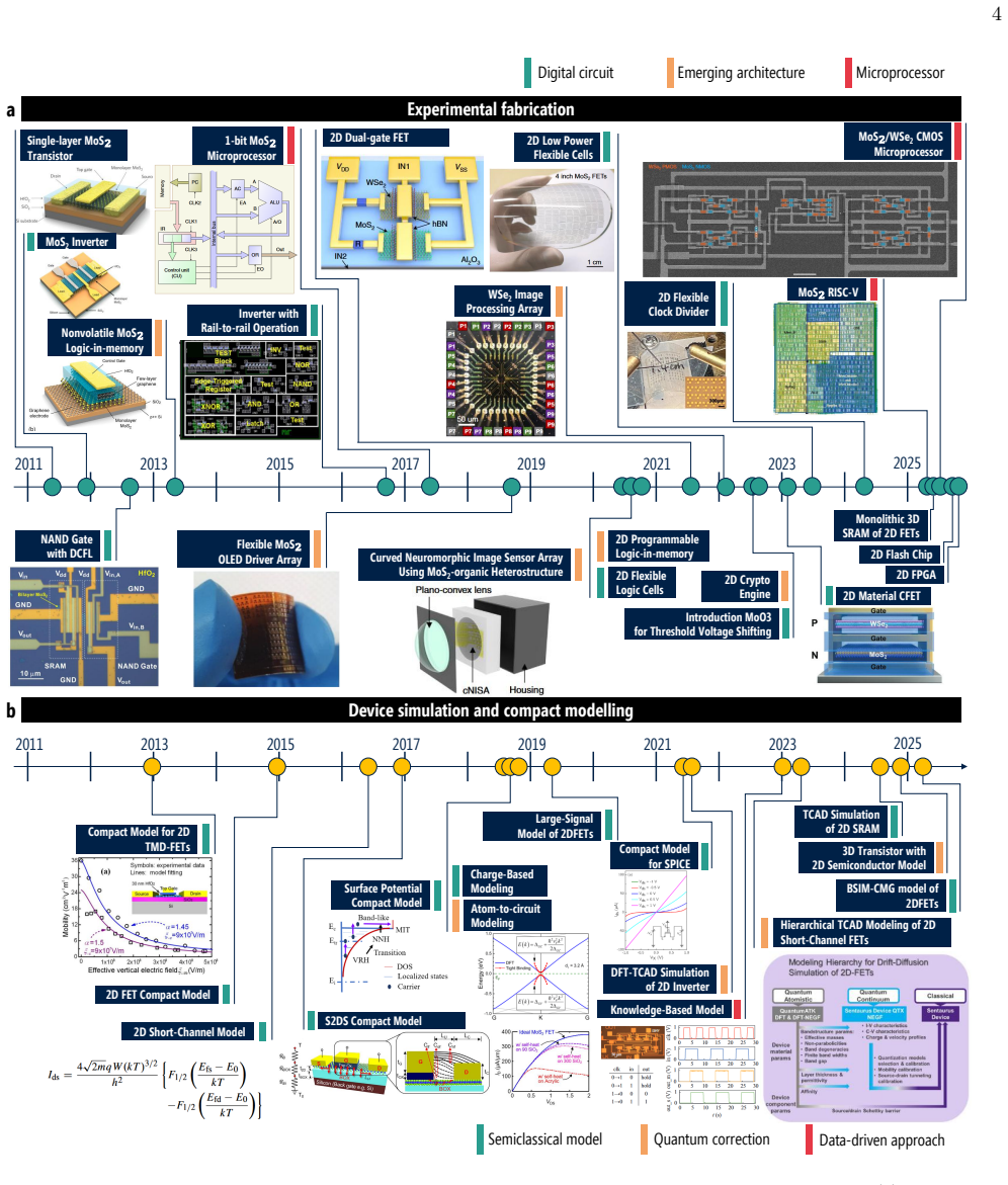
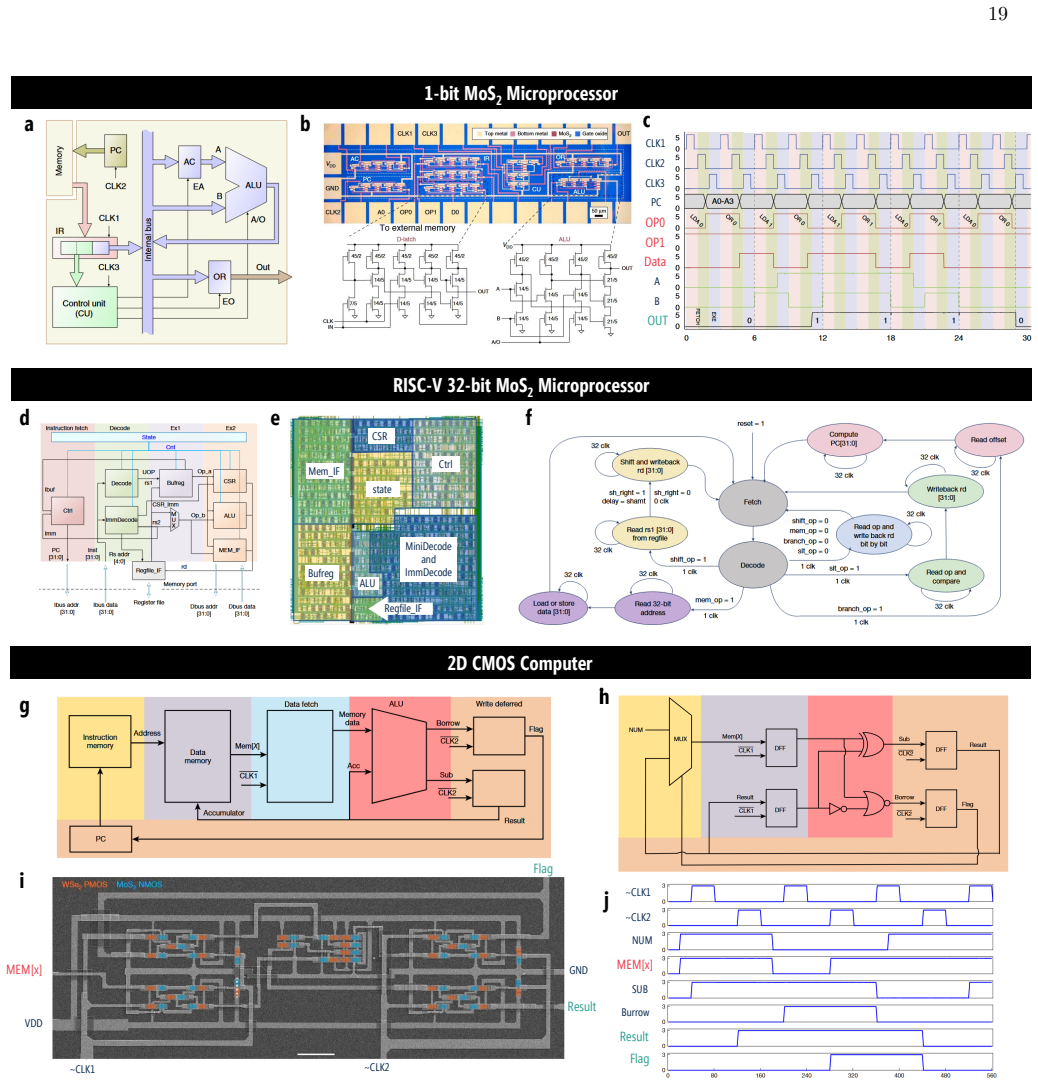
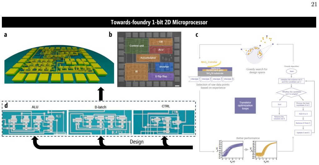
The review tracks the evolution of 2D semiconductor FETs from basic logic families and standard cells to complex chip architectures including recent RISC-V and monolithic CMOS microprocessors, while establishing multiscale compact modeling as the indispensable link between device physics and electronic design automation workflows for scalable chip development, and summarizing breakthroughs alongside fab and fabless bottlenecks.
What carries the argument
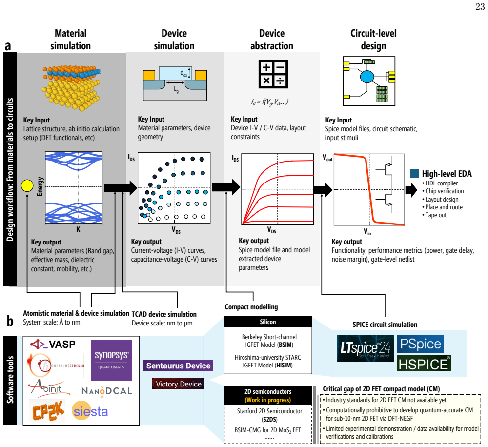
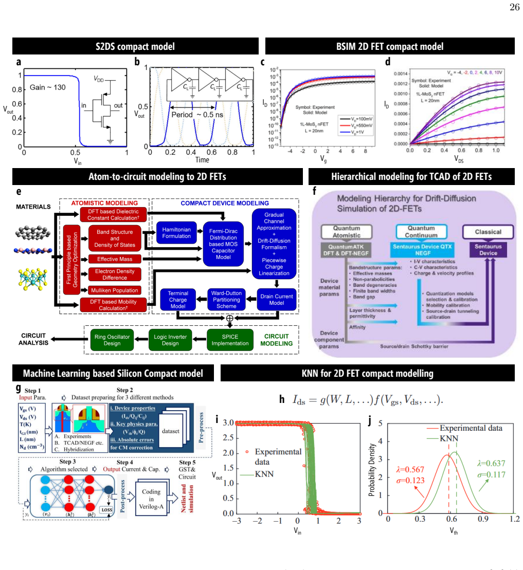
Multiscale compact modeling (semiclassical, quantum-hybrid, and data-driven approaches) that links device physics to electronic design automation workflows.
If this is right
- Milestones demonstrate that 2D materials can support complex processor architectures beyond single transistors.
- Compact modeling enables the use of standard EDA tools for 2D-based chip design.
- Mapping fab and fabless bottlenecks identifies concrete next steps for scaling.
- The overall path supports 2D semiconductors as candidates for Angstrom-era computing.
Where Pith is reading between the lines
- If compact models reach sufficient accuracy, they could shorten the timeline from material discovery to tape-out of small circuits.
- The same modeling strategy might extend to hybrid 2D-silicon stacks or other emerging channel materials.
- A practical test would be to extract parameters from a specific 2D FET and simulate a small logic block to check agreement with measured behavior.
Load-bearing premise
The cited milestones in RISC-V and monolithic CMOS processors using 2D materials are representative enough to guide general translation strategies, and the main barriers are fab and fabless issues rather than unresolved material or integration physics.
What would settle it
A working 2D-material microprocessor fabricated and verified without multiscale compact modeling, or a clear failure to reach functional integration even after deploying such models due to unaccounted physical effects.
Figures









read the original abstract
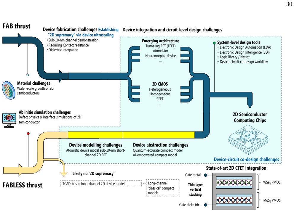
As transistor scaling approaches its fundamental physical limits in the Angstrom era, two-dimensional (2D) semiconductors have emerged as the promising channel material candidates for future computing. While the device physics of 2D semiconductors have been rigorously explored, translating these nanodevices into fully functional integrated circuits remains a largely uncharted frontier. This review bridges the gap between material- and device-centric breakthroughs and circuit-level chip design in 2D semiconductors, a valley of death that has so far prevented translation of high-performance individual transistors into functional chips. We track the evolution of 2D semi-conductor field-effect transistors from basic Boolean logic families and standard cells to complex chip architectures, including recent milestones in RISC-V and monolithic CMOS microprocessors. Critically, we highlight the indispensable role of multiscale compact modeling, spanning semiclassical, quantum-hybrid and data-driven approaches, as the necessary link between device physics and the electronic design automation workflows for scalable chip development. By summarizing recent breakthroughs and identifying the bottlenecks in both fab and fabless trajectories of 2D semiconductors, this review shall provide insights that motivates the translation of proof-of-concept 2D transistors into fully functional computing chips, paving a way towards future Angstrom era computing technology empowered by 2D semiconductors.
Editorial analysis
A structured set of objections, weighed in public.
Referee Report
Summary. This review paper tracks the development of 2D semiconductor FETs from basic Boolean logic and standard cells through to complex chip architectures, citing recent RISC-V and monolithic CMOS microprocessor milestones. It positions multiscale compact modeling (semiclassical, quantum-hybrid, and data-driven) as the indispensable bridge between device physics and EDA workflows, while identifying fab and fabless bottlenecks as the primary barriers preventing translation of high-performance transistors into functional chips.
Significance. If the cited milestones are representative and the modeling emphasis is substantiated, the review could usefully organize the literature on scaling 2D devices to circuits and motivate targeted research on compact models. However, its value as a bridge document is limited by the absence of quantitative case studies linking specific modeling advances to the cited chip-level demonstrations.
major comments (2)
- [Abstract] Abstract: The central claim that multiscale compact modeling constitutes the 'necessary link' and 'indispensable role' for scalable chip development rests on the cited RISC-V and monolithic CMOS milestones as evidence of translation progress. No section in the provided abstract or structure demonstrates that these milestones have reached a stage where modeling (rather than contact resistance, dielectric integration, or variability) is the rate-limiting step, weakening the bottleneck diagnosis.
- [Abstract] Abstract: The review asserts that 'translating these nanodevices into fully functional integrated circuits remains a largely uncharted frontier' and that fab/fabless trajectories are the primary barriers. This framing is load-bearing for the call to action, yet the abstract provides no explicit comparison showing that the cited milestones are limited by modeling gaps versus fundamental material or integration physics issues outside the review's scope.
minor comments (2)
- [Title] Title: 'Future Computing Electronic' appears incomplete or typographically inconsistent with standard phrasing ('Electronics').
- [Abstract] Abstract: 'semi-conductor' uses an inconsistent hyphenation compared to the standard 'semiconductor' used elsewhere in the abstract.
Simulated Author's Rebuttal
We thank the referee for the constructive comments on our review manuscript. We address the two major comments on the abstract point by point below and agree that targeted revisions to the abstract will better substantiate the positioning of multiscale compact modeling.
read point-by-point responses
-
Referee: [Abstract] Abstract: The central claim that multiscale compact modeling constitutes the 'necessary link' and 'indispensable role' for scalable chip development rests on the cited RISC-V and monolithic CMOS milestones as evidence of translation progress. No section in the provided abstract or structure demonstrates that these milestones have reached a stage where modeling (rather than contact resistance, dielectric integration, or variability) is the rate-limiting step, weakening the bottleneck diagnosis.
Authors: We acknowledge that the abstract, as currently worded, does not explicitly demonstrate through comparison that modeling has become the rate-limiting step versus other integration challenges. The manuscript reviews the cited milestones to illustrate progress from devices to circuits and argues, based on the surveyed literature, that compact modeling is required to bridge to EDA workflows. To address the concern, we will revise the abstract to include a concise statement noting that the review identifies modeling gaps as a key translational barrier in the context of the milestones, while recognizing that material and integration issues also remain active areas of research. revision: yes
-
Referee: [Abstract] Abstract: The review asserts that 'translating these nanodevices into fully functional integrated circuits remains a largely uncharted frontier' and that fab/fabless trajectories are the primary barriers. This framing is load-bearing for the call to action, yet the abstract provides no explicit comparison showing that the cited milestones are limited by modeling gaps versus fundamental material or integration physics issues outside the review's scope.
Authors: We agree that the abstract would benefit from an explicit qualifier on the relative role of modeling versus other physics issues. The full manuscript surveys both device-level challenges and the fab/fabless bottlenecks, using the milestones to highlight the current state of translation. We will revise the abstract to add a brief clause clarifying that, while material and integration challenges persist, the review focuses on multiscale modeling as the critical link for scalable circuit design based on the reviewed works. revision: yes
Circularity Check
Review paper with no derivations or predictions; no circularity present
full rationale
The manuscript is a literature review that summarizes device physics, milestones in RISC-V and monolithic CMOS using 2D materials, and the role of multiscale compact modeling. It contains no original equations, first-principles derivations, fitted parameters presented as predictions, or self-referential claims. The central narrative relies on external citations for milestones and bottlenecks rather than any chain that reduces by construction to its own inputs. No load-bearing step matches any of the enumerated circularity patterns.
Axiom & Free-Parameter Ledger
Reference graph
Works this paper leans on
-
[1]
Data-driven compact modelling The data-driven approach represents an emerging methodology for the compact modelling of 2D semi- conductors. Instead of explicitly formulating device behavior from material physics and transport models, data-driven compact modelling uses machine-learning (ML) models trained on numerical simulation or ex- perimental measureme...
-
[2]
(b, c) Performance projection of Si and 2D SRAM [81] (b) Schematic of 6T SRAM (c) Si and 2D SRAM performance from various technology node (d, e) Performance projection of Si and 2D GAAFET SRAM [179] (d) Illustration of GAAFET SRAM (e) Si, 2D SRAM, 2D SRAM with optimization, and 2D nanosheet SRAM performance By combining device-level geometric inputs with ...
-
[3]
2D supremacy
[Fig. 16(b)] indicate that 2D-semiconductor-based SRAMs can achieve improved timing characteristics com- pared to silicon counterparts. Read-access time improves with technology scaling, reaching up to 16% improvement at the 1 nm node [Fig. 16(c)]. Write time and dynamic power exhibit their greatest improvements, i.e. 72% and 60%, respectively, around the...
2012
-
[4]
More Moore
(Ref.c) CMOS OISC 2D computer [67] (Ref.d) Towards-foundry 2D microprocessor [158] critically, at the system level, fault-tolerant chip design should also form a crucial principle for ensuring the relia- bility of complex circuits and failure-sensitive chips [55]. For silicon, many design techniques have been adopted to overcome yield challenges. A common...
2017
-
[5]
Auth and A
C. Auth and A. Shankar, Evolution of Transistors: Humble Beginnings to the Ubiquitous Present, IEEE Solid-State Circuits Magazine 15, 20 (2023)
2023
-
[6]
Furber, Microprocessors: The engines of the digital age, Proceedings of the Royal Society A: Mathemati- cal, Physical and Engineering Sciences 473, 20160893 (2017)
S. Furber, Microprocessors: The engines of the digital age, Proceedings of the Royal Society A: Mathemati- cal, Physical and Engineering Sciences 473, 20160893 (2017)
2017
-
[7]
M. S. Lundstrom and M. A. Alam, Moore’s law: The journey ahead, Science 378, 722 (2022)
2022
-
[8]
Inc., Apple reveals m3 ultra, taking apple silicon to a new extreme, Apple Newsroom (press release) (2025), accessed: 2025-10-07
A. Inc., Apple reveals m3 ultra, taking apple silicon to a new extreme, Apple Newsroom (press release) (2025), accessed: 2025-10-07
2025
-
[9]
R. F. Service, Chipmakers look past Moore’s law, and silicon, Science 361, 321 (2018)
2018
-
[10]
J. Shalf, The future of computing beyond Moore’s Law, Philosophical Transactions of the Royal Society A 10.1098/rsta.2019.0061 (2020)
-
[11]
Li, S.-K
M.-Y. Li, S.-K. Su, H.-S. P. Wong, and L.-J. Li, How 2D semiconductors could extend Moore’s law, Nature (London) 567, 169 (2019)
2019
-
[12]
Waltl, T
M. Waltl, T. Knobloch, K. Tselios, L. Filipovic, B. Stampfer, Y. Hernandez, D. Waldh¨ or, Y. Illarionov, B. Kaczer, and T. Grasser, Perspective of 2D Integrated Electronic Circuits: Scientific Pipe Dream or Disruptive Technology?, Advanced Materials 34, 2201082 (2022)
2022
-
[13]
S. Wang, X. Liu, M. Xu, L. Liu, D. Yang, and P. Zhou, Two-dimensional devices and integration towards the silicon lines, Nature Materials 21, 1225 (2022)
2022
-
[14]
X. Chen, S. M. Shinde, K. P. Dhakal, S. W. Lee, H. Kim, Z. Lee, and J.-H. Ahn, Degradation behaviors and mech- anisms of MoS2 crystals relevant to bioabsorbable elec- tronics, NPG Asia Materials 10, 810 (2018)
2018
-
[15]
Y. Xia, X. Chen, J. Wei, S. Wang, S. Chen, S. Wu, M. Ji, Z. Sun, Z. Xu, W. Bao, and P. Zhou, 12-inch growth of uniform MoS2 monolayer for integrated cir- cuit manufacture, Nature Materials 22, 1324 (2023)
2023
-
[16]
Knobloch, B
T. Knobloch, B. Uzlu, Y. Y. Illarionov, Z. Wang, M. Otto, L. Filipovic, M. Waltl, D. Neumaier, M. C. Lemme, and T. Grasser, Improving stability in two- dimensional transistors with amorphous gate oxides by Fermi-level tuning, Nature Electronics 5, 356 (2022)
2022
-
[17]
M. W. Iqbal, M. Z. Iqbal, M. F. Khan, M. A. She- hzad, Y. Seo, J. H. Park, C. Hwang, and J. Eom, High-mobility and air-stable single-layer WS2 field- effect transistors sandwiched between chemical vapor deposition-grown hexagonal BN films, Scientific Reports 5, 10699 (2015)
2015
-
[18]
Lan, C.-P
H.-Y. Lan, C.-P. Lin, L. Liu, J. Cai, Z. Sun, P. Wu, Y. Tan, S.-H. Yang, T.-H. Hou, J. Appenzeller, and Z. Chen, Uncovering the doping mechanism of nitric ox- ide in high-performance P-type WSe2 transistors, Na- ture Communications 16, 4160 (2025)
2025
-
[19]
G. Wang, W. J. Slough, R. Pandey, and S. P. Karna, Degradation of phosphorene in air: Understanding at atomic level, 2D Materials 3, 025011 (2016)
2016
-
[20]
D. He, Y. Wang, Y. Huang, Y. Shi, X. Wang, and X. Duan, High-Performance Black Phosphorus Field- Effect Transistors with Long-Term Air Stability, Nano Letters 19, 331 (2019)
2019
-
[21]
Huang, B
H. Huang, B. Jiang, X. Zou, X. Zhao, and L. Liao, Black phosphorus electronics, Science Bulletin Two- Dimensional Materials: New Opportunities for Elec- tronics, Photonics and Optoelectronics,64, 1067 (2019)
2019
-
[22]
Jiang, J
J. Jiang, J. Li, Y. Li, J. Duan, L. Li, Y. Tian, Z. Zong, H. Zheng, X. Feng, Q. Li, H. Liu, Y. Zhang, T.-L. Ren, and L. Han, Stable InSe transistors with high-field ef- fect mobility for reliable nerve signal sensing, npj 2D Materials and Applications 3, 29 (2019). 36
2019
-
[23]
M. J. Hamer, J. Zultak, A. V. Tyurnina, V. Z´ olyomi, D. Terry, A. Barinov, A. Garner, J. Donoghue, A. P. Rooney, V. Kandyba, A. Giampietri, A. Graham, N. Teutsch, X. Xia, M. Koperski, S. J. Haigh, V. I. Fal’ko, R. V. Gorbachev, and N. R. Wilson, Indirect to Direct Gap Crossover in Two-Dimensional InSe Re- vealed by Angle-Resolved Photoemission Spectrosco...
2019
-
[24]
Zavabeti, P
A. Zavabeti, P. Aukarasereenont, H. Tuohey, N. Syed, A. Jannat, A. Elbourne, K. A. Messalea, B. Y. Zhang, B. J. Murdoch, J. G. Partridge, M. Wur- dack, D. L. Creedon, J. van Embden, K. Kalantar- Zadeh, S. P. Russo, C. F. McConville, and T. Daeneke, High-mobility p-type semiconducting two-dimensional β-TeO2, Nature Electronics 4, 277 (2021)
2021
-
[25]
Wang, J.-W
Y.-J. Wang, J.-W. Zhang, J. Chen, H. Wang, S. Wu, C.-Y. Lo, J.-T. Hong, C.-Y. Syu, L.-S. Hao, I.-S. Chen, Y.-C. Chang, Z. Yang, R. Huang, C.-L. Lin, P.-W. Chiu, Y.-L. Chueh, Y.-C. Chen, C.-H. Yeh, and Y.- H. Chu, Polarity modulation in compositionally tunable Bi2O2Se thin films, Nature Communications 16, 2873 (2025)
2025
-
[26]
M. Yu, C. Tan, Y. Yin, J. Tang, X. Gao, H. Liu, F. Ding, and H. Peng, Integrated 2D multi-fin field-effect tran- sistors, Nature Communications 15, 3622 (2024)
2024
-
[27]
Meena, N
S. Meena, N. Sharma, and J. Jogi, Sub-5 nm 2D Semiconductor-Based Monolayer Field-Effect Transis- tor: Status and Prospects, physica status solidi (a) 220, 2200526 (2023)
2023
-
[28]
Sebastian, R
A. Sebastian, R. Pendurthi, T. H. Choudhury, J. M. Redwing, and S. Das, Benchmarking monolayer MoS2 and WS2 field-effect transistors, Nature Communica- tions 12, 693 (2021)
2021
-
[29]
S. B. Desai, S. R. Madhvapathy, A. B. Sachid, J. P. Llinas, Q. Wang, G. H. Ahn, G. Pitner, M. J. Kim, J. Bokor, C. Hu, H.-S. P. Wong, and A. Javey, MoS2 transistors with 1-nanometer gate lengths, Science 354, 99 (2016)
2016
-
[30]
Cheng, J
Q. Cheng, J. Pang, D. Sun, J. Wang, S. Zhang, F. Liu, Y. Chen, R. Yang, N. Liang, X. Lu, Y. Ji, J. Wang, C. Zhang, Y. Sang, H. Liu, and W. Zhou, WSe2 2D p-type semiconductor-based electronic devices for infor- mation technology: Design, preparation, and applica- tions, InfoMat 2, 656 (2020)
2020
-
[31]
X. Wang, C. Liu, Y. Wei, S. Feng, D. Sun, and H. Cheng, Three-dimensional transistors and integra- tion based on low-dimensional materials for the post- Moore’s law era, Materials Today 63, 170 (2023)
2023
-
[32]
Dutta, N
T. Dutta, N. Yadav, Y. Wu, G. J. Cheng, X. Liang, S. Ramakrishna, A. Sbai, R. Gupta, A. Mondal, Z. Hongyu, and A. Yadav, Electronic properties of 2D materials and their junctions, Nano Materials Science 6, 1 (2024)
2024
-
[33]
S. Wang, X. Liu, and P. Zhou, The Road for 2D Semi- conductors in the Silicon Age, Advanced Materials 34, 2106886 (2022)
2022
-
[34]
Y. Shen, Z. Dong, Y. Sun, H. Guo, F. Wu, X. Li, J. Tang, J. Liu, X. Wu, H. Tian, and T.-L. Ren, The Trend of 2D Transistors toward Integrated Circuits: Scaling Down and New Mechanisms, Advanced Mate- rials 34, 2201916 (2022)
2022
-
[35]
Reale, P
F. Reale, P. Palczynski, I. Amit, G. F. Jones, J. D. Mehew, A. Bacon, N. Ni, P. C. Sherrell, S. Agnoli, M. F. Craciun, S. Russo, and C. Mattevi, High-Mobility and High-Optical Quality Atomically Thin WS 2, Scientific Reports 7, 14911 (2017)
2017
-
[36]
M. Dai, C. Gao, Q. Nie, Q.-J. Wang, Y.-F. Lin, J. Chu, and W. Li, Properties, Synthesis, and Device Applica- tions of 2D Layered InSe, Advanced Materials Technolo- gies 7, 2200321 (2022)
2022
-
[37]
L. Li, Y. Yu, G. J. Ye, Q. Ge, X. Ou, H. Wu, D. Feng, X. H. Chen, and Y. Zhang, Black phosphorus field-effect transistors, Nature Nanotechnology 9, 372 (2014)
2014
-
[38]
Latychevskaia, D
T. Latychevskaia, D. A. Bandurin, and K. S. Novoselov, A new family of septuple-layer 2D materials of MoSi2N4-like crystals, Nature Reviews Physics 6, 426 (2024)
2024
-
[39]
C. C. Tho, C. Yu, Q. Tang, Q. Wang, T. Su, Z. Feng, Q. Wu, C. V. Nguyen, W.-L. Ong, S.-J. Liang, S.- D. Guo, L. Cao, S. Zhang, S. A. Yang, L. K. Ang, G. Wang, and Y. S. Ang, Cataloguing MoSi2N4 and WSi2N4 van der Waals Heterostructures: An Excep- tional Material Platform for Excitonic Solar Cell Ap- plications, Advanced Materials Interfaces 10, 2201856 (2023)
2023
-
[40]
T. Zhou, C. Xu, and W. Ren, The van der Waals MoSi2N4 materials family, Nature Reviews Materials , 1 (2025)
2025
-
[41]
M. Ao, X. Zhou, X. Kong, S. Gou, S. Chen, X. Dong, Y. Zhu, Q. Sun, Z. Zhang, J. Zhang, Q. Zhang, Y. Hu, C. Sheng, K. Wang, S. Wang, J. Wan, J. Han, W. Bao, and P. Zhou, A RISC-V 32-bit microprocessor based on two-dimensional semiconductors, Nature , 1 (2025)
2025
-
[42]
Dong, L.-S
C. Dong, L.-S. Lu, Y.-C. Lin, and J. A. Robinson, Air-Stable, Large-Area 2D Metals and Semiconductors, ACS Nanoscience Au 4, 115 (2024)
2024
-
[43]
L. Yin, J. Wang, Y. Sun, X. Liu, X. Zou, R. Cheng, H. Wang, Y. Zhu, X. Gong, Z. Liu, Y. Zhou, X. Wang, Q. Zhang, L. Yang, Z. Zhang, H. Ye, Y. Zhu, L. Tang, K. Zhang, L. Liao, R. Wang, and J. He, Recent progress in growth and applications of 2D materials, Review of Materials Research 1, 100059 (2025)
2025
-
[44]
Lanza, Q
M. Lanza, Q. Smets, C. Huyghebaert, and L.-J. Li, Yield, variability, reliability, and stability of two- dimensional materials based solid-state electronic de- vices, Nature Communications 11, 5689 (2020)
2020
-
[45]
Zhang, J
F. Zhang, J. Song, Y. Yan, F. Wang, P. Zhang, Y. Cai, Z. Li, Y. Zhu, Y. Wang, S. Li, X. Zhan, K. Xu, and Z. Wang, Dielectric Integrations and Advanced Inter- face Engineering for 2D Field-Effect Transistors, Small Methods , 2402187 (2025)
2025
-
[46]
Y. C. Lin, C.-M. Lin, H.-Y. Chen, S. Vaziri, X. Bao, W.- Y. Woon, H. Wang, and S. S. Liao, Dielectric Material Technologies for 2-D Semiconductor Transistor Scaling, IEEE Transactions on Electron Devices70, 1454 (2023)
2023
-
[47]
C. S. Lau, S. Das, I. A. Verzhbitskiy, D. Huang, Y. Zhang, T. Talha-Dean, W. Fu, D. Venkatakrish- narao, and K. E. Johnson Goh, Dielectrics for Two- Dimensional Transition-Metal Dichalcogenide Applica- tions, ACS Nano 17, 9870 (2023)
2023
-
[48]
M. S. Choi, N. Ali, T. D. Ngo, H. Choi, B. Oh, H. Yang, and W. J. Yoo, Recent Progress in 1D Contacts for 2D-Material-Based Devices, Advanced Materials34, 2202408 (2022)
2022
-
[49]
L. Ma, Y. Wang, and Y. Liu, Van der Waals Contact for Two-Dimensional Transition Metal Dichalcogenides, Chemical Reviews 124, 2583 (2024). 37
2024
-
[50]
L. Liu, Y. Wang, R. Dong, D. Fan, S. Meng, L. Wu, S. Wu, W. Xu, M. Feng, N. Zou, et al. , Kinetic accel- eration of mos2 growth by oxy-metal-organic chemical vapor deposition, Science 391, 494 (2026)
2026
-
[51]
Chhowalla, D
M. Chhowalla, D. Jena, and H. Zhang, Two-dimensional semiconductors for transistors, Nature Reviews Materi- als 1, 16052 (2016)
2016
-
[52]
S. Das, A. Sebastian, E. Pop, C. J. McClellan, A. D. Franklin, T. Grasser, T. Knobloch, Y. Illarionov, A. V. Penumatcha, J. Appenzeller, Z. Chen, W. Zhu, I. Assel- berghs, L.-J. Li, U. E. Avci, N. Bhat, T. D. Anthopou- los, and R. Singh, Transistors based on two-dimensional materials for future integrated circuits, Nature Electron- ics 4, 786 (2021)
2021
-
[53]
C. Liu, H. Chen, S. Wang, Q. Liu, Y.-G. Jiang, D. W. Zhang, M. Liu, and P. Zhou, Two-dimensional materi- als for next-generation computing technologies, Nature Nanotechnology 15, 545 (2020)
2020
-
[54]
Radisavljevic, A
B. Radisavljevic, A. Radenovic, J. Brivio, V. Gia- cometti, and A. Kis, Single-layer MoS2 transistors, Na- ture Nanotechnology 6, 147 (2011)
2011
-
[55]
Radisavljevic, M
B. Radisavljevic, M. B. Whitwick, and A. Kis, Inte- grated Circuits and Logic Operations Based on Single- Layer MoS2, ACS Nano 5, 9934 (2011)
2011
-
[56]
H. Wang, L. Yu, Y.-H. Lee, Y. Shi, A. Hsu, M. L. Chin, L.-J. Li, M. Dubey, J. Kong, and T. Palacios, Integrated Circuits Based on Bilayer MoS2 Transistors, Nano Let- ters 12, 4674 (2012)
2012
-
[57]
Bertolazzi, D
S. Bertolazzi, D. Krasnozhon, and A. Kis, Nonvolatile Memory Cells Based on MoS2/Graphene Heterostruc- tures, ACS Nano 7, 3246 (2013)
2013
-
[58]
L. Yu, D. El-Damak, U. Radhakrishna, X. Ling, A. Zubair, Y. Lin, Y. Zhang, M.-H. Chuang, Y.-H. Lee, D. Antoniadis, J. Kong, A. Chandrakasan, and T. Pala- cios, Design, Modeling, and Fabrication of Chemical Vapor Deposition Grown MoS2 Circuits with E-Mode FETs for Large-Area Electronics, Nano Letters16, 6349 (2016)
2016
-
[59]
Wachter, D
S. Wachter, D. K. Polyushkin, O. Bethge, and T. Mueller, A microprocessor based on a two- dimensional semiconductor, Nature Communications 8, 14948 (2017)
2017
-
[60]
Y. Woo, W. Hong, S. Y. Yang, H. J. Kim, J.-H. Cha, J. E. Lee, K. J. Lee, T. Kang, and S.-Y. Choi, Large- Area CVD-Grown MoS2 Driver Circuit Array for Flex- ible Organic Light-Emitting Diode Display, Advanced Electronic Materials 4, 1800251 (2018)
2018
-
[61]
C. Choi, J. Leem, M. Kim, A. Taqieddin, C. Cho, K. W. Cho, G. J. Lee, H. Seung, H. J. Bae, Y. M. Song, T. Hyeon, N. R. Aluru, S. Nam, and D.-H. Kim, Curved neuromorphic image sensor array using a MoS2-organic heterostructure inspired by the human visual recogni- tion system, Nature Communications 11, 5934 (2020)
2020
-
[62]
N. Li, Q. Wang, C. Shen, Z. Wei, H. Yu, J. Zhao, X. Lu, G. Wang, C. He, L. Xie, J. Zhu, L. Du, R. Yang, D. Shi, and G. Zhang, Large-scale flexible and transparent elec- tronics based on monolayer molybdenum disulfide field- effect transistors, Nature Electronics 3, 711 (2020)
2020
-
[63]
Migliato Marega, Y
G. Migliato Marega, Y. Zhao, A. Avsar, Z. Wang, M. Tripathi, A. Radenovic, and A. Kis, Logic-in- memory based on an atomically thin semiconductor, Nature 587, 72 (2020)
2020
-
[64]
H. Chen, X. Xue, C. Liu, J. Fang, Z. Wang, J. Wang, D. W. Zhang, W. Hu, and P. Zhou, Logic gates based on neuristors made from two-dimensional materials, Na- ture Electronics 4, 399 (2021)
2021
-
[65]
S. Zeng, C. Liu, X. Huang, Z. Tang, L. Liu, and P. Zhou, An application-specific image processing array based on WSe2 transistors with electrically switchable logic func- tions, Nature Communications 13, 56 (2022)
2022
-
[66]
Dodda, N
A. Dodda, N. Trainor, Joan. M. Redwing, and S. Das, All-in-one, bio-inspired, and low-power crypto engines for near-sensor security based on two-dimensional mem- transistors, Nature Communications 13, 3587 (2022)
2022
-
[67]
J. Tian, Y. Peng, Q. Wang, Y. Chu, Z. Huang, N. Li, X. Li, J. Tang, B. Huang, R. Yang, L. Du, W. Yang, D. Shi, and G. Zhang, Rail-to-Rail MoS2 Inverters, ACS Applied Electronic Materials 4, 2636 (2022)
2022
-
[68]
M. Liu, J. Niu, G. Yang, K. Chen, W. Lu, F. Liao, C. Lu, N. Lu, and L. Li, Large-Scale Ultrathin Channel Nanosheet-Stacked CFET Based on CVD 1L MoS2/WSe2, Advanced Electronic Materials9, 2200722 (2023)
2023
-
[69]
Y. Peng, C. Cui, L. Li, Y. Wang, Q. Wang, J. Tian, Z. Huang, B. Huang, Y. Zhang, X. Li, J. Tang, Y. Chu, W. Yang, D. Shi, L. Du, N. Li, and G. Zhang, Medium- scale flexible integrated circuits based on 2D semicon- ductors, Nature Communications 15, 10833 (2024)
2024
-
[70]
M. U. K. Sadaf, Z. Chen, S. Subbulakshmi Radhakrish- nan, Y. Sun, L. Ding, A. R. Graves, Y. Yang, J. M. Redwing, and S. Das, Enabling static random-access memory cell scaling with monolithic 3D integration of 2D field-effect transistors, Nature Communications 16, 4879 (2025)
2025
-
[71]
Ghosh, Y
S. Ghosh, Y. Zheng, M. Rafiq, H. Ravichandran, Y. Sun, C. Chen, M. Goswami, N. U. Sakib, M. U. K. Sadaf, A. Pannone, S. Ray, J. M. Redwing, Y. Yang, S. Sa- hay, and S. Das, A complementary two-dimensional material-based one instruction set computer, Nature 642, 327 (2025)
2025
-
[72]
C. Liu, Y. Jiang, B. Shen, S. Yuan, Z. Cao, Z. Bi, C. Wang, Y. Xiang, T. Wang, H. Wu, Z. Liu, Y. Wang, S. Wang, and P. Zhou, A full-featured 2D flash chip enabled by system integration, Nature , 1 (2025)
2025
-
[73]
Jim´ enez, Drift-diffusion model for single layer tran- sition metal dichalcogenide field-effect transistors, Ap- plied Physics Letters 101, 243501 (2012)
D. Jim´ enez, Drift-diffusion model for single layer tran- sition metal dichalcogenide field-effect transistors, Ap- plied Physics Letters 101, 243501 (2012)
2012
-
[74]
W. Cao, J. Kang, W. Liu, and K. Banerjee, A Compact Current–Voltage Model for 2D Semiconductor Based Field-Effect Transistors Considering Interface Traps, Mobility Degradation, and Inefficient Doping Effect, IEEE Transactions on Electron Devices61, 4282 (2014)
2014
-
[75]
Y. Taur, J. Wu, and J. Min, A Short-Channel I – V Model for 2-D MOSFETs, IEEE Transactions on Elec- tron Devices 63, 2550 (2016)
2016
-
[76]
S. V. Suryavanshi and E. Pop, S2DS: Physics-based compact model for circuit simulation of two-dimensional semiconductor devices including non-idealities, Journal of Applied Physics 120, 224503 (2016)
2016
-
[77]
L. Wang, Y. Li, X. Feng, K.-W. Ang, X. Gong, A. V.-Y. Thean, and G. Liang, A surface potential based com- pact model for two-dimensional field effect transistors with disorders induced transition behaviors, Journal of Applied Physics 124, 034302 (2018)
2018
-
[78]
Yadav, P
C. Yadav, P. Rastogi, T. Zimmer, and Y. S. Chauhan, Charge-Based Modeling of Transition Metal Dichalco- genide Transistors Including Ambipolar, Trapping, and Negative Capacitance Effects, IEEE Transactions on 38 Electron Devices 65, 4202 (2018)
2018
-
[79]
Das and S
B. Das and S. Mahapatra, An atom-to-circuit model- ing approach to all-2D metal–insulator–semiconductor field-effect transistors, npj 2D Materials and Applica- tions 2, 1 (2018)
2018
-
[80]
Pasadas, E
F. Pasadas, E. G. Marin, A. Toral-Lopez, F. G. Ruiz, A. Godoy, S. Park, D. Akinwande, and D. Jim´ enez, Large-signal model of 2DFETs: Compact modeling of terminal charges and intrinsic capacitances, npj 2D Ma- terials and Applications 3, 47 (2019)
2019
discussion (0)
Sign in with ORCID, Apple, or X to comment. Anyone can read and Pith papers without signing in.