Near-UV Single-Pixel Imaging with All-Inorganic Lead-Free Perovskite
Pith reviewed 2026-06-28 13:20 UTC · model grok-4.3
The pith
Lead-free K2CuBr3 photoconductors reconstruct near-UV images in single-pixel imaging with SNR rising to 31.7 dB.
A machine-rendered reading of the paper's core claim, the machinery that carries it, and where it could break.
Core claim
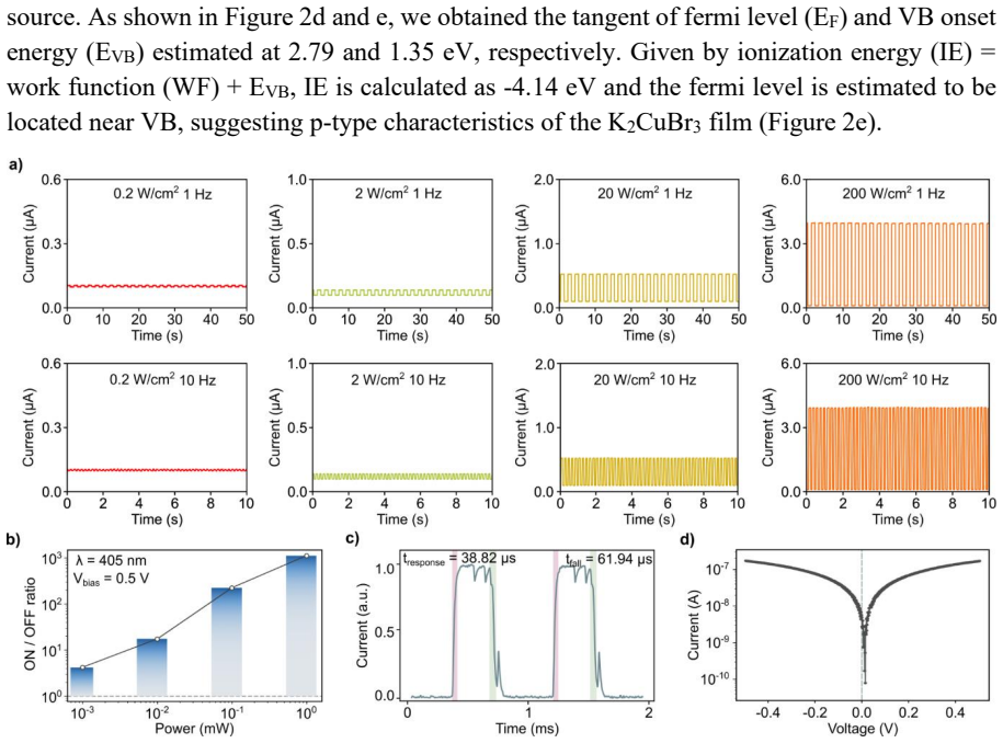
Solution-processed K2CuBr3 thin films, obtained via systematic antisolvent engineering to yield compact and uniform layers, are integrated into planar photoconductors that exhibit stable photoswitching, low dark current, and fast response under 405 nm illumination. These photoconductors, when used in a single-pixel imaging configuration, successfully reconstruct near-UV images with signal-to-noise ratio improving from 16.4 to 31.7 dB as illumination irradiance increases.
What carries the argument
The K2CuBr3 photoconductor, formed from antisolvent-engineered thin films, converts sequential near-UV illumination into optoelectrical signals for computational image reconstruction without pixelated arrays.
If this is right
- The photodetectors exhibit stable photoswitching under 405 nm illumination with low dark current on the order of 10^{-10} A.
- Response and recovery times reach 38.82 μs and 61.94 μs respectively.
- Image reconstruction succeeds in the SPI configuration with SNR scaling upward as irradiance increases.
- Solution-processed lead-free copper halides can serve as photoactive materials for compact UV computational imaging.
Where Pith is reading between the lines
- The approach could extend to other wavelengths if similar films are tuned for different absorption edges.
- Integration into portable devices might follow if the low dark current and fast switching hold in varied environments.
- Cost reductions in UV imaging systems become feasible if the one-step fabrication scales without additional toxic components.
Load-bearing premise
The antisolvent-engineered K2CuBr3 films maintain compact uniformity and stable photoswitching under 405 nm illumination sufficient for reliable image reconstruction.
What would settle it
If tests at increasing irradiance levels show no improvement in signal-to-noise ratio beyond 16.4 dB or fail to produce recognizable reconstructed near-UV images matching the input patterns, the central claim would not hold.
Figures
read the original abstract
Single-pixel imaging (SPI) is a powerful computational imaging technology that reconstructs spatial information from sequentially encoded optoelectrical signals without pixelated detector arrays. Solution-processible metal halide perovskites are promising photoactive candidates for SPI, but the toxicity of lead-based compositions remains a critical barrier to practical development. Here, we demonstrate one-step fabrication of low-dimensional, lead-free K$_2$CuBr$_3$ thin film as near-UV photoactive channels for single-pixel imaging. By systematic antisolvent engineering, compact and uniform K2CuBr3 films are obtained and integrated into planar photoconductors devices. The resulting photodetectors exhibit stale photoswitching under 405 nm illumination, low dark current on the order of $10^{-10}$ A, with fast response and recovery time 38.82 and 61.94 $\mu$s, respectively. Integrated into an SPI configuration, the K2CuBr3 photoconductor successfully reconstructs near-UV images, with the signal-to-noise ratio improving from 16.4 to 31.7 dB as the illumination irradiance increases. This work highlights solution-processed lead-free copper halides as promising photoactive materials for compact, non-toxic and cost-effective UV computational imaging systems.
Editorial analysis
A structured set of objections, weighed in public.
Referee Report
Summary. The manuscript reports one-step fabrication of low-dimensional, lead-free K₂CuBr₃ thin films via antisolvent engineering, integrated into planar photoconductors that exhibit low dark current (~10^{-10} A), fast response/recovery times (38.82/61.94 μs), and stable photoswitching under 405 nm illumination. These devices are then used in a single-pixel imaging (SPI) configuration to reconstruct near-UV images, with reported SNR improving from 16.4 to 31.7 dB as illumination irradiance increases.
Significance. If the experimental demonstration holds, the work is significant for establishing an all-inorganic, lead-free copper halide as a solution-processible photoactive material for compact, non-toxic near-UV SPI systems, addressing toxicity concerns with lead-based perovskites while achieving competitive device metrics and functional imaging performance.
major comments (1)
- [Abstract] Abstract: The central claim of successful near-UV image reconstruction with SNR rising from 16.4 to 31.7 dB is presented without raw data, error bars, device schematics, illumination conditions, or description of the reconstruction algorithm and SPI setup. These omissions make independent verification of the reported performance impossible from the supplied text and undermine the load-bearing experimental result.
minor comments (2)
- [Abstract] Abstract: 'stale photoswitching' is presumably a typo for 'stable photoswitching'.
- [Abstract] Abstract: Inconsistent subscript formatting for K₂CuBr₃ (sometimes written as K2CuBr3).
Simulated Author's Rebuttal
We thank the referee for their careful review and constructive feedback. We address the single major comment point-by-point below.
read point-by-point responses
-
Referee: [Abstract] Abstract: The central claim of successful near-UV image reconstruction with SNR rising from 16.4 to 31.7 dB is presented without raw data, error bars, device schematics, illumination conditions, or description of the reconstruction algorithm and SPI setup. These omissions make independent verification of the reported performance impossible from the supplied text and undermine the load-bearing experimental result.
Authors: Abstracts are concise summaries and are not required to contain raw data, error bars, schematics, or full algorithmic descriptions; these are standardly placed in the main text, figures, and methods to respect length constraints. The complete manuscript provides: device schematics in Figure 1; SPI setup, illumination conditions (405 nm), and irradiance values in the Experimental Section and Figure 4; the reconstruction algorithm (including any compressive sensing or Hadamard basis details) in the Methods; and SNR data with error bars and supporting measurements in Figure 5 and associated results text. Independent verification is therefore possible from the full manuscript, not the abstract alone. We do not believe revision of the abstract is necessary. revision: no
Circularity Check
No significant circularity; purely experimental report
full rationale
The manuscript contains no equations, derivations, fitted parameters, predictions, or mathematical claims. All results follow from direct fabrication (antisolvent engineering), device characterization (dark current, response times), and experimental SPI reconstruction with reported SNR values. No self-citations, ansatzes, or uniqueness theorems are invoked as load-bearing steps. The derivation chain is therefore empty and self-contained against external benchmarks.
Axiom & Free-Parameter Ledger
axioms (1)
- domain assumption Photoconductivity and carrier dynamics in inorganic semiconductors govern the observed dark current, response times, and photoswitching in K2CuBr3 films.
Reference graph
Works this paper leans on
-
[1]
Near-UV Single -Pixel Imaging with All -Inorganic Lead -Free Perovskite Jiyun Kim1, 2*, Xinyang Yu1, 2, Zijian Feng3, Chun-Ho Lin3, Dewei Chu3, Igor Aharonovich1, 2, Chaohao Chen1,2,4* 1School of Mathematical and Physical Sciences, University of Technology Sydney, Ultimo, New South Wales 2007, Australia 2ARC center of Excellence for Transformative Meta -O...
2007
-
[2]
(a) Schematic illustration of the single -pixel imaging setup
Single-pixel imaging based on the K₂CuBr₃ photodetector. (a) Schematic illustration of the single -pixel imaging setup. A 405 nm light source is spatially modulated by a digital micromirror device (DMD) to generate a sequence of structured illumination patterns, which are projected onto an object mask containing the letter “E”. The transmitted light is co...
-
[3]
DOI: 10.34133/research.0385 (acccessed 2026/05/29). (3) Kneissl, M.; Seong, T. -Y.; Han, J.; Amano, H. The emergence and prospects of deep - ultraviolet light-emitting diode technologies. Nature Photonics 2019, 13 (4), 233-244. DOI: 10.1038/s41566-019-0359-9. (4) Jain, N.; Kumar, D.; Bhardwaj, K.; Sharma, R. K.; Holovsky, J.; Mishra, M.; Mishra, Y. K.; Sh...
-
[4]
(7) Kilcullen, P.; Ozaki, T.; Liang, J
DOI: 10.1038/s41467-023-36815-3. (7) Kilcullen, P.; Ozaki, T.; Liang, J. Compressed ultrahigh -speed single -pixel imaging by swept aggregate patterns. Nature Communications 2022, 13 (1),
-
[5]
DOI: 10.1038/s41467- 022-35585-8. (8) Meng, H.; Gao, Y.; Wang, X.; Li, X.; Wang, L.; Zhao, X.; Sun, B. Quantum dot -enabled infrared hyperspectral imaging with single -pixel detection. Light: Science & Applications 2024, 13 (1),
-
[6]
(9) Li, W.; Hu, X.; Wu, J.; Fan, K.; Chen, B.; Zhang, C.; Hu, W.; Cao, X.; Jin, B.; Lu, Y.; et al
DOI: 10.1038/s41377-024-01476-4. (9) Li, W.; Hu, X.; Wu, J.; Fan, K.; Chen, B.; Zhang, C.; Hu, W.; Cao, X.; Jin, B.; Lu, Y.; et al. Dual -color terahertz spatial light modulator for single -pixel imaging. Light: Science & Applications 2022, 11 (1),
-
[7]
(10) Yao, F.; Dong, K.; Ke, W.; Fang, G
DOI: 10.1038/s41377-022-00879-5. (10) Yao, F.; Dong, K.; Ke, W.; Fang, G. Micro/Nano Perovskite Materials for Advanced X - ray Detection and Imaging. ACS Nano 2024, 18 (8), 6095 -6110. DOI: 10.1021/acsnano.3c10116. (11) Guan, X.; Yu, X.; Periyanagounder, D.; Benzigar, M. R.; Huang, J. -K.; Lin, C.-H.; Kim, J.; Singh, S.; Hu, L.; Liu, G.; et al. Recent Pro...
-
[8]
(13) Zhang, Z.-X.; Li, C.; Lu, Y.; Tong, X
DOI: 10.1007/s40820-023-01140-3. (13) Zhang, Z.-X.; Li, C.; Lu, Y.; Tong, X. -W.; Liang, F.-X.; Zhao, X.-Y.; Wu, D.; Xie, C.; Luo, L.-B. Sensitive Deep Ultraviolet Photodetector and Image Sensor Composed of Inorganic Lead-Free Cs3Cu2I5 Perovskite with Wide Bandgap. The Journal of Physical Chemistry Letters 2019, 10 (18), 5343-5350. DOI: 10.1021/acs.jpclet...
-
[9]
DOI: 10.1038/s41467-021-22049-8. (18) Jeon, N. J.; Noh, J. H.; Kim, Y. C.; Yang, W. S.; Ryu, S.; Seok, S. I. Solvent engineering for high-performance inorganic–organic hybrid perovskite solar cells. Nature Materials 2014, 13 (9), 897-903. DOI: 10.1038/nmat4014. (19) Wang, R.; Mujahid, M.; Duan, Y.; Wang, Z. -K.; Xue, J.; Yang, Y. A Review of Perovskites S...
discussion (0)
Sign in with ORCID, Apple, or X to comment. Anyone can read and Pith papers without signing in.