ThermoPix: A High-Spatial-Resolution ElectronicPhotonic Temperature Sensor Array With Microsecond Row Readout
Pith reviewed 2026-06-28 02:47 UTC · model grok-4.3
The pith
ThermoPix converts temperature-induced wavelength shifts in a photonic interferometer into timing signals for CMOS readout.
A machine-rendered reading of the paper's core claim, the machinery that carries it, and where it could break.
Core claim
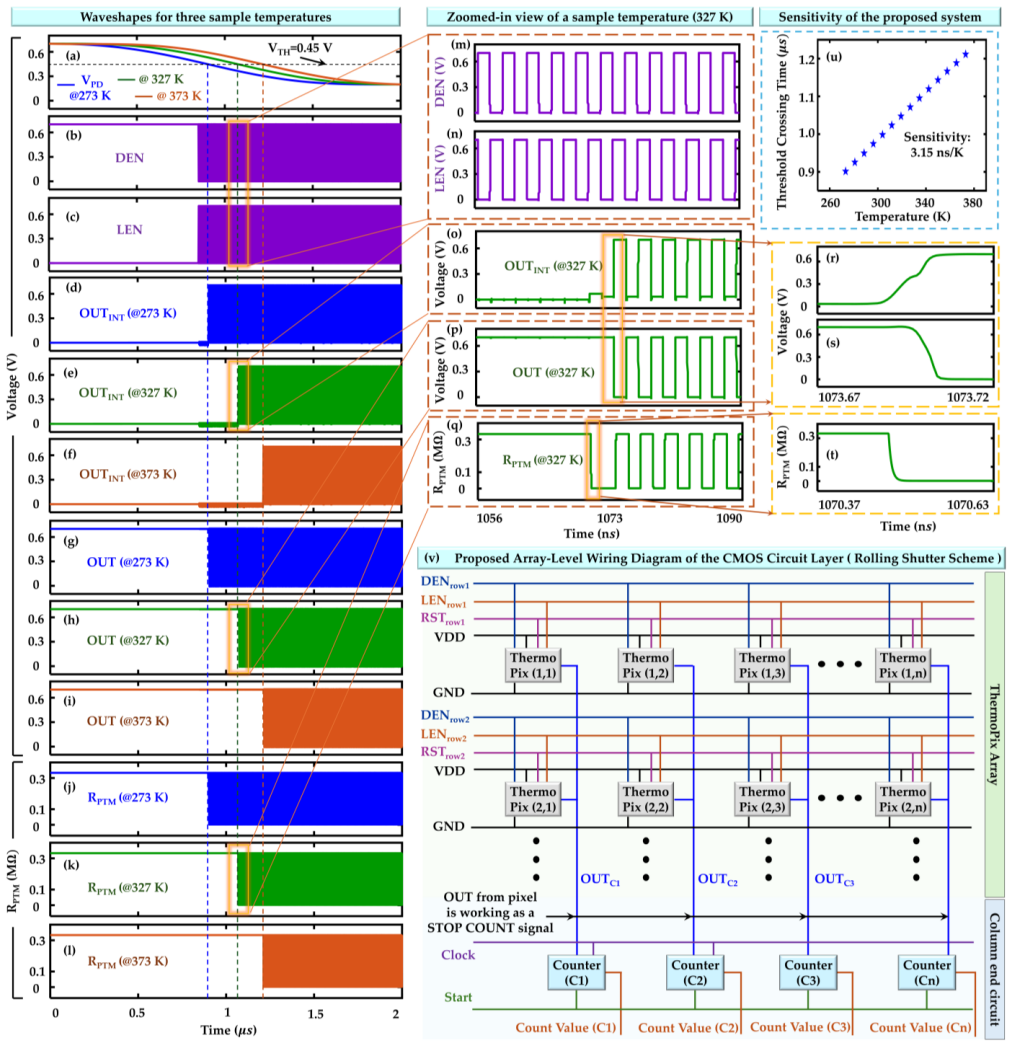
The central claim is that the VPCMZI's temperature-dependent spectral response, when detected by the integrated waveguide photodetector and translated into a time-varying photocurrent, can be used by a phase-transition-material device in CMOS to perform threshold detection and generate a timing signal corresponding to the temperature, achieving the reported performance metrics in simulations.
What carries the argument
The valley photonic crystal Mach-Zehnder interferometer (VPCMZI) that converts temperature to spectral shift, combined with photodetector and phase-transition-material CMOS threshold detector to produce timing output.
If this is right
- Temperature sensitivity reaches 3.15 ns/K.
- Row readout completes in 2 microseconds.
- Power-delay product is 0.152 fJ per sensing event.
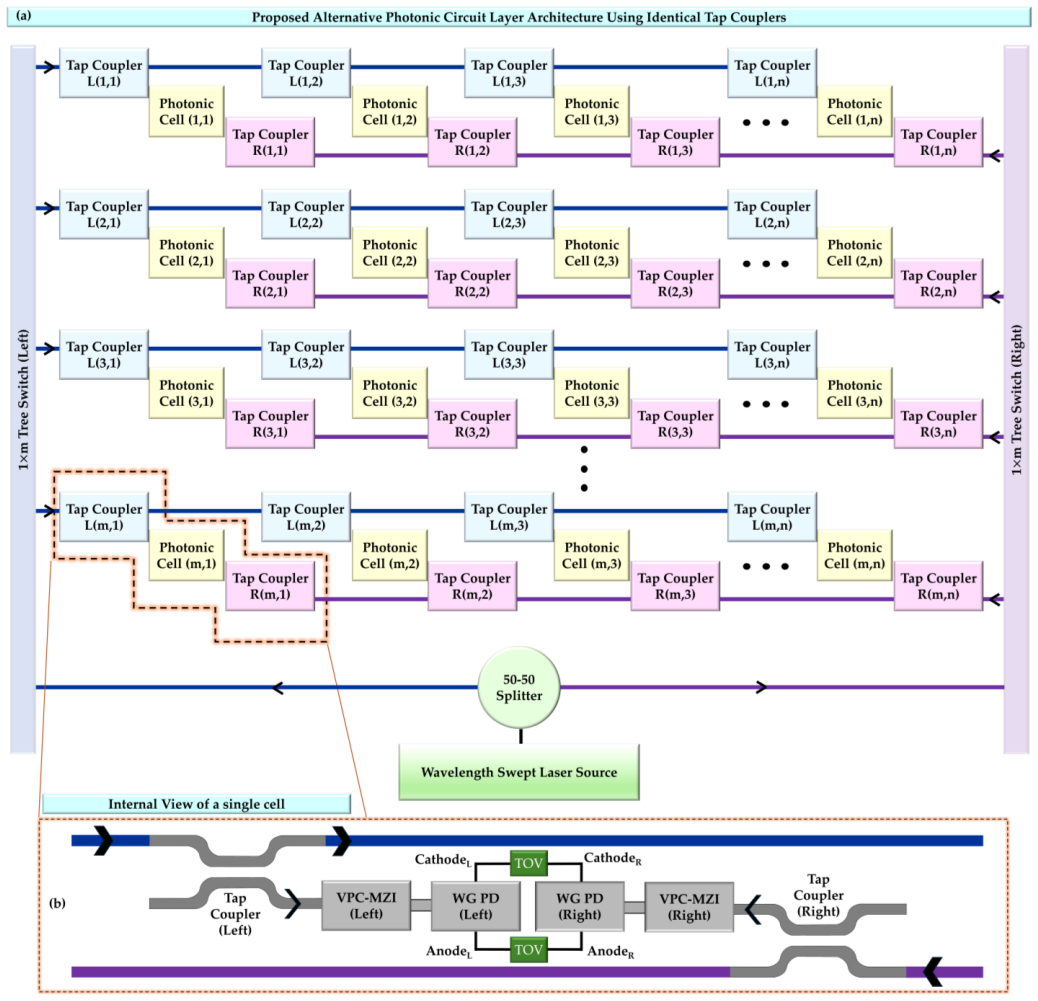
- Cell pitches can be 23.26 micrometers with varying tap ratios or 38.52 micrometers with bidirectional excitation.
- Optical power requirement is 150 nW per photonic cell.
Where Pith is reading between the lines
- This timing-based approach could reduce the need for complex analog circuitry in sensor arrays.
- The design may enable integration of temperature sensing directly into photonic-electronic chips for real-time thermal management.
- Power distribution schemes provide options for optimizing array density versus power uniformity.
- The method might extend to other parameters sensed via wavelength shifts in similar photonic structures.
Load-bearing premise
The temperature-dependent spectral response of the VPCMZI produces a clean time-varying photocurrent whose threshold crossing can be reliably detected by the phase-transition-material CMOS circuit without significant impact from noise or fabrication variation.
What would settle it
Fabrication and testing of a prototype array cell to measure the actual timing shift per Kelvin and observe if noise or variations cause unreliable threshold detections.
Figures
read the original abstract
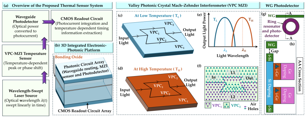
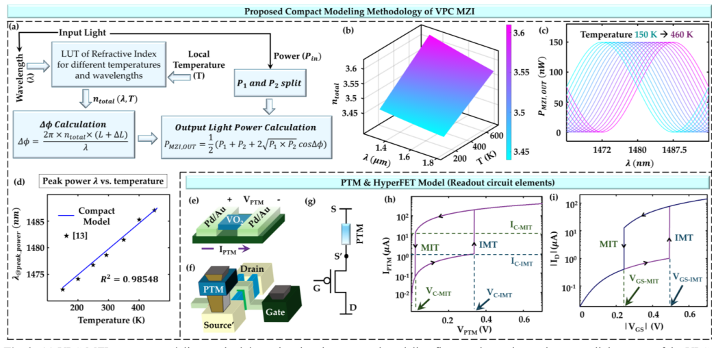
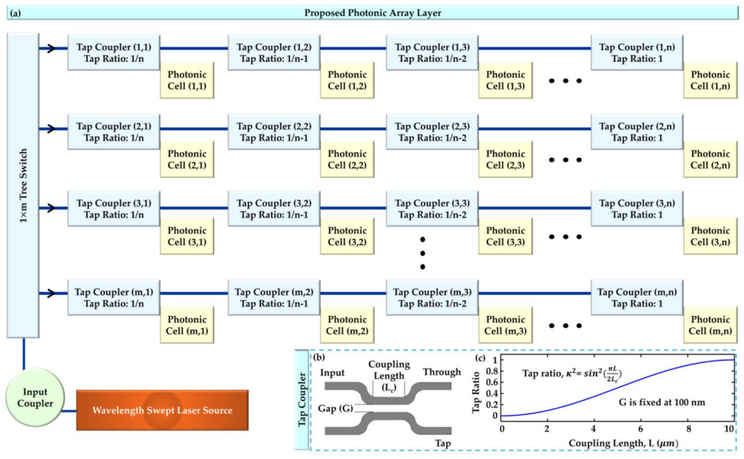
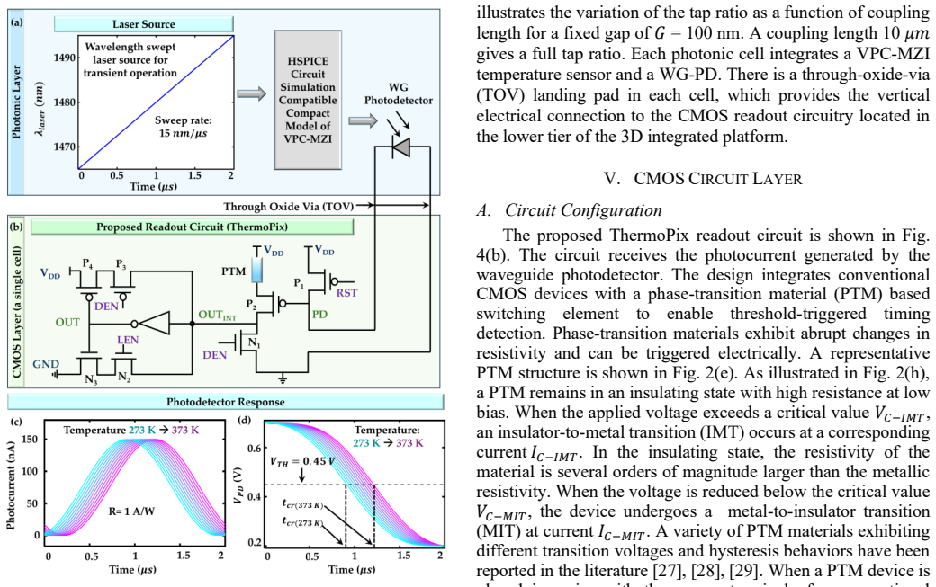
This paper presents ThermoPix, a CMOS-compatible electronic-photonic architecture for high-spatial-resolution temperature sensing. The proposed system converts temperature-induced wavelength shifts in a photonic interferometric sensor into timing information that can be processed by CMOS circuitry. We use a valley photonic crystal Mach-Zehnder interferometer (VPCMZI) as the sensing element, whose temperature-dependent spectral response is detected using an integrated waveguide photodetector and translated into a time-varying photocurrent. A CMOS readout circuit employing a phase-transition-material device performs threshold detection and generates a timing signal corresponding to the temperature-dependent crossing event. Circuit-level simulations demonstrate a temperature sensitivity of 3.15 ns/K, a row readout time of 2 us, and a sensing power-delay product (PDP) of 0.152 fJ. The required optical power per photonic cell is 150 nW, enabling energy-efficient array operation without requiring cooling or special environmental arrangements. We also present alternative photonic layer architectures for optical power distribution across the array. In one approach, we use different tap ratios along the row, while the other uses identical tap ratios with bidirectional excitation. The resulting average photonic cell pitches are 23.26 um and 38.52 um, respectively. The proposed ThermoPix architecture therefore provides a scalable platform for integrated temperature sensing arrays that combine photonic sensing elements with CMOS-compatible timing-based readout.
Editorial analysis
A structured set of objections, weighed in public.
Referee Report
Summary. The paper presents ThermoPix, a CMOS-compatible electronic-photonic architecture for high-spatial-resolution temperature sensing using a valley photonic crystal Mach-Zehnder interferometer (VPCMZI) whose temperature-dependent spectral response is detected by an integrated waveguide photodetector and converted to a timing signal via a phase-transition-material (PTM) CMOS readout circuit. Circuit-level simulations are reported to achieve 3.15 ns/K temperature sensitivity, 2 μs row readout time, 0.152 fJ sensing power-delay product (PDP), and 150 nW optical power per cell, along with two alternative photonic power-distribution schemes yielding average cell pitches of 23.26 μm and 38.52 μm.
Significance. If the simulation results hold under realistic conditions, the work could demonstrate a scalable, energy-efficient approach to integrating photonic temperature sensors with CMOS timing readout, enabling dense arrays without cooling or special environments and addressing needs for high-resolution thermal sensing in emerging-technology applications.
major comments (1)
- [Abstract and readout circuit paragraph] Abstract and readout-circuit paragraph: the reported metrics (3.15 ns/K sensitivity, 2 μs row readout, 0.152 fJ PDP) rest on circuit-level simulations of the VPCMZI spectral shift → waveguide-PD photocurrent → PTM threshold-crossing chain. No indication is given that these simulations include shot/thermal noise at the stated 150 nW optical power, fabrication-induced resonance variation, or PTM hysteresis/finite switching time; any of these could shift the effective crossing time by more than a few ns and render the sensitivity and PDP claims unreliable for array-scale operation.
Simulated Author's Rebuttal
We thank the referee for the careful review and for highlighting the assumptions underlying our circuit-level simulations. We address the major comment below and will revise the manuscript accordingly.
read point-by-point responses
-
Referee: [Abstract and readout circuit paragraph] Abstract and readout-circuit paragraph: the reported metrics (3.15 ns/K sensitivity, 2 μs row readout, 0.152 fJ PDP) rest on circuit-level simulations of the VPCMZI spectral shift → waveguide-PD photocurrent → PTM threshold-crossing chain. No indication is given that these simulations include shot/thermal noise at the stated 150 nW optical power, fabrication-induced resonance variation, or PTM hysteresis/finite switching time; any of these could shift the effective crossing time by more than a few ns and render the sensitivity and PDP claims unreliable for array-scale operation.
Authors: We agree that the reported metrics derive from ideal circuit-level simulations that do not incorporate shot/thermal noise at 150 nW, fabrication-induced resonance shifts, or PTM hysteresis and finite switching dynamics. These non-idealities are not modeled in the presented results, and their inclusion could indeed alter the effective timing precision. In the revised manuscript we will (1) explicitly state in the abstract and simulation sections that the metrics assume ideal conditions, (2) add a new subsection quantifying the expected impact of each effect using published device parameters, and (3) note that full noise-inclusive verification remains future work. This will clarify the scope of the claims without overstating the current simulation fidelity. revision: yes
Circularity Check
No circularity; simulation outputs are independent of fitted inputs
full rationale
The paper reports its headline metrics (3.15 ns/K sensitivity, 2 µs row readout, 0.152 fJ PDP) explicitly as outputs of circuit-level simulations of the VPCMZI spectral shift, waveguide PD photocurrent, and PTM threshold crossing. No equations, derivations, or parameter fits are shown that would make these quantities equivalent to their own inputs by construction. No self-citations, ansatzes smuggled via prior work, or uniqueness theorems are invoked to justify the architecture. The derivation chain is therefore self-contained against external simulation benchmarks rather than tautological.
Axiom & Free-Parameter Ledger
axioms (1)
- domain assumption Standard temperature-dependent refractive index shift in silicon photonic waveguides and ideal threshold behavior of phase-transition-material devices hold without significant process variation.
Reference graph
Works this paper leans on
-
[1]
Amusd: Asynchronous multi-device speculative decoding for llm acceleration
D. Lee and S. Kim, “A High -Speed and Compact On -Chip CMOS Temperature Sensor for 3D -NAND Flash Memory,” Proc. - IEEE Int. Symp. Circuits Syst., 2025, doi: 10.1109/ISCAS56072.2025.11043975
-
[2]
On-Chip Smart Temperature Sensors for Dark Current Compensation in CMOS Image Sensors,
S. Xie and A. J. P. Theuwissen, “On-Chip Smart Temperature Sensors for Dark Current Compensation in CMOS Image Sensors,” IEEE Sens. J. , vol. 19, no. 18, pp. 7849 –7860, Sep. 2019, doi: 10.1109/JSEN.2019.2919655
-
[3]
M. K. Sharma and B. Ramos -Alvarado, “Thermal management of 3 -D heterogeneously integrated microelectronics: challenges and future research directions,” Commun. Eng. 2026 51, vol. 5, no. 1, pp. 28 -, Feb. 2026, doi: 10.1038/s44172-026-00590-y
-
[4]
Reliability Assessment of Many -Core Dynamic Thermal Management,
A. Silva, I. Weber, A. L. D. M. Martins, and F. G. Moraes, “Reliability Assessment of Many -Core Dynamic Thermal Management,” Proc. - IEEE Int. Symp. Circuits Syst., vol. 2022-May, pp. 1590–1594, 2022, doi: 10.1109/ISCAS48785.2022.9937286
-
[5]
W. Shen et al., “Temperature imaging of chips with high spatiotemporal resolution using diamond nitrogen -vacancy centers,” Appl. Phys. Lett. , vol. 128, no. 9, p. 94001, Mar. 2026, doi: 10.1063/5.0305268
-
[6]
Printed temperature sensor array for high -resolution thermal mapping,
T. Bücher, R. Huber, C. Eschenbaum, A. Mertens, U. Lemmer, and H. Amrouch, “Printed temperature sensor array for high -resolution thermal mapping,” Sci. Reports 2022 121, vol. 12, no. 1, pp. 14231-, Aug. 2022, doi: 10.1038/s41598-022-18321-6
-
[7]
S. Lin et al., “District-scale surface temperatures generated from high - resolution longitudinal thermal infrared images,” Sci. Data 2023 101, vol. 10, no. 1, pp. 859-, Dec. 2023, doi: 10.1038/s41597-023-02749-0
-
[8]
W. Jeong, S. O. Kim, H. Lim, and K. Lee, “High -resolution thermal monitoring of lithium-ion batteries using Brillouin scattering based fiber optic sensor with flexible spatial arrangement of sensing points,” J. Energy Storage , vol. 104, no. 1, p. 114558, Dec. 2024, doi: 10.1016/j.est.2024.114558
-
[9]
L.-Y. Chiang, C. -T. Wang, T. -S. Lin, S. Pappert, and P. Yu, “Highly sensitive silicon photonic temperature sensor based on liquid crystal filled slot waveguide directional coupler,” Opt. Express, Vol. 28, Issue 20, pp. 29345-29356, vol. 28, no. 20, pp. 29345 –29356, Sep. 2020, doi: 10.1364/oe.403710
-
[10]
Physics-based models for photonic thermometers,
Z. Ahmed, “Physics-based models for photonic thermometers,” Sensors Actuators A Phys. , vol. 348, no. 16, p. 113987, Dec. 2022, doi: 10.1016/j.sna.2022.113987. TABLE II: Benchmarking Reference Sensor Type System Style Tech Node Readout / Conversion Time Sensitivity Energy / Power Metric Pixel Pitch
-
[11]
Time-domain CMOS sensor Electronic 0.18 µm 22.75 ms N/A FoM 6.7 pJ/K² N/A
-
[12]
MOS temperature sensor Electronic 0.18 µm 16 ms ±0.75 °C accuracy 36–40 µW 11 µm
-
[13]
Diode temperature sensor Electronic 0.35 µm ms-scale scan ~1 mV/K N/A ~250 µm
-
[14]
CMOS thermal sensor array Electronic 0.18 µm ms scale N/A N/A N/A
-
[15]
Photonic ring resonator Photonic 0.18 µm ~6 µs response 83 pm/°C N/A N/A ThermoPix (Approach I) Photonic thermal sensor array Electronic– photonic 3D 14 nm 2 µs row readout 3.15 ns/K 0.152 fJ PDP 23.26 µm ThermoPix (Approach II) Photonic thermal sensor array Electronic– photonic 3D 14 nm 2 µs row readout 3.15 ns/K 0.152 fJ PDP 38.52 µm 13
-
[16]
\ Bowers , author Michael \ Hochberg , author Richard \ Soref , \ and\ author Bhavin J
S. Shekhar et al. , “Roadmapping the next generation of silicon photonics,” Nat. Commun. 2024 151, vol. 15, no. 1, pp. 751-, Jan. 2024, doi: 10.1038/s41467-024-44750-0
-
[17]
A. H. El -Saeed et al. , “Low -Loss Silicon Directional Coupler With Arbitrary Coupling Ratios for Broadband Wavelength Operation Based on Bent Waveguides,” J. Light. Technol., vol. 42, no. 17, pp. 6011–6018, 2024, doi: 10.1109/JLT.2024.3407339
-
[18]
Design of a temperature sensor based on a valley photonic crystal Mach–Zehnder interferometer,
J. Bai et al., “Design of a temperature sensor based on a valley photonic crystal Mach–Zehnder interferometer,” Appl. Opt. Vol. 63, Issue 18, pp. 4940-4945, vol. 63, no. 18, pp. 4940 –4945, Jun. 2024, doi: 10.1364/ao.522148
-
[19]
G. G. E. Gielen, L. Hernandez, and P. Rombouts, “Time -Encoding Analog-to-Digital Converters: Bridging the Analog Gap to Advanced Digital CMOS?Part 2: Architectures and Circuits,” IEEE Solid -State Circuits Mag. , vol. 12, no. 3, pp. 18 –27, Jun. 2020, doi: 10.1109/MSSC.2020.3002144
-
[20]
Time -to-digital conversion techniques: a survey of recent developments,
J. Szyduczyński, D. Kościelnik, and M. Miśkowicz, “Time -to-digital conversion techniques: a survey of recent developments,” Measurement, vol. 214, no. 2, p. 112762, Jun. 2023, doi: 10.1016/j.measurement.2023.112762
-
[21]
Predictive first -principles simulations for co -designing next - generation energy-efficient AI systems,
D. Mamaluy, M. R. I. Udoy, J. P. Mendez, B. Feinberg, W. Pan, and A. Aziz, “Predictive first -principles simulations for co -designing next - generation energy-efficient AI systems,” Mar. 2026, Accessed: Mar. 16,
2026
-
[22]
Available: http://arxiv.org/abs/2603.08995
[Online]. Available: http://arxiv.org/abs/2603.08995
-
[23]
Sub-Micron Binary HyperPixel Sensor Circuit: In -Pixel Binarization with Variable Thresholding,
M. R. I. Udoy, M. M. Islam, A. Jaiswal, and A. Aziz, “Sub-Micron Binary HyperPixel Sensor Circuit: In -Pixel Binarization with Variable Thresholding,” 2024 IEEE Comput. Soc. Annu. Symp. VLSI , pp. 21–26, Jul. 2024, doi: 10.1109/ISVLSI61997.2024.00016
-
[24]
In -pixel foreground and contrast enhancement circuits with customizable mapping,
M. R. I. Udoy, M. M. Islam, E. Johnson, and A. Aziz, “In -pixel foreground and contrast enhancement circuits with customizable mapping,” Sci. Reports 2025 151, vol. 15, no. 1, pp. 1–10, Jan. 2025, doi: 10.1038/s41598-025-87965-x
-
[25]
C. Y. Zhu et al., “Two-dimensional semiconducting SnP2Se6 with giant second-harmonic-generation for monolithic on -chip electronic-photonic integration,” Nat. Commun. 2023 141 , vol. 14, no. 1, pp. 2521 -, May 2023, doi: 10.1038/s41467-023-38131-2
-
[26]
Demonstration of an optical chip-to-chip link in a 3D integrated electronic -photonic platform,
K. T. Settaluri et al., “Demonstration of an optical chip-to-chip link in a 3D integrated electronic -photonic platform,” Eur. Solid -State Circuits Conf., vol. 2015 -October, pp. 156 –159, Oct. 2015, doi: 10.1109/ESSCIRC.2015.7313852
-
[27]
Resonant Germanium -on-Silicon Photodetector with Evanescent Waveguide Coupling,
Z. Su et al. , “Resonant Germanium -on-Silicon Photodetector with Evanescent Waveguide Coupling,” Conf. Lasers Electro -Optics (2016), Pap. STh4E.4, p. STh4E.4, Jun. 2016, doi: 10.1364/cleo_si.2016.sth4e.4
-
[28]
B. Shi et al. , “Efficient coupling of topological photonic crystal waveguides based on transverse spin matching mechanism,” Nat. Commun. 2025 161 , vol. 16, no. 1, pp. 4645 -, May 2025, doi: 10.1038/s41467-025-59941-6
-
[29]
Refractive index of silicon and germanium and its wavelength and temperature derivatives,
H. H. Li, “Refractive index of silicon and germanium and its wavelength and temperature derivatives,” J. Phys. Chem. Ref. Data, vol. 9, no. 3, pp. 561–658, Jul. 1980, doi: 10.1063/1.555624
-
[30]
Integrating Atomistic Insights With Circuit Simulations via Transformer-Driven Symbolic Regression,
M. R. I. Udoy, J. Hutchins, S. Alam, C. Schuman, and A. Aziz, “Integrating Atomistic Insights With Circuit Simulations via Transformer-Driven Symbolic Regression,” IEEE J. Explor. Solid -State Comput. Devices Circuits , vol. 11, pp. 179 –187, 2025, doi: 10.1109/JXCDC.2025.3624662
-
[31]
Y. Fan et al. , “Ultra -Fast Broadband Wavelength -Swept DFB Laser Array with 400 kHz Sweep Rate and 60 nm Continuous Tuning Range,” ACS Photonics, Feb. 2026, doi: 10.1021/acsphotonics.5c01159
-
[32]
Z. Liang, Y. Shoji, and Y. Shoji, “All -optical remotely controllable 1 × 8 silicon thermo -optic switch based on Mach-Zehnder interferometers,” Opt. Express, Vol. 33, Issue 3, pp. 5539- 5550, vol. 33, no. 3, pp. 5539–5550, Feb. 2025, doi: 10.1364/oe.532245
-
[33]
A. Aziz, N. Shukla, S. Datta, and S. K. Gupta, “Steep switching hybrid phase transition FETs (Hyper-FET) for low power applications: A device- circuit co-design perspective - Part II,” IEEE Trans. Electron Devices , vol. 64, no. 3, pp. 1358 –1365, Mar. 2017, doi: 10.1109/TED.2017.2650598
-
[34]
Event Detection Pixel Sensor (EDPS) Circuit Using Phase Transition Material,
M. R. I. Udoy, C. Schuman, G. Rose, and A. Aziz, “Event Detection Pixel Sensor (EDPS) Circuit Using Phase Transition Material,” 2025 Device Res. Conf., pp. 1–2, Jun. 2025, doi: 10.1109/DRC66027.2025.11105748
-
[35]
A steep -slope transistor based on abrupt electronic phase transition,
N. Shukla et al. , “A steep -slope transistor based on abrupt electronic phase transition,” Nat. Commun. 2015 61 , vol. 6, no. 1, pp. 1 –6, Aug. 2015, doi: 10.1038/ncomms8812
-
[36]
Analysis of temperature dependence of Ge -on-Si p –i–n photodetectors,
M. Balbi, V. Sorianello, L. Colace, and G. Assanto, “Analysis of temperature dependence of Ge -on-Si p –i–n photodetectors,” Phys. E Low-dimensional Syst. Nanostructures , vol. 41, no. 6, pp. 1086 –1089, May 2009, doi: 10.1016/j.physe.2008.08.015
-
[37]
Predictive technology model for nano -CMOS design exploration,
W. Zhao and Y. Cao, “Predictive technology model for nano -CMOS design exploration,” ACM J. Emerg. Technol. Comput. Syst. , vol. 3, no. 1, Apr. 2007, doi: 10.1145/1229175.1229176;TAXONOMY:TAXONOMY:ACM- PUBTYPE;PAGEGROUP:STRING:PUBLICATION
work page doi:10.1145/1229175.1229176;taxonomy:taxonomy:acm- 2007
-
[38]
Device -Circuit Co -Design Employing Phase Transition Materials for Low Power Electronics,
A. Aziz and A. Dissertation, “Device -Circuit Co -Design Employing Phase Transition Materials for Low Power Electronics,” Aug. 2019, doi: 10.25394/PGS.8982722.V1
-
[39]
A Review of Digital Pixel Sensors,
M. R. I. Udoy, S. Alam, M. M. Islam, A. Jaiswal, and A. Aziz, “A Review of Digital Pixel Sensors,” IEEE Access, vol. 13, pp. 8533 –8551, 2025, doi: 10.1109/ACCESS.2025.3526879
-
[40]
Multidomain FeFET-Based Pixel for In-Sensor Multiply-and-Accumulate Operations,
M. R. I. Udoy, D. Ferrer, W. Li, K. Ni, and A. Aziz, “Multidomain FeFET-Based Pixel for In-Sensor Multiply-and-Accumulate Operations,” IEEE Trans. Electron Devices, 2025, doi: 10.1109/TED.2025.3615918
-
[41]
Z. Xu, X. Zhang, S. Chen, J. Cheong, and L. Yao, “A Temperature -to- Frequency Converter -Based On -Chip Temperature Sensor with an Inaccuracy of +0.65 °C/−0.49 °C,” Sensors 2023, Vol. 23, vol. 23, no. 11, May 2023, doi: 10.3390/s23115169
-
[42]
Diode temperature sensor array for measuring micro-scale surface temperatures with high resolution,
I. Y. Han and S. J. Kim, “Diode temperature sensor array for measuring micro-scale surface temperatures with high resolution,” Sensors Actuators A Phys. , vol. 141, no. 1, pp. 52 –58, Jan. 2008, doi: 10.1016/j.sna.2007.07.020
-
[43]
Miniaturized CMOS thermal sensor array for temperature gradient measurement in microprocessors,
K. Luria and J. Shor, “Miniaturized CMOS thermal sensor array for temperature gradient measurement in microprocessors,” ISCAS 2010 - 2010 IEEE Int. Symp. Circuits Syst. Nano -Bio Circuit Fabr. Syst. , pp. 1855–1858, 2010, doi: 10.1109/ISCAS.2010.5537829
-
[44]
G.-D. Kim et al., “Silicon photonic temperature sensor employing a ring resonator manufactured using a standard CMOS process,” Opt. Express, Vol. 18, Issue 21, pp. 22215 -22221, vol. 18, no. 21, pp. 22215 –22221, Oct. 2010, doi: 10.1364/oe.18.022215
discussion (0)
Sign in with ORCID, Apple, or X to comment. Anyone can read and Pith papers without signing in.