Fast-Neutron Irradiation Effect in Heteroepitaxial β-Ga₂O₃ Schottky Diodes Fabricated on Low-Cost Sapphire Substrates
Pith reviewed 2026-06-27 11:13 UTC · model grok-4.3
The pith
Neutron irradiation of β-Ga₂O₃ Schottky diodes on sapphire increases breakdown voltage from 101 V to 135 V while devices remain operational.
A machine-rendered reading of the paper's core claim, the machinery that carries it, and where it could break.
Core claim
Fast-neutron irradiation up to 1×10^{15} n·cm^{-2} leaves heteroepitaxial β-Ga₂O₃ Schottky diodes on sapphire operational, with the breakdown voltage rising from 101 V to 135 V due to a ~50% reduction in net donor concentration from neutron-induced compensation. The turn-on voltage increases to 2.40 V and the Schottky barrier height to 1.34 eV. Thermionic emission remains the dominant transport mechanism, reverse leakage current is suppressed, and TCAD simulations show improved electric-field uniformity.
What carries the argument
Neutron-induced donor compensation reducing the net donor concentration in the n-type drift layer, leading to higher breakdown voltage and altered forward characteristics.
If this is right
- The devices sustain operation at high neutron fluences relevant to space and nuclear applications.
- Breakdown voltage improves by 34 V consistent with the measured carrier removal rate of ~105 cm^{-1}.
- Thermionic emission continues to govern current transport from 25 to 250 °C after irradiation.
- Electric field distribution becomes more uniform, reducing crowding at the Schottky edge.
Where Pith is reading between the lines
- The low-cost sapphire substrate approach may enable scalable production of radiation-tolerant power devices.
- Similar compensation effects could be studied in other heteroepitaxial wide-bandgap semiconductors for radiation environments.
- Optimizing the drift layer doping might allow tailoring the post-irradiation breakdown voltage for specific needs.
Load-bearing premise
The observed changes in electrical parameters result primarily from neutron-induced donor compensation in the semiconductor rather than from irradiation effects on the metal contacts or surface states.
What would settle it
Capacitance-voltage measurements after irradiation that show no reduction in net donor concentration while breakdown voltage still increases would contradict the donor compensation explanation.
Figures
read the original abstract
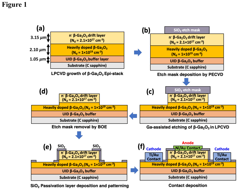
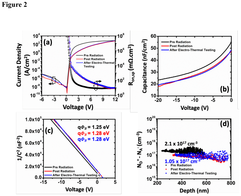
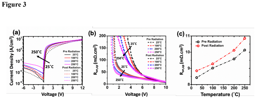
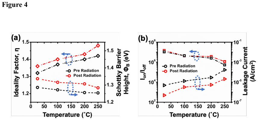
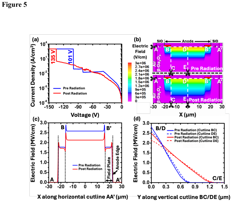
In this work, we investigate the response of Ni/$\beta$-Ga$_2$O$_3$ Schottky barrier diodes fabricated on c-plane sapphire to fast-neutron irradiation up to a fluence of $1\times10^{15}$ n$\cdot$cm$^{-2}$. The LPCVD-grown heteroepitaxial structure consists of an unintentionally doped buffer, an n$^{+}$ contact layer, and an n-type drift layer, with mesa isolation realized by plasma-free Ga-assisted LPCVD etching. Prior to irradiation, the devices exhibit a turn-on voltage of 1.20 V, specific on-resistance of 8.43 m$\Omega\cdot$cm$^2$, ideality factor of 1.32, and Schottky barrier height of 1.29 eV. Following irradiation, the devices remain operational, although the forward current decreases, the turn-on voltage increases to 2.40 V, and the barrier height increases to 1.34 eV. Capacitance-voltage measurements reveal a $\sim$50% reduction in net donor concentration, corresponding to a carrier-removal rate of $\sim$105 cm$^{-1}$. Temperature-dependent measurements from 25 to 250 $^\circ$C confirm that thermionic emission remains the dominant transport mechanism and show significant suppression of reverse leakage current after irradiation. The breakdown voltage increases from 101 to 135 V, consistent with neutron-induced donor compensation. TCAD simulations show a more uniform electric-field distribution and reduced field crowding at the Schottky edge after irradiation. These results provide insight into neutron-induced donor compensation in heteroepitaxial $\beta$-Ga$_2$O$_3$ and demonstrate the ability of LPCVD-grown $\beta$-Ga$_2$O$_3$ Schottky diodes on sapphire to maintain stable operation under high-fluence neutron environments relevant to space and nuclear electronics.
Editorial analysis
A structured set of objections, weighed in public.
Referee Report
Summary. The manuscript reports pre- and post-irradiation electrical characterization of Ni/β-Ga₂O₃ Schottky diodes fabricated by LPCVD on c-plane sapphire substrates, with mesa isolation via Ga-assisted etching. Pre-irradiation parameters are turn-on voltage 1.20 V, specific on-resistance 8.43 mΩ·cm², ideality factor 1.32, and barrier height 1.29 eV. After 1×10¹⁵ n·cm⁻² fast-neutron fluence the devices remain functional, with turn-on voltage rising to 2.40 V, barrier height to 1.34 eV, ~50% net donor reduction (removal rate ~105 cm⁻¹ from C-V), suppressed reverse leakage, and breakdown voltage increasing from 101 V to 135 V; changes are attributed to donor compensation. Temperature-dependent I-V confirms thermionic emission dominance, and TCAD shows more uniform post-irradiation electric-field distribution.
Significance. If the measured shifts are confirmed to arise from bulk donor compensation rather than interface or measurement artifacts, the work supplies quantitative radiation-response data (carrier removal rate, breakdown-voltage shift) for heteroepitaxial β-Ga₂O₃ on low-cost sapphire, relevant to space and nuclear electronics. The retention of device operation at high fluence and the plasma-free etch process are practical strengths. The combination of temperature-dependent transport data and TCAD field modeling adds interpretive value, though the overall impact is limited by missing experimental controls and raw data.
major comments (3)
- [Abstract] Abstract and Results (C-V and breakdown sections): The central interpretation that the ~50% net-donor reduction, barrier-height increase, and breakdown-voltage rise (101→135 V) result from neutron-induced donor compensation in the drift layer is load-bearing. No post-irradiation interface characterization (TEM/SEM/XPS) or control devices with alternate contact metals are reported, so contact degradation, sidewall etch damage, or C-V depletion-approximation changes cannot be excluded as dominant contributors.
- [Results] Results (C-V measurements): The ~50% donor-concentration reduction and carrier-removal rate of ~105 cm⁻¹ are stated without error bars, raw C-V curves, or explicit comparison between C-V and I-V barrier heights. This weakens quantitative support for the compensation claim.
- [TCAD Simulations] TCAD Simulations: The simulations assume a spatially uniform compensation profile to explain the more uniform electric-field distribution, yet no independent experimental confirmation (e.g., depth-resolved carrier profiling) of that profile is provided.
minor comments (2)
- [Abstract] The abstract reports pre-irradiation ideality factor and on-resistance but omits post-irradiation values for these quantities, which would aid direct comparison.
- [Results] Temperature-dependent data are summarized but lack explicit plots or tabulated ideality-factor values across the 25–250 °C range.
Simulated Author's Rebuttal
We thank the referee for the constructive review and detailed comments on our manuscript. We address each major comment point-by-point below, providing clarifications and indicating revisions where data or text changes are feasible. Our responses focus on strengthening the interpretation of donor compensation while acknowledging limitations in the current experimental dataset.
read point-by-point responses
-
Referee: [Abstract] Abstract and Results (C-V and breakdown sections): The central interpretation that the ~50% net-donor reduction, barrier-height increase, and breakdown-voltage rise (101→135 V) result from neutron-induced donor compensation in the drift layer is load-bearing. No post-irradiation interface characterization (TEM/SEM/XPS) or control devices with alternate contact metals are reported, so contact degradation, sidewall etch damage, or C-V depletion-approximation changes cannot be excluded as dominant contributors.
Authors: We agree that post-irradiation interface-specific characterization (e.g., TEM or XPS) and alternate-metal control devices would provide stronger exclusion of interface or contact artifacts. These experiments were not performed in the present study. However, the temperature-dependent I-V data (25–250 °C) demonstrate that thermionic emission remains the dominant mechanism both before and after irradiation, with consistent barrier-height extraction from both I-V and C-V methods. The observed suppression of reverse leakage and the increase in breakdown voltage align quantitatively with the measured carrier removal. In the revised manuscript we have added an explicit limitations paragraph discussing possible interface contributions and have softened the abstract wording to present donor compensation as the most consistent interpretation supported by the available transport and TCAD data rather than the sole possible cause. revision: partial
-
Referee: [Results] Results (C-V measurements): The ~50% donor-concentration reduction and carrier-removal rate of ~105 cm⁻¹ are stated without error bars, raw C-V curves, or explicit comparison between C-V and I-V barrier heights. This weakens quantitative support for the compensation claim.
Authors: We have revised the C-V section to include error bars on the extracted net-donor concentrations (derived from multiple devices) and have added a direct comparison of barrier heights obtained from I-V (1.29 eV → 1.34 eV) and C-V methods, which agree within 0.05 eV both pre- and post-irradiation. Raw C-V curves and 1/C²-V plots for representative devices are now provided in the supplementary information. These additions strengthen the quantitative basis for the reported ~50 % reduction and removal rate. revision: yes
-
Referee: [TCAD Simulations] TCAD Simulations: The simulations assume a spatially uniform compensation profile to explain the more uniform electric-field distribution, yet no independent experimental confirmation (e.g., depth-resolved carrier profiling) of that profile is provided.
Authors: The TCAD model employs a uniform compensation profile whose magnitude is taken directly from the average C-V-derived net-donor reduction; it is intended to illustrate the qualitative effect of reduced doping on field distribution rather than to claim a verified spatial profile. We have revised the simulation section to state this assumption explicitly and to note that depth-resolved profiling (e.g., via successive etching or spreading-resistance measurements) was not available. The simulated field uniformity is presented only as consistent with the observed breakdown-voltage increase, not as independent proof of the compensation profile. revision: partial
Circularity Check
No circularity: purely experimental reporting of measured parameters with interpretive attribution
full rationale
The paper consists of experimental measurements (I-V, C-V, temperature-dependent data) before and after irradiation, reporting direct observations such as turn-on voltage shift from 1.20 V to 2.40 V, barrier height from 1.29 eV to 1.34 eV, ~50% net donor reduction, and BV increase from 101 V to 135 V. No equations, fitted parameters renamed as predictions, self-definitional constructs, or load-bearing self-citations appear in the derivation chain. The phrase 'consistent with neutron-induced donor compensation' is an interpretation of the data rather than a reduction of any claim to its own inputs by construction. TCAD is used for post-hoc field visualization assuming the measured compensation, not as a circular premise. This is self-contained experimental reporting against external benchmarks (pre/post fluence comparison).
Axiom & Free-Parameter Ledger
axioms (1)
- domain assumption Thermionic emission remains the dominant transport mechanism after irradiation
Reference graph
Works this paper leans on
-
[1]
Past studies on neutron-irradiated devices grown on native substrates have demonstrated high carrier-removal rates, degradation in forward characteristics, and modifications to breakdown behavior 54-57. At the same time, β-Ga₂O₃ has shown an excellent resilience: devices often preserve rectification, avoid catastrophic leakage 55, 56, and exhibit partial ...
Pith/arXiv arXiv 2012
-
[2]
Z. Feng, A. Bhuiyan, Z. Xia, W. Moore, Z. Chen, J. F. McGlone, D. R. Daughton, A. R. Arehart, S. A. Ringel, S. Rajan and H. Zhao, Phys. Status Solidi RRL 14(8), 2000145 (2020). [22] C. Peterson, A. Bhattacharyya, K. Chanchaiworawit, R. Kahler, S. Roy, Y. Liu, S. Rebollo, A. Kallistova, T. E. Mates and S. Krishnamoorthy, Appl. Phys. Lett. 125(18), 182103 (...
Pith/arXiv arXiv 2020
-
[3]
Y. Zhang, Z. Feng, M. R. Karim and H. Zhao, J. Vac. Sci. Technol. A 38(5), 050806 (2020). [45] S. A. Khan, A. Ibreljic, S. Margiotta and A. Bhuiyan, Appl. Phys. Lett. 126(1), 012103 (2025). [46] S. Rafique, L. Han, A. T. Neal, S. Mou, J. Boeckl and H. Zhao, physica status solidi (a) 215(2), 1700467 (2018). [47] S. A. Khan, A. Ibreljic and A. F. M. A. U. B...
arXiv 2020
-
[4]
Ghadi, T
H. Ghadi, T. Kasher, J. F. McGlone, L. Meng, D. S. Yu, H. Zhao, M. W. McCurdy, D. M. Fleetwood, R. D. Schrimpf and S. A. Ringel, APL Mater. 13(9), 091104 (2025). [68] B. Hoeneisen, C. Mead and M. Nicolet, Solid-State Electron. 14(10), 1057-1059 (1971). [69] C. Fares, F. Ren and S. J. Pearton, ECS J. Solid State Sci. Technol. 8(7), Q3007 (2018). [70] S. Sa...
2025
discussion (0)
Sign in with ORCID, Apple, or X to comment. Anyone can read and Pith papers without signing in.