REVIEW 1 major objections 1 cited by
Mega: A 22 nm Convolutional Spiking Neural Network Accelerator Achieving 0.375 pJ/SOP for Efficient Edge Vision
T0 review · 1 major / 0 minor · reviewed 2026-06-30 · grok-4.3
Pith's one-line read Mega delivers 0.375 pJ per synaptic operation in a 22 nm convolutional SNN accelerator, four times better than prior designs.
desk verdict Mega reports a fabricated 22 nm SNN accelerator hitting 0.375 pJ/SOP with three practical architectural tweaks, but the abstract leaves measurement details thin. read the letter →
The pith
A machine-rendered reading of the paper's core claim, the machinery that carries it, and where it could break.
The reading
What carries the argument
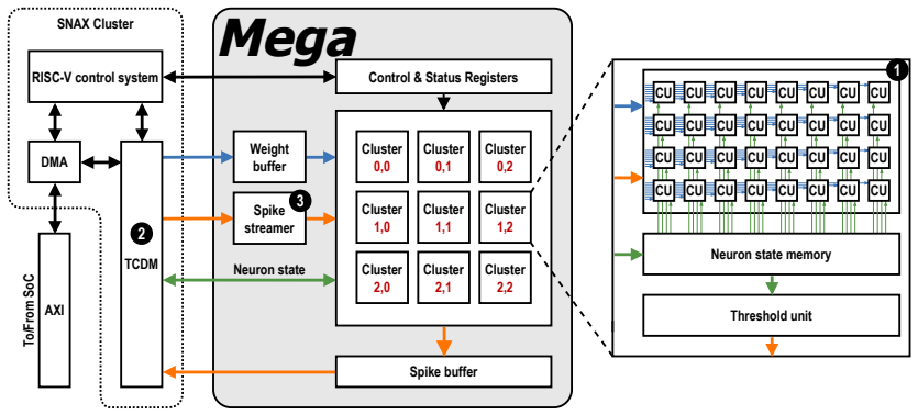
The combination of parallel 3×3 convolution engines, a single unified memory array for spikes/neuron states/weights, and low-overhead spike detection logic that together support varying layer sparsity and memory footprints.
What would settle it
Fabrication and measurement of Mega or an equivalent design in the same 22 nm process showing energy above 0.375 pJ/SOP or no 4× gain over the cited prior accelerators.
Extended reading notes
Core claim
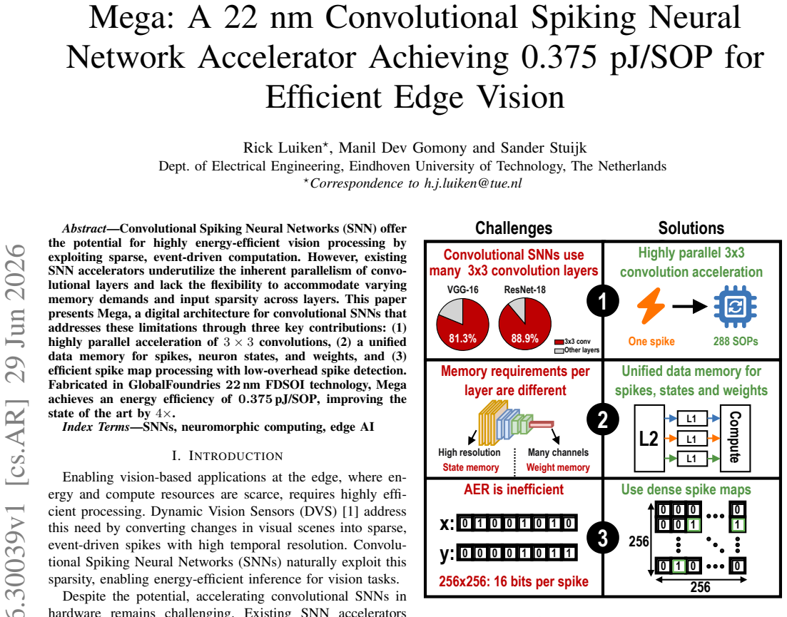
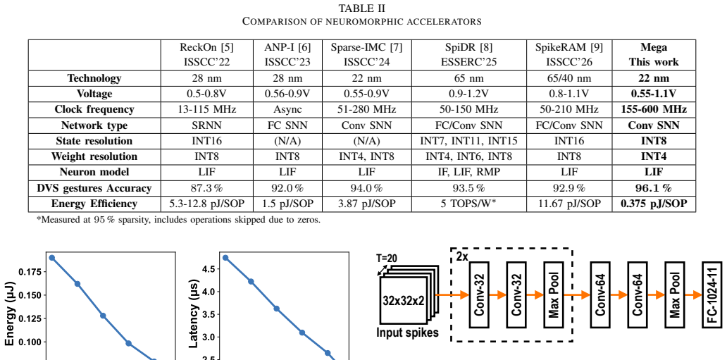
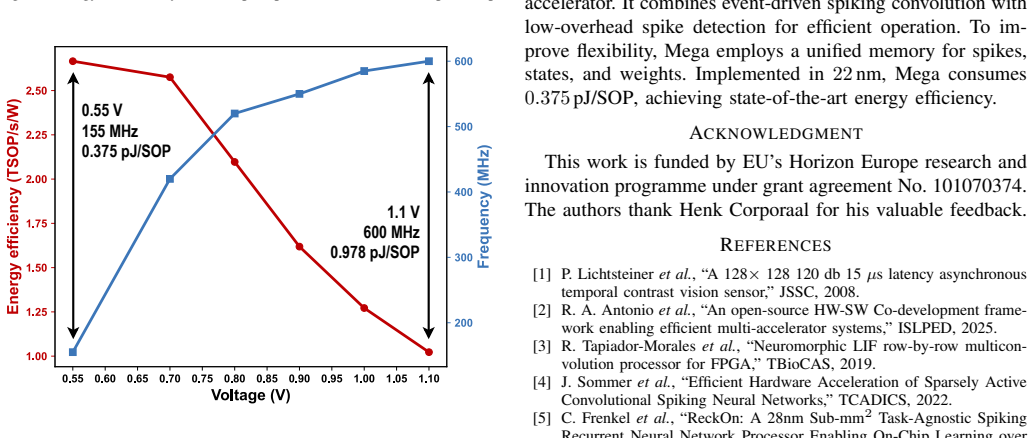
Mega is a digital architecture for convolutional SNNs that uses highly parallel acceleration of 3×3 convolutions, a unified data memory for spikes, neuron states, and weights, and efficient spike map processing with low-overhead spike detection. Fabricated in GlobalFoundries 22 nm FDSOI technology, it achieves an energy efficiency of 0.375 pJ/SOP, improving the state of the art by 4×.
Load-bearing premise
Existing SNN accelerators underutilize convolutional parallelism and cannot flexibly handle different memory demands and input sparsity across layers.
Editorial extensions
If this is right
- Convolutional layers can be processed with higher throughput per watt than in earlier SNN accelerators.
- A single memory structure suffices for spikes, states, and weights without separate banks for each.
- Spike detection overhead stays low enough to preserve the efficiency benefit of sparse event-driven computation.
- The measured 0.375 pJ/SOP figure holds across typical convolutional SNN vision workloads.
Reading between the lines
- The same memory-sharing and spike-handling ideas could be tested on networks that use larger or non-square kernels.
- End-to-end system power for a full camera-plus-classifier pipeline might drop further once the accelerator is paired with an event-based sensor.
- Designers of future edge chips could adopt the unified-memory pattern to reduce area overhead when supporting multiple data types.
Editorial analysis
A structured set of objections, weighed in public.
Referee Report
Summary. The paper presents Mega, a digital convolutional spiking neural network accelerator fabricated in GlobalFoundries 22 nm FDSOI technology. It identifies limitations in existing SNN accelerators regarding parallelism in convolutional layers and flexibility for varying memory and sparsity demands, then proposes three contributions: highly parallel acceleration of 3×3 convolutions, a unified data memory for spikes/neuron states/weights, and efficient spike map processing with low-overhead spike detection. The central result is a measured energy efficiency of 0.375 pJ/SOP, stated to improve the state of the art by 4×.
Significance. A well-documented post-fabrication measurement at this efficiency level, with transparent test conditions and comparisons, would represent a meaningful advance for energy-efficient edge vision hardware using convolutional SNNs, particularly by addressing underutilized parallelism and layer-specific flexibility.
major comments (1)
- [Abstract] Abstract: The central claim of 0.375 pJ/SOP energy efficiency (with 4× SOTA improvement) is presented without any details on test conditions, workload, baseline comparisons, error bars, or data exclusion criteria. This information is load-bearing for verifying the measured result on fabricated silicon.
Simulated Author's Rebuttal
We thank the referee for the constructive feedback and for recognizing the potential significance of our post-fabrication measurements. We respond point-by-point to the major comment below.
read point-by-point responses
-
Referee: [Abstract] Abstract: The central claim of 0.375 pJ/SOP energy efficiency (with 4× SOTA improvement) is presented without any details on test conditions, workload, baseline comparisons, error bars, or data exclusion criteria. This information is load-bearing for verifying the measured result on fabricated silicon.
Authors: We agree that the abstract would be strengthened by including concise context on the measurement conditions. The manuscript body (Sections 4 and 5) details the test setup, workload (specific convolutional SNN models and datasets for edge vision), baseline comparisons, and measurement methodology. To address this concern directly, we will revise the abstract to incorporate a brief statement on the workload and test conditions used to obtain the 0.375 pJ/SOP figure. revision: yes
Circularity Check
No significant circularity; central claim is post-fabrication measurement
full rationale
The paper reports a fabricated 22 nm FDSOI chip and its measured energy efficiency (0.375 pJ/SOP, 4× SOTA). The abstract and description list three architectural contributions at a high level but supply no equations, fitted parameters, derivations, or self-referential definitions. No load-bearing self-citations, ansatzes, or uniqueness theorems appear. The result is an empirical outcome from silicon, not a chain that reduces to its own inputs by construction.
Assumptions & free parameters
Cite this review
Pith. "Pith review of Mega: A 22 nm Convolutional Spiking Neural Network Accelerator Achieving 0.375 pJ/SOP for Efficient Edge Vision." pith.science (2026). https://pith.science/paper/XPEFWVB3
@misc{pith2026260630039,
  author       = {Pith},
  title        = {Pith review of: Mega: A 22 nm Convolutional Spiking Neural Network Accelerator Achieving 0.375 pJ/SOP for Efficient Edge Vision},
  year         = {2026},
  howpublished = {\url{https://pith.science/paper/XPEFWVB3}},
  note         = {Machine review of arXiv:2606.30039}
}
abstract
Convolutional Spiking Neural Networks (SNN) offer the potential for highly energy-efficient vision processing by exploiting sparse, event-driven computation. However, existing SNN accelerators underutilize the inherent parallelism of convolutional layers and lack the flexibility to accommodate varying memory demands and input sparsity across layers. This paper presents Mega, a digital architecture for convolutional SNNs that addresses these limitations through three key contributions: (1) highly parallel acceleration of $3 \times 3$ convolutions, (2) a unified data memory for spikes, neuron states, and weights, and (3) efficient spike map processing with low-overhead spike detection. Fabricated in GlobalFoundries 22 nm FDSOI technology, Mega achieves an energy efficiency of 0.375 pJ/SOP, improving the state of the art by $4\times$.
Figures
Figures from the paper (3 more)
Forward citations
Cited by 1 Pith paper
-
BitFair: A 12nm Bit-Serial CNN Accelerator with Learnable Early Termination and Adaptive Bit Ordering for Ultra-Low-Power XR Vision
A 12 nm bit-serial CNN accelerator with learnable ReLU early-termination thresholds and layer-wise adaptive bit ordering reaches 0.07 pJ/SOP and up to 117 BTOPS/W on XR vision tasks.
Reference graph
Works this paper leans on
-
[1]
A 128×128 120 db 15µs latency asynchronous temporal contrast vision sensor,
P. Lichtsteineret al., “A 128×128 120 db 15µs latency asynchronous temporal contrast vision sensor,” JSSC, 2008
2008
-
[2]
An open-source HW-SW Co-development frame- work enabling efficient multi-accelerator systems,
R. A. Antonioet al., “An open-source HW-SW Co-development frame- work enabling efficient multi-accelerator systems,” ISLPED, 2025
2025
-
[3]
Neuromorphic LIF row-by-row multicon- volution processor for FPGA,
R. Tapiador-Moraleset al., “Neuromorphic LIF row-by-row multicon- volution processor for FPGA,” TBioCAS, 2019
2019
-
[4]
Efficient Hardware Acceleration of Sparsely Active Convolutional Spiking Neural Networks,
J. Sommeret al., “Efficient Hardware Acceleration of Sparsely Active Convolutional Spiking Neural Networks,” TCADICS, 2022
2022
-
[5]
ReckOn: A 28nm Sub-mm 2 Task-Agnostic Spiking Recurrent Neural Network Processor Enabling On-Chip Learning over Second-Long Timescales,
C. Frenkelet al., “ReckOn: A 28nm Sub-mm 2 Task-Agnostic Spiking Recurrent Neural Network Processor Enabling On-Chip Learning over Second-Long Timescales,” ISSCC, 2022
2022
-
[6]
ANP-I: A 28nm 1.5pJ/SOP Asynchronous Spiking Neu- ral Network Processor Enabling Sub-0.1µJ/Sample On-Chip Learning for Edge-AI Applications,
J. Zhanget al., “ANP-I: A 28nm 1.5pJ/SOP Asynchronous Spiking Neu- ral Network Processor Enabling Sub-0.1µJ/Sample On-Chip Learning for Edge-AI Applications,” ISSCC, 2023
2023
-
[7]
A 22nm 0.26nW/Synapse Spike-Driven Spiking Neural Network Processing Unit Using Time-Step-First Dataflow and Sparsity- Adaptive In-Memory Computing,
Y . Liuet al., “A 22nm 0.26nW/Synapse Spike-Driven Spiking Neural Network Processing Unit Using Time-Step-First Dataflow and Sparsity- Adaptive In-Memory Computing,” ISSCC, 2024
2024
-
[8]
A 65nm 5 TOPS/W digital CIM accelerator with reconfigurable precision and temporal pipelining for spiking neural networks,
D. Sharmaet al., “A 65nm 5 TOPS/W digital CIM accelerator with reconfigurable precision and temporal pipelining for spiking neural networks,” ESSERC, 2025
2025
Show all 10 references
-
[9]
SpikeRAM: A 48.1pW/Synapse/Bit Event-Driven Spiking Compute-Near/In-Memory Processor with Neuromorphic Sensor En- abling Life-Long On-Chip Learning,
H. Fuet al., “SpikeRAM: A 48.1pW/Synapse/Bit Event-Driven Spiking Compute-Near/In-Memory Processor with Neuromorphic Sensor En- abling Life-Long On-Chip Learning,” ISSCC, 2026
2026
-
[10]
A low power, fully event-based gesture recognition system,
A. Amiret al., “A low power, fully event-based gesture recognition system,” CVPR, 2017
2017
Reviewed June 30, 2026 · model on record in the stance chip above.
Discussion (0). Sign in to comment.