REVIEW 3 major objections 5 minor 60 references
FPGA-Based Mini X-Ray Detector Front-End
T0 review · 3 major / 5 minor · reviewed 2026-07-15 · grok-4.5
Pith's one-line read A small FPGA pipeline can receive, store, detect, correct, and return synthetic X-ray-style pixel errors in real time.
desk verdict Solid course-project demo of a modular UART/BRAM/FSM image-correction pipeline; educational value is real, research novelty is not. read the letter →
The pith
A machine-rendered reading of the paper's core claim, the machinery that carries it, and where it could break.
The reading
What carries the argument
A top-level control FSM that arbitrates single-port BRAM ownership among the UART receive controller, image-processing core, UART transmit controller, and LCD logic so only one module drives memory at a time while the image core scans row-major, thresholds pixels, packs error coordinates, and writes corrected baselines.
What would settle it
Run the same dark and light test images through the board and check whether every deliberately injected error pixel is both counted on the LEDs, listed at the correct (x,y) on the LCD, and restored to the exact baseline value (10 or 180) in the returned image with no residual column shift or missed detections.
Extended reading notes
Core claim
The completed FPGA design successfully receives a 16×16 grayscale image over UART, stores it in BRAM, detects offset or gain-related pixel errors according to a selected mode, corrects those pixels, returns the corrected image to the host, shows the error count on LEDs, and lists stored error locations on an LCD, thereby proving a working proof-of-concept of the major detector-front-end pipeline steps.
Load-bearing premise
The claim rests on treating a few hand-placed defects in a tiny synthetic grayscale image, fixed numeric thresholds, and constant baseline replacement as enough to stand in for real detector offset and gain nonuniformity.
Editorial extensions
If this is right
- A modular UART–BRAM–FSM pipeline can demonstrate detector-style offset and gain correction without a physical X-ray sensor.
- Low resource use (under 0.5 % LUTs/FFs, half a BRAM block) leaves headroom for larger frames or extra defect types on the same Artix-7 board.
- Separate RX/TX controllers and a single clock domain keep serial transfer and image logic independently debuggable.
- Fixed-threshold correction plus LED/LCD feedback is enough for a controlled classroom proof-of-concept of front-end data flow.
Reading between the lines
- The same arbitration pattern could be reused for streaming larger frames if multi-ported or dual-buffer memory replaced the single-port BRAM.
- Replacing constant baselines with a short calibration-pass average would move the design closer to real flat-field correction without changing the outer FSM.
- The residual one-column shift points to a general lesson: synchronous BRAM latency must be pipeline-matched in any write-back image path.
Signed reviews
Editorial analysis
A structured set of objections, weighed in public.
Referee Report
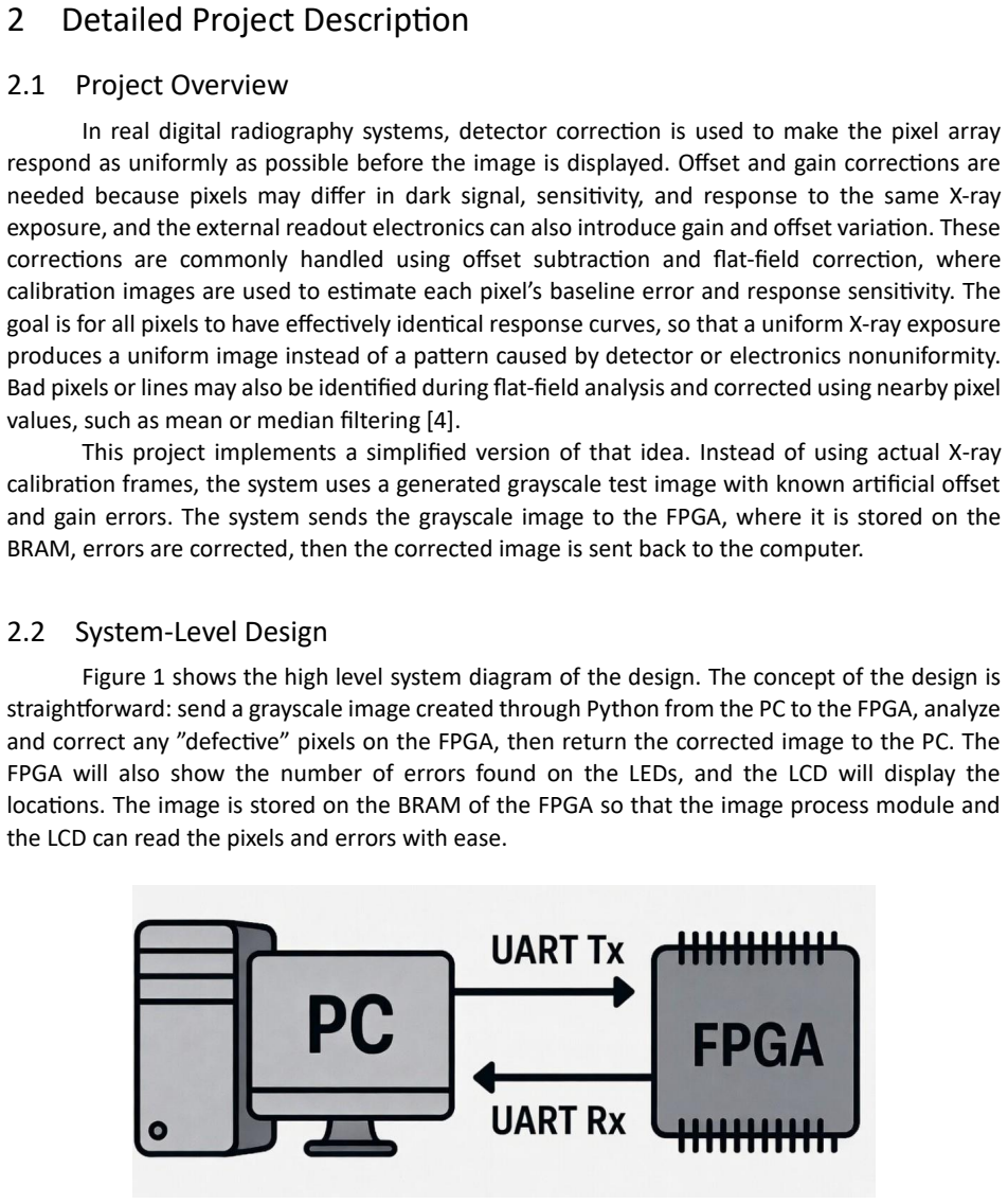
Summary. The manuscript presents a class-scale FPGA proof-of-concept for a simplified X-ray detector front-end on an Artix-7 AC701 board. A host Python script generates 16×16 grayscale test images with deliberately injected offset or gain defects, sends them over UART, and receives a corrected image. On the FPGA, a modular pipeline stores the frame in BRAM, uses a DIP-switch-selected mode to flag pixels against fixed dark/gain thresholds, replaces flagged pixels with constant baselines (10 or 180), stores error coordinates, returns the corrected frame, reports the error count on LEDs, and displays error locations on an LCD under button control. Implementation results report very low utilization, timing closure at 10 MHz, and successful detection of the injected defects in dark and light demos, with an acknowledged residual one-column shift in the returned light image attributed to BRAM latency.
Significance. As an educational demonstration of modular FPGA design for a medical-imaging-inspired pipeline (UART, BRAM arbitration, image-processing FSM, LCD feedback), the work is useful and the hardware demos (Figures 8–9, Tables 2–3) and resource/timing numbers are concrete. It does not claim a new detector-correction algorithm or transfer to real flat-field calibration; the contribution is a working, documented student-scale system that separates communication, memory ownership, and correction. That limited claim is supported by the reported demos. The long closing citation block to the same research group does not add technical novelty to the pipeline itself.
major comments (3)
- The manuscript is written as a course final-project report (motivation from lab experience, class LCD notes [5], “bonus” LCD, residual bugs left for future work) rather than a research article. For a serious cs.AR journal, the central claim is only a working 16×16 synthetic demo; there is no comparison to prior FPGA front-ends beyond brief citations, no quantitative latency/throughput analysis of the pipeline, and no evaluation against real detector data or standard flat-field methods. Without a clear research question and baseline comparison, the work does not meet typical archival standards even if the demo is correct.
- Section 3.1.3 and 4.1.2–4.1.3: correction is fixed-threshold flagging plus replacement by constant baselines (dark=10, light=180). Exact threshold values are never stated, and no calibration-frame or per-pixel gain-map path is implemented. The authors acknowledge this as a simplification (Sections 1.2, 2.1, 4.2), but the abstract and introduction still frame the work as a mini X-ray detector front-end. Either the claim language must be narrowed strictly to “synthetic threshold demo” or a more representative correction path (or at least explicit thresholds and sensitivity analysis) is needed for the medical-imaging framing to hold.
- Section 4.1.3 reports a residual one-column shift in the returned light image, attributed to BRAM read latency / FSM alignment, and Section 3.3 notes remaining latency issues. Because the strongest claim (Section 4.3) includes returning a correctly ordered corrected image, this is a load-bearing functional defect for the output path. A fix (explicit address/data pipelining or corrected write-back/TX sequencing) or a clear demonstration that the shift is eliminated should be required before acceptance of the pipeline claim.
minor comments (5)
- Abstract and Section 1.1 largely repeat the same medical-imaging motivation paragraph; tighten and state the concrete 16×16 UART–BRAM–correct–return scope up front.
- Figures 1–9 are referenced but not available as high-resolution captions with signal names; ensure waveforms (Figures 3–6) label key signals (process_start, bram_we, error_count, etc.) so the simulations are reproducible from the text alone.
- References [6]–[59] are almost entirely from one research group and are used mainly to assert that FPGAs are generally suitable; prune to works that directly inform detector front-ends, flat-field correction, or the specific architecture choices.
- Table 1 and peripheral description are clear; add the exact dark/high-gain/low-gain threshold constants and BRAM address map (image 0–255, error list from 256) in a small table for reproducibility.
- Minor typos and formatting: “frontend”/“front-end” inconsistency, “image process core” vs “image-processing,” and incomplete DOI/URL punctuation in the reference list.
Circularity Check
No derivation circularity: the demo is a self-contained synthetic pipeline; only a non-load-bearing self-citation block frames FPGAs as 'best option'.
-
self citation load bearing
[Section 4.3 closing paragraphs; refs [6]–[59]]
"This work is inspired by the digital design research group at UCCS. This group has done extensive work in FPGA-based architectures, techniques, and associated models. Their analyses [6],[7] show that FPGA-based embedded systems are currently the best option to support applications and techniques, such as the ones presented in this report. Also, their previous work on FPGA-based embedded accelerators... demonstrated that FPGA-based embedded systems are the best avenue to support and accelerate complex algorithms and techniques."
The claim that FPGAs are 'the best option/avenue' for this class of system is justified almost entirely by a long chain of self-group citations rather than by independent external benchmarks or by the demo itself. The demo result (working synthetic pipeline) does not depend on that ranking, so the circularity is framing-only and not load-bearing for the paper's strongest claim.
full rationale
This is an educational FPGA proof-of-concept, not a first-principles derivation paper. The strongest claim (Section 4.3) is that a modular design received a 16×16 grayscale image over UART, stored it in BRAM, detected offset/gain errors via fixed thresholds, corrected pixels to constant baselines (10 or 180), returned the image, and displayed error count/locations on LEDs/LCD. Those steps are verified by construction against deliberately injected defects (Tables 2–3, Figures 8–9) and by simulation/implementation results; they do not reduce to a fitted parameter renamed as prediction, nor to a uniqueness theorem. The authors explicitly scope the work as a simplified class demo (Sections 1.2, 2.1), not a commercial detector. The only mild circularity-adjacent pattern is the closing block (end of Section 4.3 and refs [6]–[59]), almost all from the same group, used to assert that FPGA-based embedded systems are 'the best option' and to list future optimization directions. That framing is not load-bearing for the reported pipeline result, so the score remains 1 rather than 0.
Assumptions & free parameters
free parameters (5)
- dark baseline correction value =
10
- light baseline correction value =
180
- dark / high-gain / low-gain thresholds =
unspecified
- image size and BRAM layout =
16×16 / 256-pixel image region
- system clock and UART baud =
10 MHz / 9600 baud
assumptions (3)
- domain assumption Offset and gain nonuniformity in a real X-ray detector can be adequately represented by a few pixels that simply exceed or fall below fixed grayscale thresholds on a synthetic dark or light frame.
- domain assumption A single-port BRAM can be safely time-multiplexed among RX, image processor, TX, and LCD by a top-level FSM without data corruption provided only one master is enabled per state.
- ad hoc to paper Replacing a flagged pixel by a constant baseline is a valid stand-in for offset subtraction and flat-field gain correction used in commercial detectors.
Cite this review
Pith. "Pith review of FPGA-Based Mini X-Ray Detector Front-End." pith.science (2026). https://pith.science/paper/N5SAGJOB
@misc{pith2026260712126,
  author       = {Pith},
  title        = {Pith review of: FPGA-Based Mini X-Ray Detector Front-End},
  year         = {2026},
  howpublished = {\url{https://pith.science/paper/N5SAGJOB}},
  note         = {Machine review of arXiv:2607.12126}
}
read the original abstract
Medical imaging systems require reliable front-end electronics that can acquire sensor data, process image information, identify errors, and communicate results to other parts of the system. In applications such as X-ray imaging, CT, PET, ultrasound, and other diagnostic imaging systems, the electronics must often handle large amounts of data while maintaining predictable timing and low-latency operation. Because of these requirements, FPGAs (Field Programmable Gate Arrays) are commonly useful for medical imaging and signal-processing applications. In this project, the medical imaging concept is simplified into a small FPGA-based frontend demonstration.
Figures


Figures from the paper (6 more)


Reference graph
Works this paper leans on
-
[6]
D. G. Perera, Lecture 6: Homework 5: Lcd, Lecture slides for ECE 4211/5211: Rapid Prototyping with FPGAs, University of Colorado Colorado Springs, Course materials, 2026
2026
-
[59]
An Efficient FPGA-Based Memory Architecture for Compute-Intensive Applications on Embedded Devices
S.N. Shahrouzi and D.G. Perera, “An Efficient FPGA-Based Memory Architecture for Compute-Intensive Applications on Embedded Devices”, in Proceedings of the IEEE Pacific Rim International Conference on Communications, Computers, and Signal Processing, (PacRim’17), pp. 1-8, Victoria, BC, Canada, August 2017
2017
-
[5]
Yorkston, Design and performance characteristics of flat-panel acquisition technologies, AAPM presentation, American Association of Physicists in Medicine
J. Yorkston, Design and performance characteristics of flat-panel acquisition technologies, AAPM presentation, American Association of Physicists in Medicine. [Online]. Available: https://www.aapm.org/meetings/amos2/pdf/26- 5957-59342-727.pdf
-
[1]
Fpga-based front-end electronics for positron emission tomography,
M. Haselman, R. S. Miyaoka, T. K. Lewellen, S. Hauck, W. McDougald, and D. DeWitt, “Fpga-based front-end electronics for positron emission tomography,” IEEE Transactions on Nuclear Science, vol. 56, no. 1, pp. 31–35,
-
[2]
DOI: 10.1109/TNS.2008.2008751)
-
[3]
Yadav, What is an fpga and how is it transforming medical devices? KritiKal Solutions, May 2025
S. Yadav, What is an fpga and how is it transforming medical devices? KritiKal Solutions, May 2025. [Online]. Available: https://kritikalsolutions.com/what-isan-fpga-and-how-is-it-transforming-medical-devices/)
2025
-
[4]
[Online]
VLSI First, Medical imaging and signal processing: Advancements enabled by fpga design, VLSI First, 2025. [Online]. Available: https://vlsifirst.com/blog/medicalimaging-and-signal-processing-by-fpga-design
2025
-
[7]
Analysis of Single-Chip Hardware Support for Mobile and Embedded Applications,
D.G. Perera and K.F. Li, "Analysis of Single-Chip Hardware Support for Mobile and Embedded Applications," in Proc. of IEEE Pacific Rim Int. Conf. on Communication, Computers, and Signal Processing, (PacRim’13), pp. 369 - 376, Victoria, BC, Canada, August 2013
2013
Show all 60 references
-
[8]
Analysis of Computation Models and Application Characteristics Suitable for Reconfigurable FPGAs
D.G. Perera and K.F. Li, “Analysis of Computation Models and Application Characteristics Suitable for Reconfigurable FPGAs”, in Proc. of 10th IEEE Int. Conf. on P2P, Parallel, Grid, Cloud, and Internet Computing, (3PGCIC’15), pp. 244-247, Krakow, Poland, Nov. 2015
2015
-
[9]
Optimized Hardware Accelerators for Data Mining Applications on Embedded Platform: Case Study Principal Component Analysis,
S.N. Shahrouzi and D.G. Perera, "Optimized Hardware Accelerators for Data Mining Applications on Embedded Platform: Case Study Principal Component Analysis," Elsevier Journal on Microprocessor and Microsystems (MICPRO), vol. 65, pp. 79-96, March 2019
2019
-
[10]
Embedded Hardware Solution for Principal Component Analysis,
D.G. Perera and K.F. Li, "Embedded Hardware Solution for Principal Component Analysis," in Proc. of IEEE Pacific Rim Int. Conf. on Communication, Computers, and Signal Processing, (PacRim’11), pp.730 -735, Victoria, BC, Canada, August 2011
2011
-
[11]
Hardware Acceleration for Similarity Computations of Feature Vectors,
D.G. Perera and Kin F. Li, “Hardware Acceleration for Similarity Computations of Feature Vectors,” IEEE Canadian Journal of Electrical and Computer Engineering, (CJECE), vol. 33, no. 1, pp. 21 -30, Winter 2008
2008
-
[12]
On-Chip Hardware Support for Similarity Measures,
D.G. Perera and K.F. Li, “On-Chip Hardware Support for Similarity Measures,” in Proc. of IEEE Pacific Rim Int. Conf. on Communication, Computers, and Signal Processing, (PacRim’07), pp. 354 -358, Victoria, BC, Canada, August 2007
2007
-
[13]
An Investigation of Chip-Level Hardware Support for Web Mining,
K.F. Li and D.G. Perera, “An Investigation of Chip-Level Hardware Support for Web Mining,” in Proc. of IEEE Int. Symp. on Data Mining and Information Retrieval, (DMIR’07), pp. 341 -348, Niagara Falls, ON, Canada, May 2007
2007
-
[14]
A Hardware Collective Intelligent Agent
K.F. Li and D.G. Perera, “A Hardware Collective Intelligent Agent”, Transactions on Computational Collective Intelligence, LNCS 7776, Springer, pp. 45-59, 2013
2013
-
[15]
Optimizing Density-Based Ant Colony Stream Clustering Using FPGA-Based Hardware Accelerator
J.R. Graf and D.G. Perera, “Optimizing Density-Based Ant Colony Stream Clustering Using FPGA-Based Hardware Accelerator”, in Proc. Of IEEE Int. Symp. on Circuits and Systems (ISCAS’23), 5 -page manuscript, Monterey, California, May 2023
2023
-
[16]
Chip-Level and Reconfigurable Hardware for Data Mining Applications,
D.G. Perera, “Chip-Level and Reconfigurable Hardware for Data Mining Applications,” PhD Dissertation, Department of Electrical & Computer Engineering, University of Victoria, Victoria, BC, Canada, April 2012
2012
-
[17]
Optimized Embedded and Reconfigurable Hardware Architectures and Techniques for Data Mining Applications on Mobile Devices
S. Navid Shahrouzi, "Optimized Embedded and Reconfigurable Hardware Architectures and Techniques for Data Mining Applications on Mobile Devices", PhD Dissertation, Department of Electrical & Computer Engineering, University of Colorado Colorado Springs, December 2018
2018
-
[18]
Optimizing Density-Based Ant Colony Stream Clustering Using FPGAs
J. Graf, "Optimizing Density-Based Ant Colony Stream Clustering Using FPGAs", MSc Thesis, Department of Electrical & Computer Engineering, University of Colorado Colorado Springs, CO, USA, March 2022
2022
-
[19]
Efficient Embedded Architectures for Model Predictive Controller for Battery Cell Management in Electric Vehicles
A.K. Madsen and D.G. Perera, “Efficient Embedded Architectures for Model Predictive Controller for Battery Cell Management in Electric Vehicles”, EURASIP Journal on Embedded Systems, SpringerOpen, vol. 2018, article no. 2, 36-page manuscript, July 2018. 18
2018
-
[20]
An Optimized FPGA-Based Hardware Accelerator for Physics- Based EKF for Battery Cell Management
A.K. Madsen, M.S. Trimboli, and D.G. Perera, “An Optimized FPGA-Based Hardware Accelerator for Physics- Based EKF for Battery Cell Management”, in Proc. of IEEE Int,l Symp, on Circuits and Systems, (ISCAS’20), 5 -page manuscript, Seville, Spain, May 2020
2020
-
[21]
Towards Composing Efficient FPGA-Based Hardware Accelerators for Physics- Based Model Predictive Control Smart Sensor for HEV Battery Cell Management
A.K. Madsen and D.G. Perera, “Towards Composing Efficient FPGA-Based Hardware Accelerators for Physics- Based Model Predictive Control Smart Sensor for HEV Battery Cell Management”, IEEE ACCESS, (Open Access Journal in IEEE), pp. 106141-106171, 25th September 2023
2023
-
[22]
Composing Optimized Embedded Software Architectures for Physics -Based EKF- MPC Smart Sensor for Li-Ion Battery Cell Management
A.K. Madsen and D.G. Perera, “Composing Optimized Embedded Software Architectures for Physics -Based EKF- MPC Smart Sensor for Li-Ion Battery Cell Management”, Sensors, MDPI open access journal, Intelligent Sensors Section, 21-page manuscript, vol. 22, no. 17, 26th August 2022
2022
-
[23]
Optimized Embedded Architectures for Model Predictive Control Algorithms for Battery Cell Management Systems in Electric Vehicles
A.K. Madsen, “Optimized Embedded Architectures for Model Predictive Control Algorithms for Battery Cell Management Systems in Electric Vehicles”; PhD Dissertation, Department of Electrical & Computer Engineering, University of Colorado Colorado Springs, August 2020
2020
-
[24]
An FPGA-Based Linear Kalmann Filter for a Two-Phase Buck Converter Application
D. Abillar, "An FPGA-Based Linear Kalmann Filter for a Two-Phase Buck Converter Application", MSc Thesis, Department of Electrical & Computer Engineering, University of Colorado Colorado Springs, CO, USA, April 2024
2024
-
[25]
Efficient FPGA-Based Reconfigurable Accelerators for SIMON Cryptographic Algorithm on Embedded Platforms
A. Alkamil and D.G. Perera, “Efficient FPGA-Based Reconfigurable Accelerators for SIMON Cryptographic Algorithm on Embedded Platforms”, in Proceedings of the IEEE International Conferences on Reconfigurable Computing and FPGAs, (ReConFig’19), 8-page manuscript, Cancun, Mexico,...
2019
-
[26]
Towards Dynamic and Partial Reconfigurable Hardware Architectures for Cryptographic Algorithms on Embedded Devices
A. Alkamil and D.G. Perera, “Towards Dynamic and Partial Reconfigurable Hardware Architectures for Cryptographic Algorithms on Embedded Devices”, IEEE Access, Open Access Journal in IEEE, vol. 8, pp: 221720 – 221742, 10th December 2020
2020
-
[27]
Dynamic Reconfigurable Architectures to Improve Performance and Scalability of Cryptosystems on Embedded Systems
A. Alkamil, “Dynamic Reconfigurable Architectures to Improve Performance and Scalability of Cryptosystems on Embedded Systems”, PhD Dissertation, Department of Electrical & Computer Engineering, University of Colorado Colorado Springs, 5th February 2021
2021
-
[28]
An FPGA-Based Hardware Accelerator for K-Nearest Neighbor Classification for Machine Learning on Mobile Devices
M.A. Mohsin and D.G. Perera, “An FPGA-Based Hardware Accelerator for K-Nearest Neighbor Classification for Machine Learning on Mobile Devices”, in Proceedings of the IEEE/ACM International Symposium on Highly Efficient Accelerators and Reconfigurable Technologies, (HEART’18), ...
2018
-
[29]
An Efficient FPGA-Based Hardware Accelerator for Convex Optimization-Based SVM Classifier for Machine Learning on Embedded Platforms
S. Ramadurgam and D.G. Perera, “An Efficient FPGA-Based Hardware Accelerator for Convex Optimization-Based SVM Classifier for Machine Learning on Embedded Platforms”, Electronics, MDPI open access journal, 36 -page manuscript, vol. 10, no. 11, 31st May 2021
2021
-
[30]
A Systolic Array Architecture for SVM Classifier for Machine Learning on Embedded Devices
S. Ramadurgam and D.G. Perera, “A Systolic Array Architecture for SVM Classifier for Machine Learning on Embedded Devices”, in Proc. of IEEE Int. Symp. on Circuits and Systems (ISCAS’23), 5 -page manuscript, Monterey, California, May 2023
2023
-
[31]
FPGA -based Hardware Accelerator for Bottleneck Residual Blocks of MobileNetV2 Convolutional Neural Networks
Jordi P. Miró, Mokhles A. Mohsin, Arkan Alkamil and Darshika G. Perera, “FPGA -based Hardware Accelerator for Bottleneck Residual Blocks of MobileNetV2 Convolutional Neural Networks”, in Proceedings of the IEEE Mid -West Symposium on Circuits and Systems (MWCAS’25), 5-page man...
2025
-
[32]
An FPGA-Based Hardware Accelerator for K-Nearest Neighbor Classification for Machine Learning
M. A. Mohsin, "An FPGA-Based Hardware Accelerator for K-Nearest Neighbor Classification for Machine Learning", MSc Thesis, Department of Electrical & Computer Engineering, University of Colorado Colorado Springs, CO, USA, December 2017
2017
-
[33]
Optimized Embedded Architectures and Techniques for Machine Learning Algorithms for On -Chip AI Acceleration
S. Ramadurgam, “Optimized Embedded Architectures and Techniques for Machine Learning Algorithms for On -Chip AI Acceleration”, PhD Dissertation, Department of Electrical & Computer Engineering, University of Colorado Colorado Springs, 12th February 2021
2021
-
[34]
FPGA-Based Accelerators for Convolutional Neural Networks on Embedded Devices
J. P. Miro, " FPGA-Based Accelerators for Convolutional Neural Networks on Embedded Devices", MSc Thesis, Department of Electrical & Computer Engineering, University of Colorado Colorado Springs, CO, USA, May 2020
2020
-
[35]
An Efficient Hardware Accelerator for Binary Residual Neural Network Using FPGAs
R. Wallace, "An Efficient Hardware Accelerator for Binary Residual Neural Network Using FPGAs ", MSc Thesis, Department of Electrical & Computer Engineering, University of Colorado Colorado Springs, CO, USA, May 2026
2026
-
[36]
Intelligent Cognitive Radio Architecture Applying Machine Learning and Reconfigurability
J. Nurmi and D.G. Perera, “Intelligent Cognitive Radio Architecture Applying Machine Learning and Reconfigurability” in Proc. of IEEE Nordic Circuits and Systems (NorCAS'21) Conf., 6 -page manuscript, Oslo, Norway, October 2021
2021
-
[37]
High-Level Synthesis Based FPGA Accelerator for GPS Signal Image Feature Extraction
Kevin Young and Darsika G. Perera, “High-Level Synthesis Based FPGA Accelerator for GPS Signal Image Feature Extraction”, in Proceedings of the IEEE Mid-West Symposium on Circuits and Systems (MWCAS’25), 5-page manuscript, Lansing MI, August 2025. 19
2025
-
[38]
Reconfigurable Architectures for Data Analytics on Next -Generation Edge-Computing Platforms
D.G. Perera, “Reconfigurable Architectures for Data Analytics on Next -Generation Edge-Computing Platforms”, Featured Article, IEEE Canadian Review, vol. 33, no. 1, Spring 2021. DOI: 10.1109/MICR.2021.3057144
2021 doi
-
[39]
Composing Efficient Computational Models for Real -Time Processing on Next-Generation Edge-Computing Platforms
M.A. Mohsin, S.N. Shahrouzi, and D.G. Perera, “Composing Efficient Computational Models for Real -Time Processing on Next-Generation Edge-Computing Platforms” IEEE ACCESS, (Open Access Journal in IEEE), 30- page manuscript, 13th February 2024
2024
-
[40]
High-Level Synthesis-Based FPGA Hardware Architecture for PCA+SVM for Real-Time Processing on Edge Computing Platforms
Mokhles A. Mohsin, and Darshika G. Perera, “High-Level Synthesis-Based FPGA Hardware Architecture for PCA+SVM for Real-Time Processing on Edge Computing Platforms” IEEE ACCESS, (Open Access Journal in IEEE), 24-page manuscript, 18th December 2025. DOI: 10.1109/ACCESS.2025.364576
2025 doi
-
[41]
FPGA -Based Hardware Architecture for Sequence Alignment by Genetic Algorithm
Laura H. Garcia, Arkan Alkamil, Mokhles A. Mohsin, Johannes Menzel and Darshika G. Perera, “FPGA -Based Hardware Architecture for Sequence Alignment by Genetic Algorithm”, in Proceedings of the IEEE International Symposium on Circuits and Systems (ISCAS’25), 5-page manuscript,...
2025
-
[42]
An FPGA-Based Hardware Accelerator for Sequence Alignment by Genetic Algorithm
L. H. Garcia, "An FPGA-Based Hardware Accelerator for Sequence Alignment by Genetic Algorithm", MSc Thesis, Department of Electrical & Computer Engineering, University of Colorado Colorado Springs, CO, USA, December 2019
2019
-
[43]
Neuromorphic Sentiment Analysis Using Spiking Neural Networks
R.K. Chunduri and D.G. Perera, “Neuromorphic Sentiment Analysis Using Spiking Neural Networks”, Sensors, MDPI open access journal, Sensing and Imaging Section, 24-page manuscript, vol. 23, no. 7701, 6th September 2023
2023
- [44]
-
[45]
High-Level Synthesis-Based FPGA Hardware Accelerator for Generalized Hebbian Learning Algorithm for Neuromorphic Computing
S. Sharma, and D.G. Perera, “High-Level Synthesis-Based FPGA Hardware Accelerator for Generalized Hebbian Learning Algorithm for Neuromorphic Computing” Electronics, MDPI open access journal, 21 -page manuscript, vol. 15, no. 8: 1725. 18th April 2026; https://doi.org/10.3390/e...
2026 doi
-
[46]
A Fast and Scalable FPGA-Based Parallel Processing Architecture for K-Means Clustering for Big Data Analysis
R. Raghavan and D.G. Perera, “A Fast and Scalable FPGA-Based Parallel Processing Architecture for K-Means Clustering for Big Data Analysis”, in Proceedings of the IEEE Pacific Rim International Conference on Communications, Computers, and Signal Processing, (PacRim’17), pp. 1 ...
2017
-
[47]
Parallel Computation of Similarity Measures Using an FPGA -Based Processor Array,
D.G. Perera and Kin F. Li, “Parallel Computation of Similarity Measures Using an FPGA -Based Processor Array,” in Proceedings of 22nd IEEE International Conference on Advanced Information Networking and Applications, (AINA’08), pp. 955-962, Okinawa, Japan, March 2008
2008
-
[48]
A Fast and Scalable Hardware Architecture for K-Means Clustering for Big Data Analysis
R. Raghavan, "A Fast and Scalable Hardware Architecture for K-Means Clustering for Big Data Analysis", MSc Thesis, (Supervisor Dr. Darshika G. Perera), Department of Electrical & Computer Engineering, University of Colorado Colorado Springs, CO, USA, May 2016
2016
-
[49]
A Design Methodology for Mobile and Embedded Applications on FPGA -Based Dynamic Reconfigurable Hardware
D.G. Perera and K.F. Li, “A Design Methodology for Mobile and Embedded Applications on FPGA -Based Dynamic Reconfigurable Hardware”, International Journal of Embedded Systems, (IJES), Inderscience publishers, 23-page manuscript, vol. 11, no. 5, Sept. 2019
2019
-
[50]
Analysis of FPGA-Based Reconfiguration Methods for Mobile and Embedded Applications
D.G. Perera, “Analysis of FPGA-Based Reconfiguration Methods for Mobile and Embedded Applications”, in Proceedings of 12th ACM FPGAWorld International Conference, (FPGAWorld’15), pp. 15 -20, Stockholm, Sweden, September 2015
2015
-
[51]
Discrepancy in Execution Time: Static Vs. Dynamic Reconfigurable Hardware
D.G. Perera and K.F. Li, “Discrepancy in Execution Time: Static Vs. Dynamic Reconfigurable Hardware”, IEEE Pacific Rim Int. Conf. on Communications, Computers, and Signal Processing, (PacRim’24), 6 -page manuscript, Victoria, BC, Canada, August 2024
2024
-
[52]
FPGA-Based Reconfigurable Hardware for Compute Intensive Data Mining Applications
D.G. Perera and Kin F. Li, “FPGA-Based Reconfigurable Hardware for Compute Intensive Data Mining Applications”, in Proc. of 6th IEEE Int. Conf. on P2P, Parallel, Grid, Cloud, and Internet Computing, (3PGCIC’11), pp. 100-108, Barcelona, Spain, October 2011
2011
-
[53]
Similarity Computation Using Reconfigurable Embedded Hardware,
D.G. Perera and Kin F. Li, “Similarity Computation Using Reconfigurable Embedded Hardware,” in Proceedings of 8th IEEE International Conference on Dependable, Autonomic, and Secure Computing (DASC’09), pp. 323 -329, Chengdu, China, December 2009
2009
-
[54]
Dynamic Partial Reconfigurable Hardware Architecture for Principal Component Analysis on Mobile and Embedded Devices
S.N. Shahrouzi and D.G. Perera, “Dynamic Partial Reconfigurable Hardware Architecture for Principal Component Analysis on Mobile and Embedded Devices”, EURASIP Journal on Embedded Systems, SpringerOpen , vol. 2017, article no. 25, 18-page manuscript, 21st February 2017
2017
-
[55]
HDL Code Optimization: Impact on Hardware Implementations and CAD Tools
S.N Shahrouzi and D.G. Perera, “HDL Code Optimization: Impact on Hardware Implementations and CAD Tools”, in Proc. of IEEE Pacific Rim Int. Conf. on Communications, Computers, and Signal Processing, (PacRim’19), 9 -page manuscript, Victoria, BC, Canada, August 2019. 20
2019
-
[56]
HDL Code Variation: Impact on FPGA Performance Metrics and CAD Tools
I.D. Atwell and D.G. Perera, “HDL Code Variation: Impact on FPGA Performance Metrics and CAD Tools”, IEEE Pacific Rim Int. Conf. on Communications, Computers, and Signal Processing, (PacRim’24), 6 -page manuscript, Victoria, BC, Canada, August 2024
2024
-
[57]
Towards Composing Optimized Bi -Directional Multi-Ported Memories for Next-Generation FPGAs
S.N. Shahrouzi, A. Alkamil, and D.G. Perera, “Towards Composing Optimized Bi -Directional Multi-Ported Memories for Next-Generation FPGAs”, IEEE Access, Open Access Journal in IEEE, vol. 8, no. 1, pp. 91531 -91545, 14th May 2020
2020
-
[58]
An Efficient Embedded Multi-Ported Memory Architecture for Next-Generation FPGAs
S.N. Shahrouzi and D.G. Perera, “An Efficient Embedded Multi-Ported Memory Architecture for Next-Generation FPGAs”, in Proceedings of 28th Annual IEEE International Conferences on Application -Specific Systems, Architectures, and Processors, (ASAP’17), pp. 83-90, Seattle, WA, ...
2017
-
[60]
Optimized Counter-Based Multi-Ported Memory Architectures for Next-Generation FPGAs
S.N. Shahrouzi and D.G. Perera, “Optimized Counter-Based Multi-Ported Memory Architectures for Next-Generation FPGAs”, in Proceedings of the 31st IEEE International Systems-On-Chip Conference, (SOCC’18), pp. 106-111, Arlington, VA, Sep. 2018
2018
Reviewed July 15, 2026 · model on record in the stance chip above.
Discussion (0). Continue with ORCID to comment.