REVIEW 3 major objections 5 minor 20 references
Roadmap on UV-C photodetectors: materials, applications and industry perspectives
T0 review · 3 major / 5 minor · reviewed 2026-08-10 · deepseek-v4-flash
Pith's one-line read This roadmap argues that UV-C photodetection is shifting from silicon and vacuum tubes to wide-bandgap semiconductors that filter out sunlight by design, and it maps the status, bottlenecks, and likely applications of eight material…
desk verdict Useful roadmap with a real technical error in the FOM chapter that should be corrected before it becomes a standard reference. read the letter →
The pith
A machine-rendered reading of the paper's core claim, the machinery that carries it, and where it could break.
The reading
What carries the argument
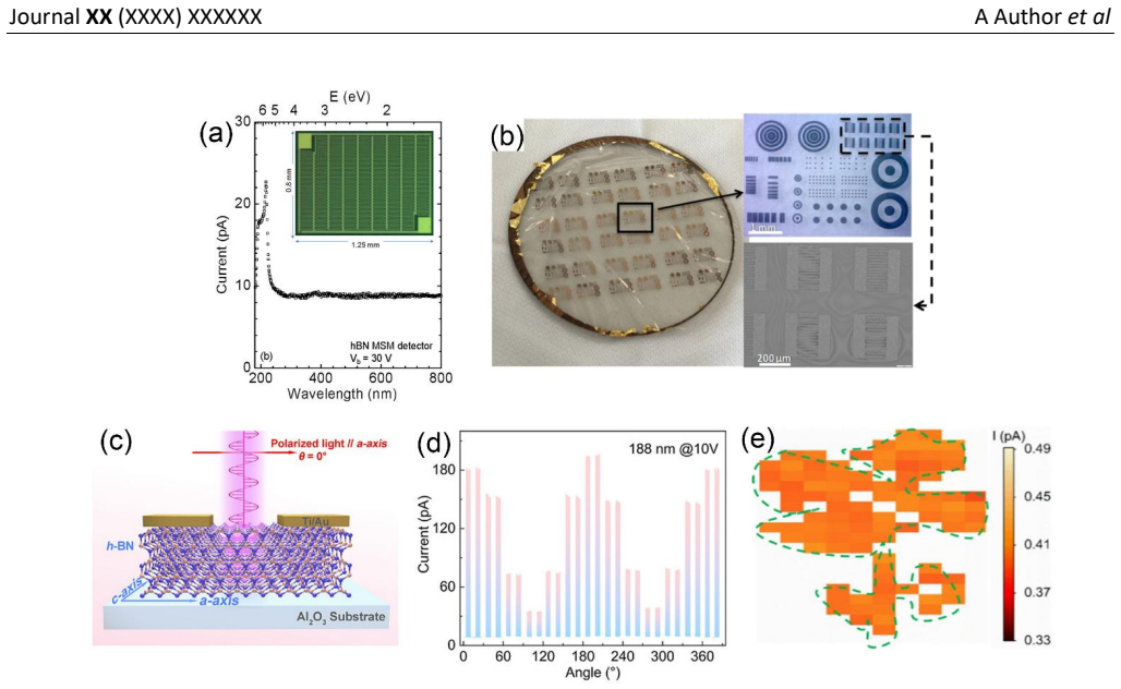
The organizing device is a common set of photodetector figures of merit — spectral responsivity $R$, noise spectral density, noise equivalent power, specific detectivity $D^* = \sqrt{A\,\Delta f}/\mathrm{NEP}$, linear dynamic range, rise/fall time, 3 dB bandwidth and roll-off — defined in Section 2 and used as the benchmark language for all materials. Around that metric framework, each chapter's argument is carried by a material-specific mechanism: Ga2O3's photoconductive gain from hole trapping, AlGaN's composition-tunable bandgap and avalanche gain, BN and diamond's ultra-wide-bandgap absorption and radiation tolerance, MgZnO's bandgap engineering toward 280 nm, perovskite chloride composition for solar-blind absorption, and MEMS strain and piezotronic effects that break the responsivity–dark-current trade-off. The roadmap's comparative claim rests on reading all platforms through the same metric grid.
What would settle it
A concrete test would be an interlaboratory round-robin: take representative Ga2O3, AlGaN, SiC, and diamond photodetectors, measure spectral responsivity, noise spectral density, and $D^*$ under identical bias and illumination conditions, and check whether the relative maturity and bottleneck rankings described in the roadmap survive. A second, simpler check is bibliometric: if a systematic search shows that reported Ga2O3 responsivities above $10^5$ A/W come exclusively from measurements where gain and noise were characterized under different conditions, the roadmap's 'high responsivity, slow response' characterization would need revision.
Extended reading notes
Core claim
The central claim is that UV-C detection is at a technology transition: the combination of emerging UV-C light sources and maturing wide-bandgap semiconductor platforms is creating detector capabilities — spectrally selective, solar-blind response, radiation hardness, fast response, and on-chip integration — that the paper organizes into a coherent landscape. For each material the chapter authors state a status, current challenges, and advances: Ga2O3 offers very high responsivity but seconds-scale response times and no mature p-type doping; AlGaN offers a tunable bandgap and avalanche or single-photon operation but needs better AlN substrates and defect control; diamond and BN offer extreme robustness and solar blindness but limited wafer scale and contact engineering; MgZnO offers Si-compatible, low-cost potential but suffers persistent photoconductivity; perovskite and 2D platforms offer flexibility and low-temperature processing but face degradation and scaling issues; MEMS adds strain-based performance tuning and dual-modality detection. Across applications — metrology, astronomy, communications, environmental monitoring, fire detection, missile warning, gas sensing, and medical diagnostics — the roadmap identifies the detector requirements and the market pull, concluding that no single platform wins everywhere and that the bottlenecks are mostly material-level rather than application-level.
Load-bearing premise
The roadmap's conclusions rest on the assumption that the cited literature is representative and that the chapter authors' qualitative judgments about material maturity and bottlenecks are accurate; the paper does not independently verify the source papers' measurements or claims.
Editorial extensions
If this is right
- If the roadmap's maturity assessment is right, Ga2O3 detectors will first reach deployment in slow-response applications such as exoplanet spectroscopy, environmental monitoring, and gas sensing, where their high responsivity outweighs their seconds-scale temporal response.
- AlGaN, with demonstrated avalanche gains and Geiger-mode operation, is the most plausible route to practical UV-C single-photon detection and UV-C communications receivers.
- Large-area wafers — 6-inch Ga2O3, 100 mm AlN, 3.5-inch diamond — plus the first integrated SiC CMOS image sensor will push UV-C detection from single devices toward arrays and imaging systems.
- Metal halide perovskite and 2D-material detectors, if their degradation and scaling issues are solved, would enable low-cost, flexible, large-area UV-C sensing for wearables and IoT, a market the roadmap identifies as emerging.
- MEMS-based detectors offer a route around the responsivity-speed compromise, and their dual photo-electric and photo-thermal transduction could enable multifunctional UV-C sensors.
Reading between the lines
- My inference, extending the roadmap's own framing: the filter-free solar-blind property is the single feature that could open the largest new market, fire detection in sunlight, but the paper states that no current photodiode achieves the required eight-order-of-magnitude UV-A and UV-B rejection; a testable target for materials development is therefore a photodiode with a spectral rejection ratio
- A quantitative extension the roadmap leaves implicit: a standardized, application-agnostic benchmark that reports $D^*$ measured under the same bias and gain conditions across all platforms would convert the qualitative maturity rankings into a testable leaderboard.
- The roadmap's bottleneck inventory suggests a convergence prediction: whichever platform first combines large-area substrates, low defect density, and a true p-n junction will dominate imaging arrays, because the application chapters repeatedly demand uniform large focal planes rather than single-pixel sensitivity.
- If UV-C LEDs become stable broadband reference sources, the metrology chapter implies that wide-bandgap detectors could shorten SI traceability chains by serving as transfer standards, reducing current UV-C calibration uncertainties toward visible-range levels.
Editorial analysis
A structured set of objections, weighed in public.
Referee Report
Summary. This roadmap reviews the field of UV-C photodetection, assembling multi-author contributions on performance figures of merit, incumbent technologies (Si, SiC, PMTs, CCD/CMOS), emerging material platforms (Ga2O3, AlGaN, BN, diamond, MgZnO, 2D materials, metal halide perovskites, MEMS), and application/industry perspectives (metrology, astronomy, communications, environmental monitoring, fire detection, missile warning, gas sensing, medical diagnostics). The stated aim is to provide a comprehensive and accessible overview for newcomers and a status assessment for experts, with the broader goal of accelerating translation of UV-C photodetectors into practical technologies. The paper is a review/roadmap, not a source of new experimental data.
Significance. If the technical content is corrected, this roadmap would be a valuable reference: it assembles a broad, current, multi-author survey with explicit treatment of device architectures, figures of merit, industry status, and applications, and it provides an extensive set of up-to-date references. The Section 2 tutorial on performance figures of merit is intended to be the common comparative language for the later material chapters, but it currently contains quantitative errors that would mislead newcomers. The breadth of coverage and the expert authorship of individual chapters are strengths; however, the reliability of the roadmap as a benchmark source depends on correcting the technical inaccuracies noted below.
major comments (3)
- [Section 2 (Frequency Response; Figure 1a caption)] The stated roll-off of -10 dB/decade is inconsistent with the given first-order low-pass transfer function R(f) ∝ sqrt(τ)/[1+(2πfτ)^2]^{1/2}. For f >> 1/(2πτ) this expression asymptotes as R ∝ 1/f, which corresponds to -20 dB/decade on a Bode plot. The same incorrect value is repeated in the Figure 1a caption. In addition, the Butterworth sentence states that 'f3dB and the roll-off decrease with increasing n'; the roll-off magnitude actually increases (steepens) with n, and for the given Butterworth form R(f) ∝ sqrt(τ)/[1+(2πfτ)^{2n}]^{1/2}, the -3 dB frequency is independent of n (f3dB = 1/(2πτ)), not decreasing. The caption's '4th order BWF -40 dB/decade' corresponds to n=2, not n=4. Because this section is the tutorial framework for all later material comparisons, these errors need correction.
- [Section 4.4 (Status, first paragraph)] Diamond is described as having a 'direct bandgap energy (~5.5 eV)'. Diamond is a well-established indirect bandgap semiconductor with a bandgap of about 5.47 eV. This factual error affects the discussion of absorption and photodetector physics in the diamond chapter and should be corrected; any statements that rely on direct-gap behavior should be revisited.
- [Section 4.3 (Status, first paragraph)] The text lists 'exceptional dielectric strength (κ~3-4 for h-BN [2] and 1-2 for amorphous phase [3])'. The symbol κ denotes the dielectric constant (relative permittivity), not dielectric strength, which has units of electric field (e.g., V/cm or MV/cm). The cited values appear to be permittivities, so the term 'dielectric strength' is misused. This is a technical inaccuracy in a materials chapter that otherwise provides a useful survey of BN properties.
minor comments (5)
- [Section 2 (Noise Spectral Density)] The general expression for NSD includes a generation-recombination term i_{g-r}, but the explicit square-bracket formula is written as [2q<i_d> + 4k_BT/R_sh + i_{1/f}^2(f)]; the i_{g-r} term is dropped and the 1/f notation appears as a squared quantity. This should be made notationally consistent.
- [Sections 4.3 and 4.6] The bandgap of h-BN is quoted as 6.0–6.4 eV in Section 4.3 but as 5.7 eV in Section 4.6; the two chapters should be cross-consistent, with appropriate references for the value used.
- [Section 4.8 (MEMS, Status)] The thermal conductivity of diamond is quoted as '22 W/mm K'. The correct value is approximately 22 W/cm·K (2200 W/m·K), i.e., 2.2 W/mm·K. The unit error should be fixed.
- [Section 3 (Incumbent technology, reference [6])] Reference [6] (Nakagomi et al.) is cited as an Applied Physics Letters article, but the DOI given (10.1016/j.sna.2015.06.011) corresponds to a Sensors and Actuators A publication; the reference metadata should be verified and corrected.
- [Section 4.1 (reference [7])] The journal name in reference [7] is misspelled as 'Semicontor Science and Technology'; it should be 'Semiconductor Science and Technology'.
Circularity Check
No significant circularity: this is a roadmap/review that aggregates independently published results; the Section 2 roll-off error is a correctness defect, not a circular derivation.
full rationale
This manuscript is an expert roadmap/review rather than a derivation chain. Its central content is a survey of independently published material and device results, with no fitted parameter that is later presented as a prediction and no quantity defined in terms of the conclusion it supports. Section 2 defines standard figures of merit (NSD, responsivity, D*, f3dB, roll-off) using conventional definitions and external references (Jones 1953, 1957, 1949; Fang et al. 2019; Campbell et al. 2002; Tasker et al. 2021), and these definitions are not used to force any later chapter conclusion. The later chapters cite some of the authors' own prior publications for specific device records (e.g., diamond photodetectors in Section 4.4, MgZnO devices in Section 4.5, niobate detectors in Section 4.6), but those are independently published experimental results used as literature entries; they are not load-bearing self-citations that substitute for evidence. The reviewer-identified statement that a first-order low-pass response rolls off at -10 dB/decade is numerically inconsistent with the given transfer function R(f) ∝ 1/f at high frequencies, which gives -20 dB/decade, and the Butterworth sentence about n-dependence is also inverted; however, this is a correctness/technical-editorial defect in the tutorial section, not a circular step, because the figures of merit are not defined in terms of each other or of the roadmap's conclusions. No prediction reduces by construction to an input, no uniqueness claim is imported from the authors' prior work, and no ansatz is smuggled in via citation.
Assumptions & free parameters
assumptions (3)
- domain assumption Reported figures of merit in the cited literature are reliable and measured under the stated conditions.
- domain assumption Standard photodetector noise and frequency response models apply to UV-C materials.
- domain assumption The bandgap values and material properties of the listed semiconductors are correct as cited.
Cite this review
Pith. "Pith review of Roadmap on UV-C photodetectors: materials, applications and industry perspectives." pith.science (2026). https://pith.science/paper/OA5ROC76
@misc{pith2026260807049,
  author       = {Pith},
  title        = {Pith review of: Roadmap on UV-C photodetectors: materials, applications and industry perspectives},
  year         = {2026},
  howpublished = {\url{https://pith.science/paper/OA5ROC76}},
  note         = {Machine review of arXiv:2608.07049}
}
read the original abstract
UV-C photodetectors are poised to play an increasingly important role in future photonic technologies, driven by the rapid emergence of UV-C light sources and new wide bandgap semiconductors. These advances are enabling new levels of spectral selectivity, radiation hardness, sensitivity, and device integration, while opening opportunities across a broad range of applications. This roadmap provides a comprehensive overview of the current landscape of UV-C photodetection, spanning established and emerging material platforms (Ga2O3, AlGaN, BN, diamond, MgZnO, 2-dimensional materials, metal halide perovskites, micro-electromechanical systems), and their applications in metrology, astronomy, communications, environmental monitoring, fire detection, missile warning, gas sensing, and medical diagnostics. By identifying opportunities, bottlenecks, and future directions, this roadmap aims to support both newcomers and established researchers, with the aim of accelerating the translation of UV-C photodetectors into impactful technologies.
Figures


Figures from the paper (14 more)




Reference graph
Works this paper leans on
-
[2]
Zhang Y, Kang L, Wong I H M, Dai W, Li X, Chan R C K, Hsin M K Y and Wong T T W 2022 High-throughput, label-free and slide- free histological imaging by computational microscopy and unsupervised learning Advanced Science 9 e2102358 (doi: 10.1002/advs.202270012)
-
[3]
Ojaghi A, Carrazana G, Caruso C, Abbas A, Myers D R, Lam W A and Robles F E 2020 Label-free hematology analysis using deep- ultraviolet microscopy Proc. Natl. Acad. Sci. U. S. A. 117 14779 (doi: 10.1073/pnas.2001404117)
-
[1]
Kumamoto Y, Taguchi A and Kawata S 2019 Deep-ultraviolet biomolecular imaging and analysis Advanced Optical Materials 7 1801099 (doi: 10.1002/adom.201801099)
-
[4]
Domes C, Domes R, Popp J, Pletz M W and Frosch T 2017 Ultrasensitive detection of antiseptic antibiotics in aqueous media and human urine using deep UV resonance Raman spectroscopy Analitical Chemistry 89 9997 (doi: 10.1021/acs.analchem.7b02422)
-
[5]
Demeersseman N, Saegeman V, Cossey V, Devriese H and Schuermans A 2023 Shedding a light on ultraviolet-C technologies in the hospital environment Journal of Hospital Infection 132 85 (doi: 10.1016/j.jhin.2022.12.009)
-
[6]
Kasaragod D K and Aizawa H 2023 Deep ultraviolet fluorescence microscopy of three-dimensional structures in the mouse brain Scientific Reports 13 8553 (doi: 10.1038/s41598-023-35650-2)
-
[7]
Harz M, Claus R A, Bockmeyer C L, Baum M, Rosch P, Kentouche K, Deigner H P and Popp J 2006 UV-resonance Raman spectroscopic study of human plasma of healthy donors and patients with thrombotic microangiopathy Biopolymers 82 317 (doi: 10.1002/bip.20489)
- [8]
Show all 20 references
-
[9]
Blatchley III E R, Brenner D J, Claus H, Cowan T E, Linden K G, Liu Y, Mao T, Park S-J, Piper P J and Simons R M 2023 Far UV-C radiation: An emerging tool for pandemic control Critical Reviews in Environmental Science and Technology 53 733 (doi: 10.1080/10643389.2022.2084315)
2023
-
[10]
Bergman R S 2021 Germicidal UV sources and systems Photochemistry and Photobiology 97 466 (doi: 10.1111/php.13387)
2021 doi
-
[11]
Chen X H, Ren F F, Gu S L and Ye J D 2019 Review of gallium-oxide-based solar-blind ultraviolet photodetectors Photonics Research 7 381 (doi: 10.1364/PRJ.7.000381)
2019 doi
-
[12]
Cai Q, You H, Guo H, Wang J, Liu B, Xie Z, Chen D, Lu H, Zheng Y and Zhang R 2021 Progress on AlGaN-based solar-blind ultraviolet photodetectors and focal plane arrays Light: Science & Applications 10 94 (doi: 10.1038/s41377-021-00527-4) Journal XX (XXXX) XXXXXX A Author et al 88
2021 doi
-
[13]
Yu H B, Memon M H, Yao M J, Gao Z X, Luo Y M, Kang Y, Zhan Q Q, Chen W, Chen Y P, Liu S, Yang Z Y, Hasan T and Sun H D 2025 A miniaturized cascaded-diode-array spectral imager Nature Photonics 19 1322 (doi: 10.1038/s41566-025-01754-6)
2025 doi
-
[14]
Rivenson Y, Wang H, Wei Z, de Haan K, Zhang Y, Wu Y, Gunaydin H, Zuckerman J E, Chong T, Sisk A E, Westbrook L M, Wallace W D and Ozcan A 2019 Virtual histological staining of unlabelled tissue-autofluorescence images via deep learning Nature Biomedical Engineering 3 466 (doi:...
2019 doi
-
[15]
Bai B, Yang X, Li Y, Zhang Y, Pillar N and Ozcan A 2023 Deep learning-enabled virtual histological staining of biological samples Light: Science & Applications 12 57 (doi: 10.1038/s41377-023-01104-7)
2023 doi
-
[16]
Fereidouni F, Harmany Z T, Tian M, Todd A, Kintner J A, McPherson J D, Borowsky A D, Bishop J, Lechpammer M, Demos S G and Levenson R 2017 Microscopy with ultraviolet surface excitation for rapid slide-free histology Nature Biomedical Engineering 1 957 (doi: 10.1038/s41551-017-0165-y)
2017 doi
-
[17]
Kneissl M, Seong T-Y, Han J and Amano H 2019 The emergence and prospects of deep-ultraviolet light-emitting diode technologies Nature Photonics 13 233 (doi: 10.1038/s41566-019-0359-9)
2019 doi
-
[18]
Sliney D H and Stuck B E 2021 A need to revise human exposure limits for ultraviolet UV-C radiation Photochemistry and Photobiology 97 485 (doi: 10.1111/php.13402)
2021 doi
-
[19]
Moseley H, Allan D, Amatiello H, Coleman A, du Peloux Menage H, Edwards C, Exton L S, Ferguson J, Garibaldinos T, Martin C and Mohd Mustapa M F 2015 Guidelines on the measurement of ultraviolet radiation levels in ultraviolet phototherapy British journal of Dermatology 173 333...
2015 doi
-
[20]
Concluding remarks Fabien Massabuau1 1 Department of Physics, SUPA, University of Strathclyde, Glasgow, United Kingdom E-mail: f.massabuau@strath.ac.uk UV-C photodetectors are entering an important phase of development, driven by rapid advances in wide bandgap semiconductors, ...
Reviewed August 10, 2026 · model on record in the stance chip above.
Discussion (0). Continue with ORCID to comment.