REVIEW 2 major objections 5 minor 10 references
Study of GeSn Selective Area Growth with Demonstration of SWIR Light Detection
T0 review · 2 major / 5 minor · reviewed 2026-08-01 · deepseek-v4-flash
Pith's one-line read GeSn selectively grown on patterned silicon detects light out to 2 µm.
desk verdict A credible first demonstration of GeSn SAG photoconductors with a 2 µm cutoff, held back by ensemble-averaged composition data and missing uncertainties. read the letter →
The pith
A machine-rendered reading of the paper's core claim, the machinery that carries it, and where it could break.
The reading
What carries the argument
The central mechanism is the loading effect in selective area growth. With a fixed flux of GeH4 and SnCl4, the effective growth rate in an open window increases as the window size or pattern fill factor decreases, because the surrounding mask area contributes precursors to the window. This mechanism carries the explanation for the paper's central observations: faster overgrowth in small windows, weakened or absent Sn incorporation at sub-10 µm sizes, and Sn droplet formation in high-Sn recipes.
What would settle it
Measure the composition of one of the actual 100 µm square device islands (e.g., with focused micro-XRD or EDX/TEM cross-section) and compare it to the 7.1% Sn value from the wafer-averaged RSM. If that island's composition is materially different, the 2 µm cutoff attribution and the responsivity values would need re-evaluation.
Extended reading notes
Core claim
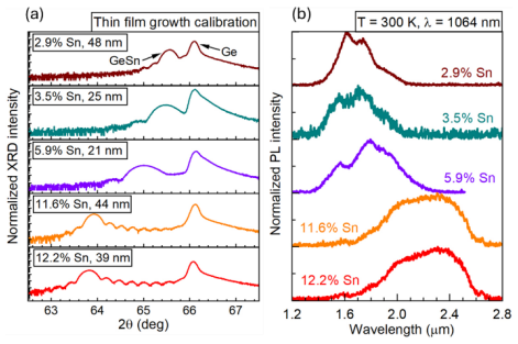
On SiO2-patterned Si substrates with windows from 2 µm to 100 µm and shapes including circle, square, octagon, and rectangle, GeSn selective area growth yields good optical quality with Sn contents from 3.2% to 8.7%. Photoluminescence red-shifts with Sn content, from 1.6 µm for Ge SAG to 2.1 µm for the 8.7% Sn sample. Photoconductors made on 100 µm square islands show responsivity up to 0.9 A/W at 1.55 µm for the 4.2% Sn sample and 0.2 A/W at 2 µm for the 7.1% Sn sample, with detection cutoffs at 1.89 µm and 2 µm respectively. The paper also reveals a loading effect in GeSn SAG: growth rate increases as window size or fill factor shrinks, which degrades crystal quality in high-Sn recipes and
Load-bearing premise
The tin contents quoted for the SAG samples come from X-ray reciprocal-space maps that average over many windows of different sizes, and are assumed to match the specific 100 µm square islands from which the photoconductor data are taken.
Editorial extensions
If this is right
- GeSn SAG can produce composition-tunable infrared emitters and detectors in predefined locations, offering a path to integrating GeSn with Si waveguides or focal-plane arrays.
- Detection cutoff wavelength scales with Sn content in SAG islands, demonstrated from 1.89 µm at 4.2% Sn to 2 µm at 7.1% Sn, with PL reaching 2.1 µm at 8.7% Sn.
- The loading effect means thin-film calibration recipes do not transfer directly to SAG; small windows require recipe adjustment to preserve Sn incorporation.
- High-Sn SAG is prone to Sn segregation and droplet formation unless the window shape provides enough fill factor, with rectangle windows the most robust in this study.
Reading between the lines
- If the single-island composition were confirmed directly, the 2 µm cutoff would make GeSn SAG photoconductors candidates for low-cost extended-SWIR sensing on a CMOS-compatible platform.
- The loading effect likely scales with adatom diffusion length, so at nanometer window sizes the Sn-suppression threshold could shift with growth pressure and precursor choice; this suggests a testable recipe map.
- The PL being dominated by direct-gap emission even in Ge SAG hints that small islands geometrically suppress the indirect emission, which may exaggerate the apparent 'directness' of low-Sn SAG material; comparing absorption or time-resolved PL across window sizes would separate geometry from band-structure effects.
Editorial analysis
A structured set of objections, weighed in public.
Referee Report
Summary. This paper reports selective area growth (SAG) of GeSn in SiO2 windows on Si by RPCVD, for window sizes from 2 to 100 um and circle, octagon, square, and rectangle shapes. The authors claim successful Sn incorporation from 3.2% to 8.7%, tunable photoluminescence from roughly 1.6 to 2.1 um, and a GeSn SAG photoconductor on a 100 um square island with detection cutoff up to 2 um. They also report a loading effect that increases growth rate as window size or fill factor decreases, leading to reduced Sn incorporation at small window sizes and Sn segregation in high-Sn recipes. Composition is extracted from (224) RSM over a ~5 mm2 beam that averages many windows; the evidence also includes PL, SEM-EDX, micro-Raman, TEM, temperature-dependent I-V, and FTIR spectral response.
Significance. If the composition attribution is correct, this is a notable advance: it demonstrates a working micro-scale GeSn SAG photoconductor, extends GeSn SAG to Sn contents up to 8.7%, and provides useful empirical data on the loading effect. The paper is strengthened by the use of multiple independent characterization techniques, temperature-dependent device measurements, and explicit disclosure of the discrepancy between direct laser and FTIR responsivity. I find no circularity: the thin-film calibration and prior GeSn detector results are used as independent inputs. However, the paper's own micro-Raman data show a strong dependence of Sn incorporation on window size, and the RSM-derived compositions are ensemble averages; this gap must be closed before the quantitative composition range and the 7.1% Sn attribution for the 2 um cutoff can be taken as established.
major comments (2)
- [XRD and Table 1; Figs. 3, 8] The Sn contents in Table 1 (3.2-8.7%) come from (224) RSM with a ~5 mm2 beam, an average over many windows, as the paper itself states. For sample 4 the RSM was on a circle window (Fig. 3 caption), while the device is on a single 100 um square island. Micro-Raman (Fig. 8c,f) shows the Ge-Sn mode disappears in 2 um square windows and is weaker at 10 um, so composition is strongly size-dependent. No measurement ties the RSM average to the device island, and the RSM analysis does not state how strain relaxation is deconvolved from composition. Provide a direct composition/strain measurement of the 100 um square island (micro-XRD or EDX) or a quantitative uncertainty analysis over window sizes/shapes; otherwise the 2 um cutoff attribution to 7.1% Sn and the 3.2-8.7% range are not fully supported.
- [Photoconductor responsivity and D*; Figs. 5, 6; Eq. (1)] The quantitative device claims (responsivity up to 0.9 A/W, D* comparable to PbSe) rest on an area normalization that is not fully specified: the caption says the ratio of exposed device area to the 320 um laser beam is used, but the exposed/active area is not defined, and no uncertainties or repeat measurements are given. In addition, the FTIR spectra are described as normalized, so it is unclear how the absolute D* spectra in Fig. 6e are obtained from them. Please define the area, state how FTIR spectra were scaled, and add error bars or at least a sensitivity analysis for the area factor.
minor comments (5)
- [Fig. 3g and text] The text uses 6.7% as the boundary below which shape effects are negligible, but sample 3 is 6.7%; please clarify whether sample 3 belongs to the low-Sn group and justify the threshold.
- [Fig. 2 and Loading effect discussion] Please define window size for rectangles (width or length?) and the fill factor used in the loading-effect analysis; these terms are currently used qualitatively.
- [Fig. 6e] The comparison curves for commercial detectors and PbSe are not cited; please add references and specify the operating temperatures and bias conditions.
- [Abstract and Conclusion] The phrase 'good optical quality' is stronger than the evidence presented; PL observation demonstrates radiative quality but not structural quality. Please soften or add defect-density measurements.
- [Methods, FTIR calibration] The FTIR conversion uses an InGaAs detector with cutoff 2.6 um; since sample 4's cutoff is at 2 um, please state whether the calibration is valid to 2.6 um and describe how the noise floor near cutoff is treated.
Circularity Check
No circularity: SAG composition, PL tuning, and photoconductor cutoff are direct measurements; self-citations are calibration/comparison, not load-bearing.
full rationale
All three central claims—GeSn SAG composition 3.2–8.7% Sn, tunable PL, and photoconductor cutoff ≈2 µm—rest on measured quantities (XRD/RSM, PL spectra, FTIR responsivity) rather than on a derivation from an assumed model. The growth recipe was calibrated using thin-film samples (Fig. 1, refs 19–21), but the SAG Sn contents were then independently extracted from (224) RSM data (Fig. 3, Table 1); the RSM extraction is not defined in terms of the device cutoff or the PL peak, so there is no self-definitional loop. The statement that “SAG experimental Sn content closely followed the nominal target” is a consistency check between two independently measured/defined quantities, not a prediction of one from the other. Self-citations (refs 8, 18–22) are used for calibration precedent, earlier unsuccessful SAG context, and performance comparison; none is invoked as a uniqueness theorem or ansatz that forces the reported result. The manuscript itself notes that XRD and PL signals are averaged over many windows of different sizes (Figs. 3–4), which is a real limitation on attributing the average 7.1% Sn to the specific 100 µm square device island; however, that is a sampling/metrology validity concern, not circularity, because the composition value is not constructed from the device response. I find no load-bearing step that reduces a prediction to a fitted input or to a self-citation chain; the nonzero score reflects only the presence of minor non-load-bearing self-citations for calibration.
Assumptions & free parameters
free parameters (2)
- Responsivity area normalization ratio =
not explicitly reported; ratio of exposed device area to 320-µm-diameter laser beam used
- XRD composition conversion (lattice constant vs Sn fraction) =
standard relation via refs 19–21
assumptions (7)
- ad hoc to paper Thin-film growth calibration transfers directly to SAG growth rate
- domain assumption XRD average over many SAG windows represents bulk SAG composition
- domain assumption TEM cross-sections are representative of SAG islands
- domain assumption HCl maintains selectivity without materially changing Sn uptake
- domain assumption Raman Ge(F2g) shift can be interpreted as composition/strain via published calibrations
- domain assumption PL direct-gap dominance from SAG islands reflects small absorption volume
- domain assumption Detection cutoff at 50% FTIR relative intensity is a meaningful device metric
Cite this review
Pith. "Pith review of Study of GeSn Selective Area Growth with Demonstration of SWIR Light Detection." pith.science (2026). https://pith.science/paper/2JGVBGOA
@misc{pith2026260716497,
  author       = {Pith},
  title        = {Pith review of: Study of GeSn Selective Area Growth with Demonstration of SWIR Light Detection},
  year         = {2026},
  howpublished = {\url{https://pith.science/paper/2JGVBGOA}},
  note         = {Machine review of arXiv:2607.16497}
}
read the original abstract
As germanium-tin (GeSn) epitaxial growth quality continuously improves, the search for an efficient integration strategy of GeSn optoelectronics devices into complementary metal-oxide-semiconductor (CMOS) manufacturing line also accelerates. Selective area growth (SAG) on patterned substrate emerges as a promising approach for this quest, with locally controlled growth of GeSn laser/detector suitable for either co-integration with silicon-based waveguide structure or stand-alone module like focal plane array. In this work, we report successful GeSn SAG with Sn content ranging from 3.2% to 8.7% of good optical quality, with demonstration of tunable GeSn SAG photoluminescence and GeSn SAG photoconductor device, the latter with detection cutoff wavelength up to 2 um. In addition, we present a comprehensive study of GeSn SAG condition at different window sizes, from 2 um to 100 um, and shapes: circle, square, octagon, and rectangle. Presence of loading effect is revealed, where GeSn growth rate increases as pattern fill factor and window size shrink. It introduces a different growth condition compared to thin film growth, which can weaken or inhibit Sn incorporation at very small window size and induce Sn segregation in high Sn content SAG growth.
Figures
Reference graph
Works this paper leans on
-
[1]
Lasing in Direct-Bandgap GeSn Alloy Grown on Si
(1) Wirths, S.; Geiger, R.; von den Driesch, N.; Mussler, G.; Stoica, T.; Mantl, S.; Ikonic, Z.; Luysberg, M.; Chiussi, S.; Hartmann, J.-M.; Sigg, H.; Faist, J.; Buca, D.; Grutzmacher, D. Lasing in Direct-Bandgap GeSn Alloy Grown on Si. Nat. Photonics 2015, 9,
2015
-
[88]
M.; Frauenrath, M.; Casiez, L.; Chelnokov, A.; Reboud, V.; Hartmann, J.-M.; El-Kurdi, M.; Pauc, N.; Calvo, V
(2) Chretien, J.; Thai, Q. M.; Frauenrath, M.; Casiez, L.; Chelnokov, A.; Reboud, V.; Hartmann, J.-M.; El-Kurdi, M.; Pauc, N.; Calvo, V. Room Temperature Optically Pumped GeSn Microdisk Lasers. Appl. Phys. Lett. 2022, 120, 051107. (3) Bjelajac, A.; Gromovyi, M.; Sakat, E.; Wang, B.; Patriarche, G.; Pauc, N.; Calvo, V.; Boucaud, P.; Boeuf, F.; Chelnokov, A...
2022
-
[115]
I.; Patra, S
(12) De Koninck, Y.; Caer, C.; Yudistira, D.; Baryshnikova, M.; Sar, H.; Hsieh, P.-Y.; Özdemir, C. I.; Patra, S. K.; Kuznetsova, N.; Colucci, D.; Milenin, A.; Yimam, A. A.; Morthier, G.; Van Thourhout, D.; Verheyen, P.; Pantouvaki, M.; Kunert, B.; Van Campenhout, J. GaAs Nano-Ridge Laser Diodes Fully Fabricated in a 300-Mm CMOS Pilot Line. Nature 2025, 63...
2025
-
[207]
The Effect of Ge Precursor on the Heteroepitaxy of Ge1−xSnx Epilayers on a Si (001) Substrate
(41) Jahandar, P.; Weisshaupt, D.; Colston, G.; Allred, P.; Schulze, J.; Myronov, M. The Effect of Ge Precursor on the Heteroepitaxy of Ge1−xSnx Epilayers on a Si (001) Substrate. Semicond. Sci. Technol. 2018, 33 (3), 034003. 26 (42) Hartmann, J. M.; Marion, T. An Assessment of Germane and Tin Tetrachloride for GeSn Epitaxy. J. Cryst. Growth 2025, 667, 12...
2018
-
[225]
L.; Hersee, S.; Han, S
(44) Li, Q.; Krauss, J. L.; Hersee, S.; Han, S. M. Probing Interactions of Ge with Chemical and Thermal SiO2 to Understand Selective Growth of Ge on Si during Molecular Beam Epitaxy. The Journal of Physical Chemistry C 2007, 111 (2), 779–786. (45) Wirths, S.; Buca, D.; Tiedemann, A. T.; Holländer, B.; Bernardy, P.; Stoica, T.; Grützmacher, D.; Mantl, S. E...
2007
-
[2009]
F.; Schmid, H.; Sousa, M.; Gooth, J.; Riel, H.; Moselund, K
(15) Wirths, S.; Mayer, B. F.; Schmid, H.; Sousa, M.; Gooth, J.; Riel, H.; Moselund, K. E. Room-Temperature Lasing from Monolithically Integrated GaAs Microdisks on Silicon. ACS Nano 2018, 12 (3), 2169–2175. (16) Staudinger, P.; Moselund, K. E.; Schmid, H. Exploring the Size Limitations of Wurtzite III–V Film Growth. Nano Lett. 2020, 20 (1), 686–693. 24 (...
2018
-
[2022]
A.; Ong, S
(27) Tran, R.; Xu, Z.; Radhakrishnan, B.; Winston, D.; Sun, W.; Persson, K. A.; Ong, S. P. Surface Energies of Elemental Crystals. Sci. Data 2016, 3 (1), 160080. (28) Aubin, J.; Hartmann, J.-M.; Gassenq, A.; Rouviere, J. L.; Robin, E.; Delaye, V.; Cooper, D.; Mollard, N.; Reboud, V.; Calvo, V. Growth and Structural Properties of Step-Graded, High Sn Conte...
2016
-
[2026]
D.; Orzali, T.; Merckling, C.; Brammertz, G.; Ong, P.; Winderickx, G.; Hellings, G.; Eneman, G.; Caymax, M.; Meuris, M.; Horiguchi, N.; Thean, A
(11) Waldron, N.; Wang, G.; Nguyen, N. D.; Orzali, T.; Merckling, C.; Brammertz, G.; Ong, P.; Winderickx, G.; Hellings, G.; Eneman, G.; Caymax, M.; Meuris, M.; Horiguchi, N.; Thean, A. Integration of InGaAs Channel N-MOS Devices on 200mm Si Wafers Using the Aspect-Ratio-Trapping Technique. ECS Trans. 2012, 45 (4),
2012
Show all 10 references
-
[3954]
Room Temperature Lasing in GeSn Microdisks Enabled by Strain Engineering
(4) Buca, D.; Bjelajac, A.; Spirito, D.; Concepción, O.; Gromovyi, M.; Sakat, E.; Lafosse, X.; Ferlazzo, L.; von den Driesch, N.; Ikonic, Z.; Grützmacher, D.; Capellini, G.; El Kurdi, M. Room Temperature Lasing in GeSn Microdisks Enabled by Strain Engineering. Adv. Opt. Mater....
2022
-
[5640]
Enhanced Sn Incorporation in GeSn Epitaxial Semiconductors via Strain Relaxation
(20) Assali, S.; Nicolas, J.; Moutanabbir, O. Enhanced Sn Incorporation in GeSn Epitaxial Semiconductors via Strain Relaxation. J. Appl. Phys. 2019, 125 (2), 025304. (21) Stanchu, H. V; Kuchuk, A. V; Mazur, Y. I.; Margetis, J.; Tolle, J.; Yu, S.-Q.; Salamo, G. J. Strain Suppre...
2019
Reviewed August 1, 2026 · model on record in the stance chip above.
Discussion (0). Sign in to comment.