REVIEW 3 major objections 7 minor 16 references
Radiation effects on surface and bulk properties of ATLAS18 silicon sensors under low- and high-dose gamma irradiation and annealing
T0 review · 3 major / 7 minor · reviewed 2026-08-02 · deepseek-v4-flash
Pith's one-line read Low-dose gamma irradiation of ATLAS18 strip sensors changes the surface but leaves the silicon bulk undamaged, and high-temperature annealing restores leakage currents.
desk verdict Solid low-dose gamma damage study for ATLAS18 strip sensors, but the headline claim overreaches: V_FD unchanged is only shown up to 15 krad, not the full 0.5–100 krad range. read the letter →
The pith
A machine-rendered reading of the paper's core claim, the machinery that carries it, and where it could break.
The reading
What carries the argument
The load-bearing mechanism is the decomposition I_tot = I_bulk + I_surf, combined with the full depletion voltage extracted from capacitance-voltage curves. In unsegmented diodes, a contactable guard ring measures the two currents separately; in miniature strip sensors, the bulk current is inferred as 104 times the per-strip current obtained from the voltage drop across a bias resistor, with the surface current as the remainder. An Arrhenius-type annealing law (activation energy around 0.06-0.11 eV for the low-dose annealing process) is used to compare the thermal stability of surface and bulk components.
What would settle it
Measure the individual leakage current of every strip (or a large random sample) on a mini irradiated to 100 krad and compare the sum with 104 times a single strip's current; a ratio significantly different from 104 would break the bulk/surface split. Alternatively, if full depletion voltage shifts after low-dose irradiation in a more sensitive test, the 'no bulk damage' claim would be contradicted.
Extended reading notes
Core claim
At low gamma doses relevant to the early ITk phase, the sensor's depletion voltage is unchanged by irradiation and annealing, and the observed leakage-current increase is dominated by the surface current component. The paper reaches this by splitting total current into bulk and surface parts — directly in diodes with a contactable guard ring, and in strip sensors by measuring one strip's current through the bias resistor and multiplying by the 104 strips. At ultra-high gamma doses (hundreds of Mrad), the same devices show genuine bulk damage: depletion voltage drops from about -275 V to about -20 V, and the electric field redistributes into a double-junction structure, consistent with trappe
Load-bearing premise
The mini-sensor bulk current is computed as 104 times the current in one strip, which holds only if all strips carry the same current and inter-strip coupling is negligible; the paper checks bias-resistance uniformity on just six random strips and three edge strips.
Editorial extensions
If this is right
- During the early ITk period, gamma-induced leakage current in ATLAS18 sensors will come almost entirely from surface states, so it will saturate rather than keep growing with dose.
- Full depletion voltage will remain stable at low gamma doses, so the sensors' bias settings and charge-collection behaviour should not need compensation for bulk damage.
- High-temperature annealing above about 250-300 C can restore leakage currents to near pre-irradiation values after low doses, and largely restore the depletion voltage after ultra-high doses.
- At hundreds of Mrad, pure gamma irradiation can produce bulk damage with space-charge redistribution; this damage is not permanent and responds to high-temperature annealing.
- The temperature dependence of the leakage current follows the standard activation energy of about 1.21 eV, so existing scaling formulas can be used to extrapolate measurements to different operating temperatures.
Reading between the lines
- Inference: if the ~2 Mrad surface-current saturation holds on full-size sensors, then integrated ionizing dose in the early tracker could rise well above the qualification limit before leakage becomes a problem, since bulk damage from gamma alone is negligible.
- Inference: the unchanged depletion voltage at low doses implies charge-collection efficiency and spatial resolution should stay unchanged; a direct CCE measurement on irradiated minis, not reported here, would test this cleanly.
- Inference: the per-strip bias-resistor method could be extended to map strip-to-strip current uniformity on full-size sensors; if deviations appear, the 104x multiplication used to estimate bulk current would need revising.
Editorial analysis
A structured set of objections, weighed in public.
Referee Report
Summary. The paper reports a combined gamma-irradiation study of ATLAS18 miniature strip sensors (minis) and MD8 diodes, covering low TIDs of 0.5–100 krad relevant to early ITk operation, together with supplementary measurements at higher doses (up to 3 Mrad for minis, 24 Mrad for diodes, and 630 Mrad in prior high-dose studies). The authors measure total, bulk, and surface leakage currents, extract full depletion voltage from CV measurements, perform isochronal and isothermal annealing, and use TCT on high-dose samples. The central claim, stated in Section 4, is that for low TID levels relevant to ITk operation the full depletion voltage V_FD remains unchanged after irradiation and annealing, indicating that the observed effects are predominantly surface-related and do not produce measurable bulk damage. The paper also reports surface-current saturation around 1–2 Mrad, activation energies for annealing and for leakage-current temperature dependence, and high-temperature annealing recovery for both low- and high-dose samples.
Significance. If the central claim holds, it is reassuring for early HL-LHC ITk strip operation: leakage increases would originate mostly from surface states and be recoverable by high-temperature annealing, while bulk damage would be negligible. The paper's strengths include the combination of segmented and unsegmented devices, a broad TID range from 0.5 krad to several hundred Mrad, and the TCT confirmation of bulk recovery after 300°C annealing of high-dose diodes. However, the load-bearing null result on V_FD is not established over the full claimed low-dose range, and the mini bulk-current decomposition is not fully validated. With additional measurements or a suitably restricted claim, the paper would be a valuable experimental contribution to the ITk radiation-damage literature.
major comments (3)
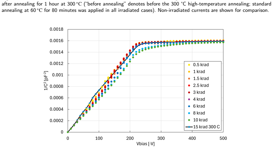
- [Section 4, Fig. 9] The central claim that V_FD remains unchanged for low TID levels relevant to ITk operation is only supported by data up to 15 krad. Section 2 defines the relevant low-dose range as 0.5–100 krad, and IV data are shown up to 100 krad in Fig. 5, but the CV measurements of minis in Fig. 9 cover only TIDs up to 15 krad. No V_FD measurements are presented at 25, 50, or 100 krad. The conclusion in Section 4 therefore extrapolates the null result beyond the measured range. This is load-bearing: the claim that early ITk operation is free of bulk effects depends on this null result. The authors should either extend the CV measurements to the full 0.5–100 krad range or explicitly restrict the claim to the measured dose range.
- [Section 3.2, Fig. 9] The null result for V_FD has no stated uncertainty or sensitivity. The paper does not report the number of samples per dose, the scatter of the CV curves, or the precision of the V_FD extraction. Without a quantitative bound on how much V_FD could change between 15 and 100 krad, the statement that irradiation 'does not induce measurable bulk damage' is not falsifiable. Please provide at least the sample count and an estimate of the V_FD measurement uncertainty, and ideally an upper limit on any possible V_FD change derived from the CV method's resolution.
- [Section 3.1, Fig. 5] The mini bulk-current extraction assumes I_bulk = 104 × I_strip, with I_strip inferred from the voltage drop across the bias resistor. The supporting evidence is the uniformity of the average bias resistance measured on six randomly selected strips and three edge strips (R_bias = (1.584 ± 0.002) MΩ). However, equal bias resistances do not rule out strip-to-strip variations in generation current or interstrip coupling, both of which would directly bias the extraction. Moreover, Fig. 5 shows that the extracted mini bulk current decreases at the upper end of the low-dose range, and the paper itself states that 'the origin of the bulk current decrease at the upper end of the investigated low TID range requires further study.' This unexplained behavior indicates that the bulk/surface decomposition is not yet robust. Please provide a sensitivity analysis of the extraction, or report interstrip
minor comments (7)
- [Throughout] The figures generally lack error bars and sample counts. This is particularly important for Fig. 4 and Fig. 5, where the claim that bulk current remains 'significantly smaller' is made without any measure of reproducibility. Please add error bars or state the number of samples and the run-to-run variability.
- [Section 3.2, Eq. (1)] The Arrhenius-type relation in Eq. (1) uses T_ref as a free parameter, but the fitting procedure and the uncertainties on E and T_ref are not reported. Please clarify how T_ref is determined and provide uncertainties for the values in Table 1.
- [Section 3.4, Table 2] The activation energies for total, bulk, and surface currents are reported to three significant digits, but no uncertainties are given. Given that the text compares these values to the Chilingarov result (1.209 ± 0.007) eV, please provide uncertainties from the fits.
- [Conclusion] There is a typo: 'behaior' should be 'behavior'.
- [References] Reference [12] is cited as 'This Issue' with no further information. Please provide a complete reference or a DOI.
- [Abstract / Section 2] The abstract says 'measurements extending up to a few Mrad,' while the paper reports minis up to 3 Mrad and diodes up to 24 Mrad. Please be consistent, e.g., 'a few Mrad for minis and up to 24 Mrad for diodes.'
- [Fig. 11 and Fig. 12] The TCT-derived V_FD is quoted as '-250 to -300 V' in the text and as '-260 V' from the CCE saturation, but no systematic uncertainty is given. Please state the estimated uncertainty from the pulse-shape and CCE methods.
Circularity Check
No circularity found: central claim rests on direct CV/V_FD and IV measurements, not on fitted inputs or self-citations.
full rationale
The paper is an experimental characterization, not a derivation. The headline conclusion that low TID leaves V_FD unchanged is a measurement result from Fig. 9, and the conclusion that effects are surface-related is supported by the measured dominance of the surface-current component and by the unchanged depletion voltage; neither is obtained by feeding a fitted parameter back into the claim. The Arrhenius forms in Eqs. (1)-(2) are descriptive fits used to report activation energies; the extracted E values are not then used to predict V_FD or the dose dependence, so no fitted input is called a prediction. The mini-sensor bulk current is estimated as I_bulk = 104 × I_strip using the measured bias-resistor voltage drop, which is an experimental procedure with stated uniformity checks; the paper itself notes that this 'bulk' current also contains inter-strip surface components, so the limitation is disclosed rather than hidden by construction. References [5]-[7] are comparisons to the authors' prior work and are not the load-bearing support for the new V_FD result, which is shown in this paper's own CV data. The gap between the 15 krad CV measurements and the 0.5-100 krad range stated as 'relevant' is an extrapolation/sensitivity concern, not a circularity. Therefore no circular step can be quoted, and the appropriate score is 0.
Assumptions & free parameters
free parameters (4)
- Activation energy E_A for leakage current temperature dependence =
1.23, 1.21, 1.20, 1.19, 1.18, 1.16 eV depending on bias (Table 2)
- Pre-exponential factor A in Eq. (2) =
not reported
- Annealing activation energy E in Eq. (1) =
0.064, 0.041, 0.065, 0.113 eV (Table 1)
- Reference temperature T_ref in Eq. (1) =
94.56–104.58 °C
assumptions (5)
- domain assumption 60Co gamma irradiation produces displacement damage only through Compton electrons up to ~1 MeV, creating point defects rather than cluster defects.
- domain assumption The current measured at the guard ring of MD8 diodes represents surface/edge current, while the diode pad current represents true bulk current.
- domain assumption For mini sensors, all 104 strips have identical bias resistance and identical voltage drop, so I_bulk = n × I_strip.
- domain assumption The standard Shockley–Read–Hall generation model and Chilingarov's temperature dependence I(T) = A T^2 exp(-E_A/2kT) describe the bulk and surface leakage currents.
- domain assumption The charge particle equilibrium box ensures uniform energy deposition, so dose values are accurate within the quoted 5% uncertainty.
Cite this review
Pith. "Pith review of Radiation effects on surface and bulk properties of ATLAS18 silicon sensors under low- and high-dose gamma irradiation and annealing." pith.science (2026). https://pith.science/paper/6XMM2N2I
@misc{pith2026260713932,
  author       = {Pith},
  title        = {Pith review of: Radiation effects on surface and bulk properties of ATLAS18 silicon sensors under low- and high-dose gamma irradiation and annealing},
  year         = {2026},
  howpublished = {\url{https://pith.science/paper/6XMM2N2I}},
  note         = {Machine review of arXiv:2607.13932}
}
abstract
Silicon strip detectors for the ATLAS Inner Tracker (ITk) at the HL-LHC must withstand harsh radiation conditions, including fluences of up to 1.6E15 1 MeV n$_{eq}$/cm$^{2}$ and total ionizing doses (TID) of up to 66 Mrad. These requirements are met using radiation-hard n+-in-p technology implemented in the ATLAS18 silicon strip sensors currently under production. This work presents a combined study of gamma-irradiation effects in ATLAS18 silicon sensors, including both segmented miniature strip sensors (minis) and unsegmented MD8 diodes fabricated on ATLAS18 production wafers. The samples were irradiated with a $^{60}$Co gamma source to multiple low TIDs between 0.5 and 100 krad, corresponding to the dose range relevant for the early operational phase of the ITk tracker. Additional measurements extending up to a few Mrad were performed to investigate the saturation of surface related damage effects. Post-irradiation characterization included measurements of total, bulk, and surface leakage currents, as well as capacitance-voltage measurements used to extract the full depletion voltage. The thermal stability of radiation-induced defects was studied using isochronal annealing between 80{\deg}C and 300{\deg}C and isothermal annealing at 60{\deg}C and 160{\deg}C. In addition, complementary studies of MD8 diodes irradiated to ultra-high doses of several hundred Mrad, well beyond the ATLAS ITk requirements, are included to investigate possible bulk-related effects induced by pure gamma irradiation and their annealing behavior. The combined analysis of low- and ultra-high-dose irradiation provides a comprehensive picture of surface- and bulk-related gamma-induced effects in ATLAS18 silicon sensors and their thermal evolution.
Figures


Figures from the paper (10 more)




Reference graph
Works this paper leans on
-
[6]
M.Mikestikovaetal.,Studyofgamma-radiation-induceddisplacementdamagein𝑛 +-in-𝑝silicondiodes,Nucl.Instrum.Meth.A1064(2024) 169432,https://doi.org/10.1016/j.nima.2024.169432
arXiv 2024
-
[7]
Mikestikova et al., Low-dose gamma irradiation study of ATLAS ITk MD8 diodes, JINST20(2025) C08012,https://doi.org/10
M. Mikestikova et al., Low-dose gamma irradiation study of ATLAS ITk MD8 diodes, JINST20(2025) C08012,https://doi.org/10. 1088/1748-0221/20/08/C08012
2025
-
[1]
S.Yoshidaetal.,Radiationhardeningofsiliconstripdetectors,Nucl.Instrum.Meth.A514(2003)38-43,https://doi.org/10.1016/j. nima.2003.08.081
doi:10.1016/j 2003
-
[2]
ATLASCollaboration,TechnicalDesignReportfortheATLASInnerTrackerStripDetector,CERN-LHCC-2017-005,CERN,Geneva(2017)
2017
-
[3]
ATLAS Collaboration, The ATLAS Experiment at the CERN Large Hadron Collider, JINST3(2008) S08003
2008
-
[4]
ATLAS Collaboration, ATLAS Public Results,https://twiki.cern.ch/twiki/bin/view/AtlasPublic/ RadiationSimulationPublicResults#Phase_II_Upgrade_Mar_2018_AN1, accessed 18 May 2026
2026
-
[5]
I. Zatocilova et al., Study of bulk damage of high dose gamma irradiated p-type silicon diodes with various resistivities, JINST19(2024) C02039https://doi.org/10.1088/1748-0221/19/02/C02039
-
[8]
Y. Unno et al., Specifications and pre-production of𝑛+-in-𝑝large-format strip sensors fabricated in 6-inch silicon wafers, ATLAS18, for the Inner Tracker of the ATLAS detector for the High-Luminosity Large Hadron Collider, JINST18(2023) T03008,https://iopscience. iop.org/article/10.1088/1748-0221/18/03/T03008/pdf
Show all 16 references
-
[9]
Unno et al., ATLAS17LS – A large-format prototype silicon strip sensor for long-strip barrel section of ATLAS ITk strip detector, Nucl
Y. Unno et al., ATLAS17LS – A large-format prototype silicon strip sensor for long-strip barrel section of ATLAS ITk strip detector, Nucl. Instrum. Methods Phys. Res. A989(2021) 164928,https://doi.org/10.1016/j.nima.2020.164928
2021
-
[10]
UJP PRAHA a.s.,https://ujp.cz/en/
-
[11]
22900 (2003)
European Space Agency, Total Dose Steady-State Irradiation Test Method, ESCC Basic Specification No. 22900 (2003)
2003
-
[12]
A **This Issue** (2026),
P.Lietal.,Investigationofthecurrent-generationmechanismsintheedgeregionofplanarsiliconsensors,Nucl.Instrum.MethodsPhys.Res. A **This Issue** (2026),
2026
-
[13]
Hirata, M
M. Hirata, M. Hirata, H. Saito; Recombination Centers in Gamma-Irradiated Silicon. J. Appl. Phys. 15 March 1966; 37 (4): 1867–1872, https://doi.org/10.1063/1.1708616
1966 doi
-
[14]
Liao et al., Investigation of high resistivity p-type FZ silicon diodes after 60Co gamma-irradiation, Nucl
C. Liao et al., Investigation of high resistivity p-type FZ silicon diodes after 60Co gamma-irradiation, Nucl. Instrum. Methods Phys. Res. A 1061(2024) 169103,https://doi.org/10.1016/j.nima.2024.169103
2024
-
[15]
Chilingarov, Temperature dependence of the current generated in Si bulk, (2013) JINST8P10003
A. Chilingarov, Temperature dependence of the current generated in Si bulk, (2013) JINST8P10003
2013
-
[16]
Mikeštíková et al.:Preprint submitted to ElsevierPage 12 of 12
Particulars, advanced measurement systems,https://www.particulars.si/ M. Mikeštíková et al.:Preprint submitted to ElsevierPage 12 of 12
Reviewed August 2, 2026 · model on record in the stance chip above.
Discussion (0). Continue with ORCID to comment.