REVIEW 2 major objections 5 minor 45 references
Towards fully integrated photonic displacement sensors
T0 review · 2 major / 5 minor · reviewed 2026-08-14 · deepseek-v4-flash
Pith's one-line read First chip-based displacement sensor resolves position to about 5 nm.
desk verdict A credible first demonstration of an integrated Huygens-dipole displacement sensor, but the headline claim is repeatability, not accuracy. read the letter →
The pith
A machine-rendered reading of the paper's core claim, the machinery that carries it, and where it could break.
The reading
What carries the argument
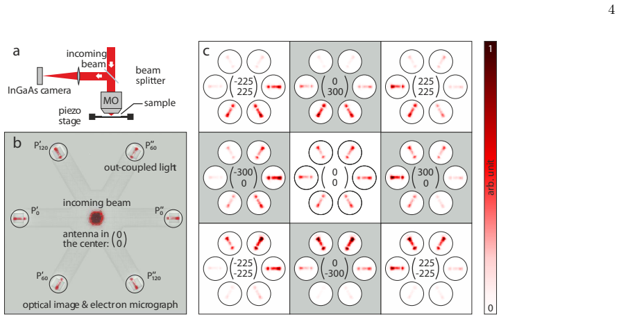
The load-bearing object is the Huygens dipole, a combination of an electric dipole and a magnetic dipole of equal strength and matching phase that emits with the maximum directionality allowed for a single dipolar source. In this device it is created by placing the silicon antenna off-axis in a tightly focused radially polarized beam, so the local field excites a longitudinal electric dipole and a transverse magnetic dipole simultaneously. The directional evanescent field of that dipole couples preferentially into specific arms of the photonic-crystal waveguide crossing. Position is read out from the directivity parameters $D_i = (P''_i - P'_i)/(P''_i + P'_i)$ for the three waveguide axes, and the linear calibration model $D = \hat{M} r + O$ with a pseudoinverse converts the three measured directivities back into coordinates $x$ and $y$.
What would settle it
Keep the piezo stage stationary while recording the six out-coupler intensities for several minutes; if the reconstructed position wanders by more than about $\pm 5$ nm, the claimed accuracy is dominated by environmental drift rather than by the calibration map. Then repeat the calibration-line scan across a range wider than $\pm 100$ nm and check whether the linear model's residuals stay below the same threshold; any systematic deviation demonstrates that the $\lambda/300$ claim is confined to the fitted window.
Extended reading notes
Core claim
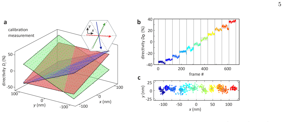
The central claim is that position information can be encoded directly in the directional emission of a single dipolar antenna: when the antenna is moved off the axis of the focused beam, the longitudinal electric and transverse magnetic field components excite electric and magnetic dipoles whose phases and amplitudes can be tuned, by choosing the 1608 nm wavelength and the roughly 260 nm radius silicon sphere, to form a Huygens dipole. That dipole scatters preferentially toward one side, and because the evanescent part of its angular spectrum is also directional, it couples asymmetrically into the six arms of the photonic-crystal crossing. The measured directivity parameters $D_0$, $D_{60}$, and $D_{120}$ vary linearly with displacement, so the three values form an overdetermined system that recovers both $x$ and $y$ through the calibration model $D = \hat{M} r + O$. In a 25 nm step line scan, each step is clearly resolved, and the reconstructed positions have standard deviations of order $\pm 5$ nm, corresponding to the claimed accuracy below $\lambda/300$.
Load-bearing premise
The load-bearing premise is that the measured directivity-to-position map stays fixed and linear after calibration; if the beam drifts, the sample moves, or the antenna leaves the $\pm 100$ nm calibrated region, the reconstructed positions inherit that error directly.
Editorial extensions
If this is right
- Position is encoded in relative waveguide intensities, so the sensor needs no long reference arms and can be fabricated on a standard silicon-on-insulator stack.
- Replacing the six tapered out-couplers with integrated photodetectors would make the whole readout on-chip, eliminating the external camera from the measurement chain.
- Because the directional-coupling pattern changes with the antenna's location, the same platform could be extended to sense rotation, wavelength, polarization, or wavefront tilt.
- The demonstrated directivity sensitivities of about $0.33$ to $0.37\,\%/\mathrm{nm}$ make nanometer-scale displacements visible to a camera, and optimizing the particle's magnetic-to-electric polarizability ratio should increase the directionality.
- At room temperature and ambient conditions, a position readout below $\lambda/300$ is directly useful for drift correction and sample stabilization in microscopy and nanometrology.
Reading between the lines
- The calibration is fitted only over a $\pm 100$ nm window, so an unstated consequence is that the advertised accuracy is confined to that range; a wider-range sensor would need a nonlinear calibration, a lookup table, or an array of antennas to avoid saturating the directionality.
- The device measures the relative position of beam and antenna, so it could equally be operated as a beam-position monitor for laser alignment; the paper does not mention this reversed use.
- The authors note that part of the reported $\pm 5$ nm scatter comes from real vibrations and drift, so the intrinsic photon-noise limit is probably lower; a stiffer mount and faster readout would likely push the repeatability toward the angstrom-level localization already shown in free-space transverse Kerker experiments.
- Their measured polarizability ratio $\alpha_m/\alpha_e \approx 0.63 e^{i0.58\pi}$ is below the ideal Huygens condition, which suggests the integrated sensitivity is not yet at the platform's ceiling; particle-size or wavelength tuning should improve the directional contrast.
Signed reviews
Editorial analysis
A structured set of objections, weighed in public.
Referee Report
Summary. The paper presents a prototype integrated photonic displacement sensor based on the position-dependent directional coupling of Huygens dipoles excited in a silicon nanoantenna placed at a six-way photonic crystal waveguide crossing. The authors support the concept with angular spectrum calculations, FDTD simulations, and a proof-of-principle experiment. A calibration raster scan (21x21 points, 10 nm steps) fits the linear model D = M r + O (Eq. 6); a subsequent line scan (11 positions, 25 nm steps, 61 frames each) reconstructs positions via the inverse of the same calibration (Eq. 8), yielding standard deviations of about 5 nm. The abstract and discussion claim a position accuracy below lambda/300 (about 5 nm at 1608 nm).
Significance. The paper is a solid proof-of-principle for chip-integrated displacement sensing using directional coupling of Huygens dipoles to photonic crystal waveguides. Its strengths include a clear physical mechanism, independent theoretical and numerical validation, a careful calibration procedure with reported confidence bounds, and a publicly available dataset via DOI. However, the headline claim conflates precision with accuracy: the reported ~5 nm standard deviation is a measure of frame-to-frame repeatability, not accuracy relative to an external displacement reference. With an appropriate reframing, the device is a meaningful step toward integrated nanophotonic displacement readout; the current claim overstates what is established.
major comments (2)
- [Quantitative analysis, Eqs. (6) and (8), Fig. 5c] The abstract and Discussion state that the device achieves a 'standard deviation of the position accuracy below λ/300'. The analysis calibrates the directivity-to-position map against piezo stage positions and then reconstructs positions from the same calibration for repeated frames. The resulting standard deviations of about ±5 nm quantify frame-to-frame repeatability (precision), not accuracy relative to an independent displacement reference. Systematic errors in the calibration matrix M and offset O, drift of the beam or sample between calibration and measurement, and nonlinearity of D(r) outside the calibrated range are not included in this estimate. The manuscript's own statement that the value 'represents only an upper bound' (last paragraph of Quantitative analysis) is consistent with a precision claim, not an accuracy claim. I request that the abstract and conclusions be reworded to 'repeatability' or 'precision', or that an independent displacement reference (e.g., an interferometric stage readout) be used to validate the calibration and justify the term 'accuracy'.
- [Quantitative analysis, Fig. 5b] The line scan in Fig. 5b uses 11 positions with 25 nm steps, spanning ±125 nm, which exceeds the calibration range of ±100 nm (21x21 raster scan with 10 nm steps, as stated in the same section). The reconstructed positions in Fig. 5c for the outermost scan points are therefore obtained by extrapolating the linear model beyond the calibrated region. The manuscript does not justify the linearity of D(r) outside ±100 nm or discuss the impact of extrapolation on the claimed resolution. This should be addressed either by restricting the claim to the calibrated range or by providing additional calibration data or a physical argument for linearity outside that range.
minor comments (5)
- [Implementation] There is a typo in the text: 'magenetic' should be 'magnetic'.
- [Fig. 3c] The position labels in each panel, such as '0 300', should be explicitly clarified as (x, y) offsets in nm; the current formatting may be ambiguous.
- [Quantitative analysis, Eq. (1)] The quantities P_i' and P_i'' are not defined explicitly. Please define them as the powers measured at the two output arms of waveguide i, or clarify the notation.
- [Methods, Eqs. (6) and (7)] The calibration matrix is denoted M in Eq. (6) but \hat{M} in Eq. (7). Please use consistent notation throughout.
- [Theoretical Concept] The sentence 'The wavelength λ in comparison to the size of the focal spot is indicated by the black bar in the upper left panel' is slightly unclear; specifying the length of the bar in the figure caption would improve readability.
Circularity Check
No significant circularity: the sensor calibration is standard practice, the Huygens-dipole coupling theory is independently derived, and the λ/300 figure is a precision estimate rather than a circular prediction.
full rationale
The paper's central physical derivation is self-contained. The angular spectrum of the Huygens dipole (Methods, Eqs. 2–5) follows from standard electric/magnetic dipole angular-spectrum formulas and independent external references; it is not defined in terms of the measured directivities. The FDTD simulation provides an independent numerical implementation of the same geometry and yields a coupling ratio (6.6) that is compared with experiment (4.5), so the directionality claim is not obtained by renaming the input. The quantitative sensor analysis is an explicit calibration: the linear map D = M r + O (Eq. 6) is fitted to a raster scan, and positions are recovered with the pseudo-inverse (Eq. 8) from a separate line-scan dataset. This is standard calibration/inversion practice, not circular reasoning, because the calibration and test measurements are distinct and the recovered positions are not asserted to follow from the calibration as a new physical prediction. The wording issue is that the reported ±5 nm standard deviations quantify repeatability/precision after calibration, not absolute accuracy against an independent displacement reference; the paper itself flags this in the Quantitative Analysis section: 'This estimate of the position accuracy, however, represents only an upper bound for the actually achievable localization accuracy, since the relatively high standard deviations are partially caused by actual variations of the particle position relative to the beam.' That is a precision-versus-accuracy caveat, not a circularity. Self-citations to prior transverse Kerker scattering work are contextual (sensitivity comparisons, linearity references [10,11,35]) and are not load-bearing: the integrated device is measured and simulated independently, and no uniqueness theorem or unverified ansatz is imported solely from the authors' prior papers. Hence no circular step is exhibited.
Assumptions & free parameters
free parameters (2)
- M matrix entries (sensitivities) =
0.33, -0.02, 0.16, 0.33, 0.06, -0.36 %/nm
- Offset vector O =
-1.75%, 2.54%, 1.85%
assumptions (4)
- standard math Vectorial diffraction theory (Richards-Wolf) describes the focused radially polarized beam field distributions used in Fig. 1a.
- domain assumption The Si nanoparticle response is dominated by electric and magnetic dipole Mie coefficients; higher-order multipoles are negligible, and the Mie phase difference compensates the beam's field phase.
- ad hoc to paper The directivity parameters are linearly dependent on position D = M r + O (Eq. 6) over the operating range.
- domain assumption The photonic crystal waveguide supports a guided TM mode at λ=1608 nm and couples the Huygens dipole evanescent field directionally.
Cite this review
Pith. "Pith review of Towards fully integrated photonic displacement sensors." pith.science (2026). https://pith.science/paper/GDYU4HLP
@misc{pith2026190904478,
  author       = {Pith},
  title        = {Pith review of: Towards fully integrated photonic displacement sensors},
  year         = {2026},
  howpublished = {\url{https://pith.science/paper/GDYU4HLP}},
  note         = {Machine review of arXiv:1909.04478}
}
abstract
The field of optical metrology with its high precision position, rotation and wavefront sensors represents the basis for lithography and high resolution microscopy. However, the on-chip integration - a task highly relevant for future nanotechnological devices - necessitates the reduction of the spatial footprint of sensing schemes by the deployment of novel concepts. A promising route towards this goal is predicated on the controllable directional emission of the fundamentally smallest emitters of light, i.e. dipoles, as an indicator. Here we realize an integrated displacement sensor based on the directional emission of Huygens dipoles excited in an individual dipolar antenna. The position of the antenna relative to the excitation field determines its directional coupling into a six-way crossing of photonic crystal waveguides. In our experimental study supported by theoretical calculations, we demonstrate the first prototype of an integrated displacement sensor with a standard deviation of the position accuracy below $\lambda$/300 at room temperature and ambient conditions.
Figures


Figures from the paper (2 more)

Reference graph
Works this paper leans on
-
[1]
Technology and applications of grating interfer- ometers in high-precision measurement
Teimel, A. Technology and applications of grating interfer- ometers in high-precision measurement. Precis. Eng. 14, 147–154 (1992)
work page 1992
- [2]
-
[3]
Berkovic, G. & Shafir, E. Optical methods for distance and displacement measurements. Adv. Opt. Photon. 4, 441 (2012)
work page 2012
-
[4]
Abbott, B. P. Observation of Gravitational Waves from a Binary Black Hole Merger. Phys. Rev. Lett. 116, 61102 (2016)
work page 2016
-
[5]
Nugent-Glandorf, L. & Perkins, T. T. Measuring 0.1-nm motion in 1 ms in an optical microscope with differen- tial back-focal-plane detection. Opt. Lett. 29, 2611–2613 (2004)
work page 2004
-
[6]
Carter, A. R. et al. Stabilization of an optical microscope to 0.1 nm in three dimensions. Appl. Opt. 46, 421–427 (2007)
work page 2007
-
[7]
Klar, T. A. & Hell, S. W. Subdiffraction resolution in far-field fluorescence microscopy. Opt. Lett. 24, 954–956 (1999)
work page 1999
-
[8]
Betzig, E. et al. Imaging intracellular fluorescent proteins at nanometer resolution. Science 313, 1642–1645 (2006)
work page 2006
Show all 45 references
-
[9]
N., Carneiro, K., Haitjema, H
Hansen, H. N., Carneiro, K., Haitjema, H. & De Chiffre, L. Dimensional micro and nano metrology. CIRP Annals - Manufacturing Technology 55, 721–743 (2006)
2006
-
[10]
& Banzer, P
Bag, A., Neugebauer, M., Wo´ zniak, P., Leuchs, G. & Banzer, P. Transverse Kerker Scattering for Angstrom Lo- calization of Nanoparticles. Phys. Rev. Lett. 121, 193902 (2018)
2018
-
[11]
& Banzer, P
Neugebauer, M., Wo´ zniak, P., Bag, A., Leuchs, G. & Banzer, P. Polarization-controlled directional scattering for nanoscopic position sensing. Nat. Commun. 7, 11286 (2016)
2016
-
[12]
Shang, W. et al. Unidirectional scattering exploited trans- verse displacement sensor with tunable measuring range. Opt. Express 27, 4944 (2019)
2019
-
[13]
Geffrin, J. et al. Magnetic and electric coherence in forward- and back-scattered electromagnetic waves by a single di- electric subwavelength sphere. Nat. Commun. 3, 1171 (2012)
2012
-
[14]
F., Zayats, A
Picardi, M. F., Zayats, A. V. & Rodr´ ıguez-Fortu˜ no, F. J. Janus and Huygens Dipoles: Near-Field Directionality Be- yond Spin-Momentum Locking. Phys. Rev. Lett. 120, 117402 (2018)
2018
-
[15]
& Giles, C
Kerker, M., Wang, D.-S. & Giles, C. L. Electromagnetic scattering by magnetic spheres. J. Opt. Soc. Am. 73, 765 (1983)
1983
-
[16]
A., Saiz, J
Garc´ ıa-C´ amara, B., de la Osa, R. A., Saiz, J. M., Gonz´ alez, F. & Moreno, F. Directionality in scattering by nanopar- ticles: Kerker’s null-scattering conditions revisited. Opt. Lett. 36, 728–730 (2011)
2011
-
[17]
Notomi, M. et al. Extremely large group-velocity dispersion of line-defect waveguides in photonic crystal slabs. Phys. Rev. Lett. 87, 253902 (2001)
2001
-
[18]
& Leuchs, G
Quabis, S., Dorn, R., Eberler, M., Gl¨ ockl, O. & Leuchs, G. Focusing light to a tighter spot. Opt. Commun. 179, 1–7 (2000)
2000
-
[19]
& Brown, T
Youngworth, K. & Brown, T. Focusing of high numerical aperture cylindrical-vector beams. Opt. Express 7, 77–87 (2000)
2000
-
[20]
& Leuchs, G
Wo´ zniak, P., Banzer, P. & Leuchs, G. Selective switch- ing of individual multipole resonances in single dielectric nanoparticles. Laser Photon. Rev. 9, 231–240 (2015)
2015
-
[21]
& Wolf, E
Richards, B. & Wolf, E. Electromagnetic Diffraction in Optical Systems. II. Structure of the Image Field in an Aplanatic System. Proc. R. Soc. A 253, 358–379 (1959)
1959
-
[22]
& Hecht, B
Novotny, L. & Hecht, B. Principles of Nano-Optics (Cam- bridge University Press, Cambridge, 2006), 2nd edn
2006
-
[23]
J., G´ omez-Medina, R
Nieto-Vesperinas, M., S´ aenz, J. J., G´ omez-Medina, R. & Chantada, L. Optical forces on small magnetodielectric particles. Opt. Express 18, 11428–11443 (2010)
2010
-
[24]
S., Bauer, T
Neugebauer, M., Eismann, J. S., Bauer, T. & Banzer, P. Magnetic and Electric Transverse Spin Density of Spatially Confined Light. Phys. Rev. X 8, 021042 (2018)
2018
-
[25]
Staude, I. et al. Tailoring directional scattering through magnetic and electric resonances in subwavelength silicon nanodisks. ACS Nano 7, 7824–7832 (2013)
2013
-
[26]
M., Curto, A
Hancu, I. M., Curto, A. G., Castro-L´ opez, M., Kuttge, M. & van Hulst, N. F. Multipolar Interference for Directed Light Emission. Nano Lett. 14, 166–171 (2014)
2014
-
[27]
Scattering and diffraction in physical optics (Wiley, 1991)
Nieto-Vesperinas, M. Scattering and diffraction in physical optics (Wiley, 1991)
1991
-
[28]
& Wolf, E
Mandel, L. & Wolf, E. Optical coherence and quantum optics (Cambridge University Press, 1995)
1995
-
[29]
& Leuchs, G
Mick, U., Banzer, P., Christiansen, S. & Leuchs, G. AFM- Based Pick-and-Place Handling of Individual Nanoparti- cles inside an SEM for the Fabrication of Plasmonic Nano- Patterns. Cleo: 2014 STu1H.1 (2014)
2014
-
[30]
Arcari, M. et al. Near-Unity Coupling Efficiency of a Quan- tum Emitter to a Photonic Crystal Waveguide. Phys. Rev. Lett. 113, 093603 (2014)
2014
-
[31]
Morichetti, F. et al. Non-invasive on-chip light observation by contactless waveguide conductivity monitoring. IEEE Journal on Selected Topics in Quantum Electronics 20, 292–301 (2014)
2014
-
[32]
Grillanda, S. et al. Non-invasive monitoring and control in silicon photonics by CMOS integrated electronics. Optica 1, 129–136 (2014)
2014
-
[33]
& Paparo, D
Marrucci, L., Manzo, C. & Paparo, D. Optical Spin-to- Orbital Angular Momentum Conversion in Inhomogeneous Anisotropic Media. Phys. Rev. Lett. 96, 163905 (2006)
2006
-
[34]
& Leuchs, G
Neugebauer, M., Bauer, T., Banzer, P. & Leuchs, G. Polar- ization Tailored Light Driven Directional Optical Nanobea- 8 con. Nano Lett. 14, 2546–2551 (2014)
2014
-
[35]
& Schmidt, C
Gittes, F. & Schmidt, C. F. Interference model for back- focal-plane displacement detection in optical tweezers. Opt. Lett. 23, 7–9 (1998)
1998
-
[36]
& Banzer, P
Neugebauer, M., Nechayev, S., Vorndran, M., Leuchs, G. & Banzer, P. Weak Measurement Enhanced Spin Hall Effect of Light for Particle Displacement Sensing. Nano Lett. 19, 422–425 (2018)
2018
-
[37]
Roy, S., Ushakova, K., van den Berg, Q., Pereira, S. F. & Urbach, H. P. Radially Polarized Light for Detection and Nanolocalization of Dielectric Particles on a Planar Substrate. Phys. Rev. Lett. 114, 103903 (2015)
2015
-
[38]
Shegai, T. et al. A bimetallic nanoantenna for directional colour routing. Nat. Commun. 2, 481 (2011)
2011
-
[39]
P., Leosson, K
Balthasar Mueller, J. P., Leosson, K. & Capasso, F. Ul- tracompact metasurface in-line polarimeter. Optica 3, 42 (2016)
2016
-
[40]
J., Griol, A
Espinosa-Soria, A., Rodr´ ıguez-Fortu˜ no, F. J., Griol, A. & Mart´ ınez, A. On-Chip Optimal Stokes Nanopolarimetry Based on Spin-Orbit Interaction of Light. Nano Lett. 17, 3139–3144 (2017)
2017
-
[41]
& Kuipers, L
le Feber, B., Rotenberg, N. & Kuipers, L. Nanophotonic control of circular dipole emission. Nat. Commun. 6, 6695 (2015)
2015
-
[42]
Tischler, N. et al. All-Optical Self-Referenced Transverse Position Sensing with Subnanometer Precision. ACS Pho- tonics 5, 3628–3633 (2018)
2018
-
[43]
& Leuchs, G
Bauer, T., Orlov, S., Peschel, U., Banzer, P. & Leuchs, G. Nanointerferometric amplitude and phase reconstruction of tightly focused vector beams. Nat. Photon. 8, 23–27 (2014)
2014
-
[44]
F., Manjavacas, A., Zayats, A
Picardi, M. F., Manjavacas, A., Zayats, A. V. & Rodr´ ıguez- Fortu˜ no, F. J. Unidirectional evanescent-wave coupling from circularly polarized electric and magnetic dipoles: An angular spectrum approach. Phys. Rev. B 95, 245416 (2017)
2017
-
[45]
ACKNOWLEDGMENT The authors gratefully acknowledge the fruitful discus- sions with Gerd Leuchs
https://doi.org/10.17630/da3abeab-d8a6-4297-aa52- 680079a36c19. ACKNOWLEDGMENT The authors gratefully acknowledge the fruitful discus- sions with Gerd Leuchs. This project has received funding from the European Unions Horizon 2020 research and in- novation programme under the ...
Reviewed August 14, 2026 · model on record in the stance chip above.
Discussion (0). Continue with ORCID to comment.