REVIEW 2 major objections 5 minor 1 cited by
Switching topological states via uniaxial strain in 2D materials
T0 review · 2 major / 5 minor · reviewed 2026-08-05 · deepseek-v4-flash
Pith's one-line read The central claim is that uniaxial strain can switch the Chern number of monolayer MnBi2S2Te2 from C=2 to C=1 for strain along the zigzag axis and to C=0 for strain along the armchair axis, with the bulk band gap closing and reopening at ea
desk verdict Uniaxial strain can switch the Chern number in MnBi2S2Te2, but the fixed Poisson ratio makes the exact phase boundaries a prediction rather than a robust derivation. read the letter →
The pith
A machine-rendered reading of the paper's core claim, the machinery that carries it, and where it could break.
The reading
What carries the argument
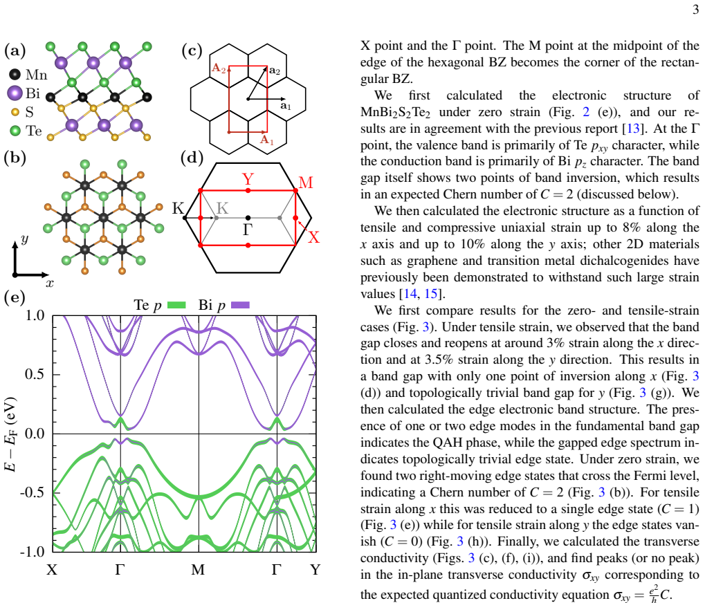
The central object is the doubly inverted band gap at the Gamma point of monolayer MnBi2S2Te2, carried by Bi p-orbital and Te p-orbital states with opposite parity, which gives a Chern number of C=2. Uniaxial strain is modeled in a rectangular 1x√3 supercell, with the transverse lattice vector scaled by a fixed Poisson ratio of -0.3. The mechanism works because the Janus structure breaks inversion symmetry, allowing the two band inversions to unwind cleanly rather than merely metallize. The paper uses Wannier-interpolated tight-binding models to count edge modes in a slab geometry and to compute the anomalous Hall conductivity, which together identify the Chern number at each strain value.
What would settle it
Recompute the band structure of MnBi2S2Te2 under uniaxial strain with the transverse lattice vector relaxed until the transverse stress vanishes, or measure the material's actual Poisson ratio. If the C=2 to C=1 gap reopening along x or the C=2 to C=0 reopening along y disappears, the reported switching is an artifact of the assumed Poisson ratio. Experimentally, measure the Hall conductivity of a strained flake: the quantized plateau should step from 2e^2/h to e^2/h or to zero as strain crosses the critical values.
Extended reading notes
Core claim
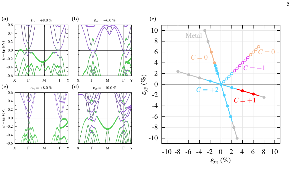
The paper's central discovery is that in the Janus monolayer MnBi2S2Te2, which has a doubly inverted band gap and two chiral edge modes (C=2), uniaxial tensile strain unwinds those inversions in a direction-dependent way. Around 3% strain along the zigzag axis the gap closes and reopens with a single inversion, leaving one edge mode (C=1); around 3.5% strain along the armchair axis it closes and reopens with no inversion, leaving no edge mode (C=0). The paper confirms these assignments by counting Fermi-level-crossing edge modes in slab tight-binding calculations and by computing the anomalous Hall conductivity, which plateaus at (e^2/h)C. Larger strain drives the system metallic. Combining
Load-bearing premise
The calculations set the transverse lattice spacing under uniaxial strain by assuming a Poisson ratio of -0.3, a typical value for 2D materials, instead of relaxing it to zero transverse stress for this specific compound.
Editorial extensions
If this is right
- Strain becomes a reversible, external control knob for quantized Hall conduction: a single flake can be toggled between C=2, C=1, and C=0 by stretching along different in-plane axes.
- A sample under a strain gradient should contain a one-dimensional dissipationless edge mode at the line where the band gap closes, requiring no physical cut, magnetic domain wall, or thickness step.
- The proposed topological transistor and topological current switch have concrete operating principles: current is blocked or rerouted when a strained region becomes trivial or hosts an internal conducting boundary.
- The combined uniaxial and biaxial phase diagram shows that strain alone can navigate all accessible topological phases of MnBi2S2Te2, including C=-1 and a metallic phase, making the phase space continuously tunable.
- The contrast with MnBi2Te4, which only metallizes under uniaxial strain, identifies inversion-symmetry breaking as the likely condition that lets the gap close and reopen as a trivial insulator.
Reading between the lines
- A testable extension: other Janus magnetic topological insulators, or heterostructures with asymmetric chalcogen layers, should show similar strain-uninversion behavior if the uninverted gap can be restored without metallizing.
- The x/y asymmetry suggests the two band inversions couple to different orbital characters, so tuning the S/Te ratio or layer stacking could widen the strain window of the C=1 phase.
- If a strain boundary carries a quantized chiral mode, nonlocal transport across a patterned strain profile should show conductance steps in units of e^2/h, with the sign determined by the Chern-number difference.
- Because the phase boundaries depend on the transverse lattice response, substrate clamping or encapsulation could serve as an additional experimental tuning knob by changing the effective Poisson ratio.
Signed reviews
Editorial analysis
A structured set of objections, weighed in public.
Referee Report
Summary. The manuscript uses DFT with a standard VASP/Wannier pipeline to study strain-induced topological transitions in monolayer MnBi2S2Te2. Under zero strain the material is predicted to be a C=2 Chern insulator. The authors report that uniaxial tensile strain along x closes and reopens the gap, yielding a C=1 phase, while strain along y yields a C=0 trivial insulator. They also report metallic behavior at larger strains and combine these results with earlier biaxial-strain data from Ref. [13] to construct a strain-phase diagram. The paper proposes that a boundary between strained and unstrained regions can act as a new dissipationless edge, with possible device applications as a topological transistor or switch. The paper also reports unsuccessful attempts on MnBi2Te4 and V2WS4, which are placed in the Supplementary Materials.
Significance. If the predicted C=2 → C=1 → C=0 switching is robust, the paper would establish a concrete mechanism for mechanically controlling quantum anomalous Hall edge conduction in a 2D material, and would introduce a strain-domain topological boundary as a designable element. The strengths are the use of multiple independent diagnostics — bulk gap closing/reopening, edge-mode counting, and anomalous Hall conductivity plateaus — and the fact that the Chern numbers are computed directly from the Wannier Hamiltonian rather than fitted to a target. The predicted phase diagram is falsifiable by transport measurements under controlled uniaxial stress. The main weakness is that the entire switching sequence is computed along a prescribed strain path with a fixed, unvalidated transverse lattice response, which limits the current strength of the quantitative claim.
major comments (2)
- [Results, first paragraph; Fig. 4(e)] The reported topological switching is computed along a strain path in which the transverse lattice vector is scaled by a Poisson ratio of -0.3, described only as 'a typical value for 2D materials.' This is a load-bearing structural assumption for a Janus monolayer whose actual Poisson response may be anisotropic and strain-dependent. The gap-closing strains (~3% and ~3.5%) and the existence of the C=1 and C=0 phases in Fig. 4(e) depend on the full lattice geometry. A different transverse contraction could shift those thresholds, narrow or eliminate the C=1 window, or change the metal/C=0 boundary. I ask the authors to remove this assumption by either (i) computing the transverse lattice vector under zero in-plane stress for uniaxial loading, or (ii) scanning the Poisson ratio over a plausible range (e.g., 0.1–0.5) and showing that the reported Chern sequence and edge-mode counts persist.
- [Fig. 4(e) and text near 'around 3%'] The phase diagram combines a small number of new uniaxial calculations with prior biaxial points from Ref. [13], and the critical strains are given only approximately. The boundaries in Fig. 4(e) appear to be interpolated, and the reader cannot determine whether the C=1 phase occupies a wide enough strain window to be experimentally relevant or whether the C=0 phase is robust over an extended range. Please provide a table listing every computed strain value, the corresponding Chern number (or metal/insulator status), and the method used to assign it, and add points in the immediate vicinity of the transitions. This is important because the claim of clean switching rests on the sequence and ordering of these phases.
minor comments (5)
- [Abstract] In the abstract, 'MnBi2S2T2' should be 'MnBi2S2Te2'.
- [Results, first paragraph] The use of the phrase 'Poisson ratio of -0.3' is confusing because the conventional Poisson ratio is positive for most 2D materials and is defined as -ε_transverse/ε_axial. Please define the convention explicitly (e.g., ε_transverse = -ν ε_axial) and state that the value used is ν=0.3 in that convention, or correct the sign.
- [Fig. 4(e) caption] The caption should clarify that the phase boundaries are guides to the eye, since the filled and empty circles represent discrete calculations, and should specify which parameters are varied along the axes (applied strain along x and y).
- [Discussion] The statement that the proposed strain-boundary edge mode is a consequence of the difference in Chern numbers is correct, but it would be useful to state explicitly that the bulk gap must remain finite on both sides of the boundary, as also illustrated in Fig. 1(a).
- [Title/Introduction] The title and abstract say '2D materials,' but the positive demonstration is for a single material, MnBi2S2Te2, while two other materials are reported to show metallization rather than a topological switch. The scope of the claim could be qualified in the title or abstract to avoid overgeneralization.
Circularity Check
No significant circularity: Chern numbers are computed from first-principles Wannier Hamiltonians without fitting to target topological invariants; the only questionable input (Poisson ratio) is an assumption, not a fitted output.
full rationale
The central derivation chain is DFT → Wannier tight-binding → edge-state count and anomalous Hall conductivity. The Chern numbers C=2, C=1, C=0 are obtained by direct computation of topological invariants from the Wannier Hamiltonian; no parameter is fitted to reproduce a desired Chern number. The prior biaxial data from Ref. [13] are used as independent input to complete the phase diagram, not as a substitute for the uniaxial calculations. The self-citations (Refs. [20,21]) appear only in the Discussion as context for Janus polarization/substrate coupling and do not support the strain-switching claim. The Poisson ratio -0.3 used to set the transverse lattice vector is an external assumption about the strain path, not an output fitted to the target phases; while this is a correctness risk, it is not circularity. The topological statement that boundaries between regions of different C host edge modes is a standard theorem, not a self-citation. Therefore no step in the paper's derivation reduces by construction to its inputs.
Assumptions & free parameters
free parameters (1)
- Poisson ratio for transverse lattice strain =
-0.3
assumptions (3)
- standard math Bulk-boundary correspondence: regions with different Chern numbers must be separated by a gap closing and host edge modes.
- domain assumption PBE + SOC + DFT-D3 provides a qualitatively correct description of the band inversion in MnBi2S2Te2.
- domain assumption The Wannier tight-binding model faithfully reproduces the DFT band structure in the energy window of interest.
Cite this review
Pith. "Pith review of Switching topological states via uniaxial strain in 2D materials." pith.science (2026). https://pith.science/paper/GKOMDD6L
@misc{pith2026250903854,
  author       = {Pith},
  title        = {Pith review of: Switching topological states via uniaxial strain in 2D materials},
  year         = {2026},
  howpublished = {\url{https://pith.science/paper/GKOMDD6L}},
  note         = {Machine review of arXiv:2509.03854}
}
read the original abstract
In topological materials, dissipationless edge currents are protected against local defect scattering by the bulk inverted band structure and band gap. We propose that large uniaxial strain can effectively switch a 2D Chern insulator to a topologically trivial state. Further, we suggest that the boundary between strained and unstrained regions of a sample can act as a new edge for dissipationless current flow. Using density functional theory (DFT) calculations we demonstrate the strain-tunability of the monolayer MnBi2S2T2 band structure and the switching of the Chern number. We combine uniaxial and biaxial strain results to map out the strain-tuned topological phase diagram.
Figures


Figures from the paper (1 more)
Forward citations
Cited by 1 Pith paper
-
Engineering Topology by Design in Two-dimensional Materials
Van der Waals interface engineering (stacking, twist, light, functionalization) can create 2D topological insulator phases even from topologically trivial constituents, expanding the usable materials landscape.
Reference graph
Works this paper leans on
-
[13]
Y . Li, S. Xu, J. Wang, C. Wang, B. Yang, H. Lin, W. Duan, and B. Huang, Proc. Natl. Acad. Sci. 119, e2122952119 (2022)
work page 2022
-
[1]
Vanderbilt, Berry Phases in Electronic Structure Theory: Electric Polarization, Orbital Magnetization and Topological Insulators (Cambridge University Press, 2018)
D. Vanderbilt, Berry Phases in Electronic Structure Theory: Electric Polarization, Orbital Magnetization and Topological Insulators (Cambridge University Press, 2018)
2018
- [2]
-
[3]
J. G. Checkelsky, R. Yoshimi, A. Tsukazaki, K. S. Takahashi, Y . Kozuka, J. Falson, M. Kawasaki, and Y . Tokura, Nat. Phys. 10, 731 (2014)
work page 2014
- [4]
-
[5]
Y . Deng, Y . Yu, M. Z. Shi, Z. Guo, Z. Xu, J. Wang, X. H. Chen, and Y . Zhang, Science367, 895 (2020)
work page 2020
-
[6]
C. Liu, Y . Wang, H. Li, Y . Wu, Y . Li, J. Li, K. He, Y . Xu, J. Zhang, and Y . Wang, Nat. Mater.19, 522 (2020)
work page 2020
-
[7]
J. Ge, Y . Liu, J. Li, H. Li, T. Luo, Y . Wu, Y . Xu, and J. Wang, Natl. Sci. Rev. 7, 1280 (2020)
work page 2020
Show all 29 references
-
[8]
J. Ning, Y . Zhu, J. Kidd, Y . Guan, Y . Wang, Z. Mao, and J. Sun, npj Comput. Mater. 6, 157 (2020)
2020
-
[9]
Bhattarai and T
R. Bhattarai and T. D. Rhone, ACS Appl. Mater. Interfaces 16, 60856 (2024)
2024
-
[10]
Yasuda, M
K. Yasuda, M. Mogi, R. Yoshimi, A. Tsukazaki, K. Takahashi, M. Kawasaki, F. Kagawa, and Y . Tokura, Science 358, 1311 (2017)
2017
-
[11]
Ovchinnikov, J
D. Ovchinnikov, J. Cai, Z. Lin, Z. Fei, Z. Liu, Y .-T. Cui, D. H. Cobden, J.-H. Chu, C.-Z. Chang, D. Xiao, J. Yan, and X. Xu, Nat. Commun. 13, 5967 (2022)
2022
-
[12]
Jiang, H
Y . Jiang, H. Wang, K. Bao, Z. Liu, and J. Wang, Phys. Rev. Lett. 132 (2024)
2024
-
[14]
C. Lee, X. Wei, J. W. Kysar, and J. Hone, Science 321, 385 (2008)
2008
-
[15]
Rold ´an, A
R. Rold ´an, A. Castellanos-Gomez, E. Cappelluti, and F. Guinea, J. Phys.: Condens. Matter 27, 313201 (2015)
2015
-
[16]
S. Li, T. Liu, C. Liu, Y . Wang, H.-Z. Lu, and X. Xie, Natl. Sci. Rev. 11, nwac296 (2024)
2024
-
[17]
Inoue, M
H. Inoue, M. Han, M. Hu, T. Suzuki, J. Liu, and J. G. Checkel- sky, Phys. Rev. Mater.3, 101202 (2019)
2019
-
[18]
R. K. Defo, S. Fang, S. N. Shirodkar, G. A. Tritsaris, A. Di- moulas, and E. Kaxiras, Phys. Rev. B 94, 155310 (2016)
2016
-
[19]
Zhang, Y
L. Zhang, Y . Xia, X. Li, L. Li, X. Fu, J. Cheng, and R. Pan, J. Appl. Phys. 131 (2022)
2022
-
[20]
Zhang, Y
K. Zhang, Y . Guo, Q. Ji, A.-Y . Lu, C. Su, H. Wang, A. A. Puret- zky, D. B. Geohegan, X. Qian, S. Fang, et al. , J. Am. Chem. Soc. 142, 17499 (2020)
2020
-
[21]
Zhang, Y
K. Zhang, Y . Guo, D. T. Larson, Z. Zhu, S. Fang, E. Kaxiras, J. Kong, and S. Huang, ACS Nano 15, 14394 (2021)
2021
-
[22]
Zhang, Y
Y . Zhang, Y . Wang, W. Yang, H. Zhang, and J. Jia, Phys. Chem. Chem. Phys. 25, 28189 (2023)
2023
-
[23]
Mutch, W.-C
J. Mutch, W.-C. Chen, P. Went, T. Qian, I. Z. Wilson, A. An- dreev, C.-C. Chen, and J.-H. Chu, Sci. Adv.5, eaav9771 (2019)
2019
-
[24]
Kresse and J
G. Kresse and J. Furthm ¨uller, Comput. Mater. Sci.6, 15 (1996)
1996
-
[25]
J. P. Perdew, K. Burke, and M. Ernzerhof, Phys. Rev. Lett. 77, 3865 (1996)
1996
-
[26]
P. E. Bl ¨ochl, Phys. Rev. B 50, 17953 (1994)
1994
-
[27]
Grimme, J
S. Grimme, J. Antony, S. Ehrlich, and H. Krieg, J. Chem. Phys. 132, 154104 (2010)
2010
-
[28]
A. A. Mostofi, J. R. Yates, Y .-S. Lee, I. Souza, D. Vanderbilt, and N. Marzari, Comput. Phys. Commun. 178, 685 (2008)
2008
-
[29]
Q. Wu, S. Zhang, H.-F. Song, M. Troyer, and A. A. Soluyanov, Comput. Phys. Commun. 224, 405 (2018)
2018
Reviewed August 5, 2026 · model on record in the stance chip above.
Discussion (0). Continue with ORCID to comment.