REVIEW 5 minor 27 references
Third method for generation of spectral holes in chiral sculptured thin films
T0 review · 0 major / 5 minor · reviewed 2026-08-14 · deepseek-v4-flash
Pith's one-line read A two-section chiral film with swapped dielectric constants matches the transfer matrix of a 90° twist-defect film, yielding both spectral-hole types.
desk verdict A clean algebraic identity that genuinely adds a third way to make spectral holes in chiral STFs; the only real soft spot is whether a material pair satisfying the conditions exists. read the letter →
The pith
A machine-rendered reading of the paper's core claim, the machinery that carries it, and where it could break.
The reading
What carries the argument
The key machinery is the 4×4 transfer-matrix formulation for axially excited chiral STFs. Each section is described by a matrix [P_j] whose nonzero entries depend only on the half-period Ω, handedness h, wavelength, and two permittivity quantities: ε_cj and the derived ε̃_dj = ε_aj ε_bj / (ε_aj cos²χ_j + ε_bj sin²χ_j). The pseudoisotropic angle for a columnar film is exactly the tilt χ at which ε_c = ε̃_d, and this concept anchors the fabrication strategy. The load-bearing step is the similarity relation [P_2] = [B(π/2)][P_1][B(π/2)]^{-1} under the swap conditions (8); this lets the full device matrix be written as two half-thickness matrices separated by a rotation [B(π/2)], which is the same algebraic structure as a central 90° twist defect. That algebraic identity is what transfers all spectral-hole properties from the twist-defect device to the two-section film.
What would settle it
Fabricate or simulate with realistic material data a two-section chiral STF satisfying the swap condition at a design wavelength, illuminate at normal incidence, and record the co-polarized remittances: if no co-handed reflection hole appears at the Bragg-region center for moderate thickness and no cross-handed transmission hole appears for larger thickness, the claimed equivalence is not realized in practice.
Extended reading notes
Core claim
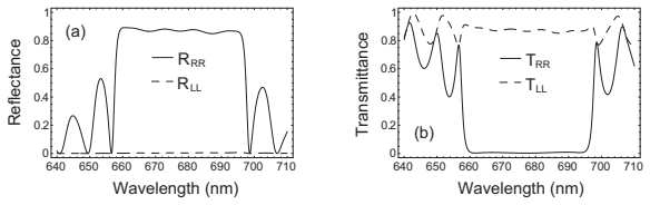
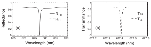
The central discovery is the matrix identity [P_2] = [B(π/2)][P_1][B(π/2)]^{-1}, which holds whenever the two sections of a two-section chiral STF satisfy ε_c1 = ε̃_d2 and ε̃_d1 = ε_c2, with ε̃_dj = ε_aj ε_bj / (ε_aj cos²χ_j + ε_bj sin²χ_j). Under this condition the transfer matrix [M] = exp(i[P_2]D/2) exp(i[P_1]D/2) becomes [B(π/2)] exp(i[P_1]D/2) [B(π/2)]^{-1} exp(i[P_1]D/2), the same algebraic form as a chiral STF with a central 90° twist defect. Consequently, for axially incident plane waves the two-section film reproduces the twist-defect film's remittance spectra: a co-handed reflection hole appears at the center of the Bragg regime for relatively small D, and it is replaced by a cross-handed transmission hole as D increases. The equivalence is electromagnetic but not exact: the z-directed field components inside the device generally differ, so the two devices are not identical in their internal field structure.
Load-bearing premise
The entire design depends on there being two real materials that can be vapor-deposited into chiral columns with the same period and handedness while their dielectric parameters satisfy the swap condition; the paper offers only sparse prior measurements, not a demonstrated device, as evidence this can be done.
Editorial extensions
If this is right
- If the two-section film satisfies (8), it exhibits a co-handed reflection hole at the center of the Bragg regime for relatively small thickness, exactly as a 90° twist-defect film does.
- For larger thickness, that reflection hole disappears and is replaced by a cross-handed transmission hole, matching the known thickness-dependent behavior of defect-containing chiral STFs.
- The method is incompatible with a single evaporant: measured columnar-film data show ε_c + ε̃_d rises monotonically with deposition angle, so one material deposited at two angles cannot satisfy (8).
- Two cholesteric liquid crystals cannot serve as the two sections because their tilt is zero and rodlike molecular shape enforces ε̃_d > ε_c; pairing a single-material STF section with a CLC section could in principle satisfy (8).
- Because the spectral-hole bandwidths are tiny, dispersion of the permittivity scalars can be neglected when designing the device over the operating band.
Reading between the lines
- One untested extension is whether the same similarity argument can position the spectral hole at an arbitrary wavelength within the Bragg regime by seeking two-section parameter relations that mimic a twist defect of angle other than 90°; the paper's identity is specifically for 90°, so such a generalization would be new.
- Because the internal z-directed field distributions of the two equivalent devices differ, measuring absorption or near-field profiles in a lossy realization could distinguish which electromagnetic construction is actually present, providing a diagnostic test of the equivalence beyond far-field remittances.
- The pseudoisotropic-angle calibration used here could be converted into a practical design rule: if manufacturers tabulate χ_pi and the sum ε_c + ε̃_d for candidate evaporants at the operating wavelength, a suitable material pair for this method could be identified without fabricating a test device first.
Signed reviews
Editorial analysis
A structured set of objections, weighed in public.
Referee Report
Summary. This paper proposes a third mechanism, beyond central layer defects and twist defects, for generating circular-polarization-sensitive spectral holes in periodic structurally chiral materials. The device is a two-section chiral sculptured thin film in which both sections share the same structural half-period and handedness but differ in their reference permittivity scalars. The central result is that if the constitutive parameters satisfy ϵc1 = ϵ~d2 and ϵ~d1 = ϵc2, then the second-section matrix [P2] is similar to [P1] via a 90° rotation, so the total transfer matrix reduces exactly to that of a chiral STF with a central 90° twist defect. The paper verifies the predicted co-handed reflection hole for small total thickness and cross-handed transmission hole for larger thickness in numerical examples, and it discusses fabrication feasibility based on the pseudoisotropy of columnar thin films.
Significance. The result is significant because it offers a distinct design route to spectral holes that avoids the practical difficulty of physically rotating one half of the film or inserting a homogeneous defect layer. The algebraic derivation is clean and parameter-free: the equivalence follows solely from condition (8) and is benchmarked against the known twist-defect transfer matrix of reference [8]. The numerical examples in Figures 2 and 3 confirm the expected spectral holes. The main caveat is that the paper does not identify a concrete material pair satisfying (8), and the dispersion of the constitutive scalars is asserted to be negligible without a quantitative bound; these are implementation concerns that do not undermine the mathematical equivalence, which is the paper's core contribution.
minor comments (5)
- [Abstract] The word 'highy' in the abstract should be 'highly'.
- [Section 3] The sentence 'The bandwidths of the spectral holes are so small that dispersion of the constitutive scalars ϵa,b,c can be ignored in most instances' is an assertion without a quantitative tolerance; since condition (8) must hold across the hole bandwidth for the equivalence to be exact, a criterion such as |d(ϵc−ϵ~d)/dλ|·Δλ ≪ |ϵc−ϵ~d| would make the claim more precise.
- [Section 3] The feasibility argument relies on refs. [22,24] and on a personal communication [25] to infer the dependence of the pseudoisotropic angle on deposition conditions; adding a concrete candidate material pair or deposition recipe, or at least a more detailed table of reported values, would strengthen the technological-feasibility section.
- [References] Reference [14] is a book chapter that is marked 'to be published in Jan. 2005'; since the book appeared well before this manuscript, the citation should be updated to the published volume.
- [Figures 2 and 3] The wavelength axes in Figure 3 differ between panels (a) and (b); adding a vertical marker at the hole wavelength would help the reader connect the reflection hole to the transmission hole.
Circularity Check
No significant circularity: the transfer-matrix equivalence is derived algebraically in Eqs. (8)-(10), with forward-model spectra, not fitted parameters.
full rationale
The paper's central claim is an algebraic equivalence derived entirely within the manuscript: substituting conditions (8) into the matrix (7) yields the conjugation identity (9), so the two-section transfer matrix (6) reduces to (10). No parameter is fitted to a target spectrum; the conditions are chosen to force the algebra, and the illustrative spectra in Figures 2 and 3 are forward computations from those conditions. The citation to [8] identifies the resulting matrix as that of a 90-degree twist defect, but equation (10) already displays this form directly, and the numerical examples independently confirm the expected spectral-hole behavior. The feasibility discussion involving pseudoisotropy and refs. [22,24,25] is an implementation concern, not a circular step. The footnote that the two devices differ in their z-directed fields is an honest limitation but does not affect the claimed equivalence for normally incident plane waves. Overall, the derivation is self-contained and not circular.
Assumptions & free parameters
free parameters (5)
- Example reference permittivity scalars ϵc1 = ϵ~d2 =
2.72
- Example permittivity scalars ϵ~d1 = ϵc2 =
3.02
- Structural half-period Ω =
200 nm
- Total device thickness D =
60Ω and 180Ω
- Structural handedness h =
1 (right-handed)
assumptions (7)
- domain assumption The constitutive model (1) with reference permittivity scalars ϵa,b,c and tilt angle χ accurately describes both sections of the proposed STF.
- standard math The transfer-matrix boundary-value method of refs [14,18] is valid.
- standard math The matrix identity exp(B A B^{-1}) = B exp(A) B^{-1} holds for the matrices here.
- domain assumption Excitation of Voigt waves can be neglected for the parameter regimes considered.
- domain assumption Dispersion of the constitutive scalars can be ignored over the narrow spectral-hole bandwidths.
- domain assumption A central 90-degree twist defect in a chiral STF produces the two spectral-hole types described in refs [8,10-12].
- domain assumption The interface at z = D/2 is abrupt, with no additional interfacial layer beyond the two sections.
Cite this review
Pith. "Pith review of Third method for generation of spectral holes in chiral sculptured thin films." pith.science (2026). https://pith.science/paper/HGRTIOTK
@misc{pith2026190806249,
  author       = {Pith},
  title        = {Pith review of: Third method for generation of spectral holes in chiral sculptured thin films},
  year         = {2026},
  howpublished = {\url{https://pith.science/paper/HGRTIOTK}},
  note         = {Machine review of arXiv:1908.06249}
}
read the original abstract
The introduction of either a central layer defect or a central twist defect in a periodic structurally chiral material generates circular-polarization-sensitive spectral holes in the remittance spectrums for normally incident plane waves. We propose and theoretically establish here the third method to generate such spectral holes using two-section chiral sculptured thin films (STFs). Both sections of the proposed device have the same periodicity and handedness, but their dielectric properties are different and related in a specific way. The concept of pseudoisotropy is highly relevant for the production of the proposed device.
Figures

Reference graph
Works this paper leans on
-
[8]
I. J. Hodgkinson, Q. H. Wu, K. E. Thorn, A. Lakhtakia, M. W. McCall, Opt. Com- mun. 184 (2000) 57
work page 2000
-
[1]
H. A. Haus, C. V. Shank, IEEE J. Quantum Electron. 12 (1976) 352. 8
work page 1976
-
[2]
G. P. Agrawal, N. K. Dutta, Semiconductor Lasers, Van Nostrand Reinhold, New York, 1993 (Chap. 7)
work page 1993
-
[3]
G. P. Agrawal, S. Radic, IEEE Photon. Technol. Lett. 6 (1994) 995
work page 1994
- [4]
- [5]
-
[6]
I. J. Hodgkinson, Q. h. Wu, A. Lakhtakia, M. W. McCall, Opt. Commun. 177 (2000) 79
work page 2000
-
[7]
Y.–C. Yang, C.–S. Kee, J.–E. Kim, H. Y. Park, J.–C. Lee, Y.–J. Jeon, Phys. Rev. B 60 (1999) 6852
work page 1999
Show all 27 references
-
[9]
V. I. Kopp, A. Z. Genack, U.S. Patent 6 396 859, 2002
2002
-
[10]
V. I. Kopp, A. Z. Genack, Phys. Rev. Lett. 89 (2002) 033901
2002
-
[11]
F. Wang, A. Lakhtakia, Opt. Commun. 215 (2003) 79
2003
-
[12]
I. J. Hodgkinson, Q. h. Wu, L. De Silva, M. Arnold, M. W. McCall, A. Lakhtakia, Phys. Rev. Lett. 91 (2003) 223903
2003
-
[13]
Lakhtakia, V
A. Lakhtakia, V. C. Venugopal, M. W. McCall, Opt. Commun. 177 (2003) 57
2003
-
[14]
Lakhtakia, R
A. Lakhtakia, R. Messier, Sculptured Thin Films: Nanoengineered Morphology and Optics, SPIE Press, Bellingham, WA, USA, 2005 (Chap. 10), to be published in Jan. 2005
2005
-
[15]
Schmidtke, W
J. Schmidtke, W. Stille, Eur. Phys. J. E 12 (2003) 553
2003
-
[16]
Abdulhalim, Europhys
I. Abdulhalim, Europhys. Lett. 48 (1999) 177. 9
1999
-
[17]
Lakhtakia, W
A. Lakhtakia, W. S. Weiglhofer, J. Opt. A: Pure Appl. Opt. 2 (2000) 107
2000
-
[18]
V. C. Venugopal, A. Lakhtakia, Proc. R. Soc. Lond. A 454 (1998) 1535
1998
-
[19]
Lakhtakia, Opt
A. Lakhtakia, Opt. Commun. 157 (1998) 193
1998
-
[20]
Lakhtakia, J
A. Lakhtakia, J. Phys. D: Appl. Phys. 31 (1998) 235
1998
-
[21]
I. J. Hodgkinson, Q. h. Wu, M. Arnold, M. W. McCall, A. Lakhtakia, Opt. Commun. 210 (2002) 201
2002
-
[22]
I. J. Hodgkinson, Q. H. Wu, J. Hazel, Appl. Opt. 37 (1998) 2653
1998
-
[23]
Messier, A
R. Messier, A. Lakhtakia, Mater. Res. Innov. 2 (1999) 217
1999
-
[24]
Lakhtakia, Microw
A. Lakhtakia, Microw. Opt. Technol. Lett. 34 (2002) 367
2002
-
[25]
Messier, personal communication to A
R. Messier, personal communication to A. Lakhtakia (2004)
2004
-
[26]
P. G. de Gennes, J. Prost, The Physics of Liquid Crystals, Clarendon Press, Oxford, UK, 1993 (Chap. 4). 10 640 650 660 670 680 690 700 710 0 0.2 0.4 0.6 0.8 1 640 650 660 670 680 690 700 710 0 0.2 0.4 0.6 0.8 1 Reflectance Wavelength (nm) (a) (b) Transmittance Wavelength (nm) ...
1993
-
[677]
2 677. 3 677. 4 677. 5 677. 6 Wavelength (nm)Wavelength (nm) Transmittance Reflectance(a) (b) RRR RLL TRR TLL 0 0.2 0.4 0.6 0.8 1 Figure 3: Spectrums of (a) reflectances RRR and RLL and (b) transmittances TRR and TLL, computed for a structurally right–handed, two–section chiral...
Reviewed August 14, 2026 · model on record in the stance chip above.
Discussion (0). Continue with ORCID to comment.