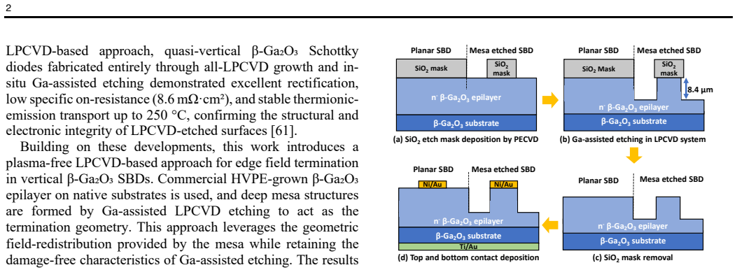
Vertical β-Ga₂O₃ Schottky Diodes with Deep-Etch Field Termination using Plasma-free Ga-assisted Etching
Pith reviewed 2026-06-30 08:31 UTC · model grok-4.3
The pith
Deep-etched mesas formed by Ga-assisted plasma-free etching raise breakdown voltage in β-Ga₂O₃ Schottky diodes from 287 V to 500 V while preserving forward characteristics.
A machine-rendered reading of the paper's core claim, the machinery that carries it, and where it could break.
Core claim
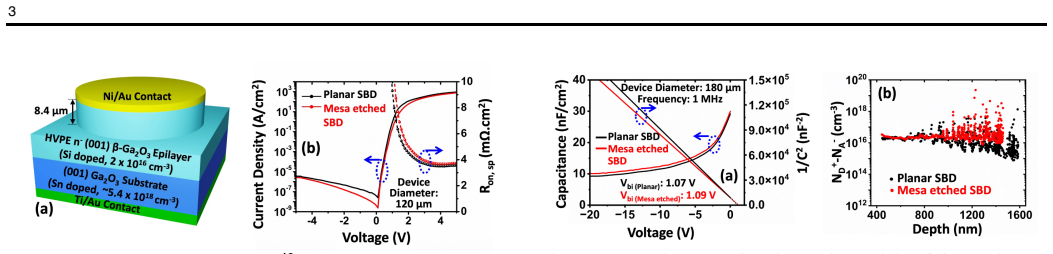
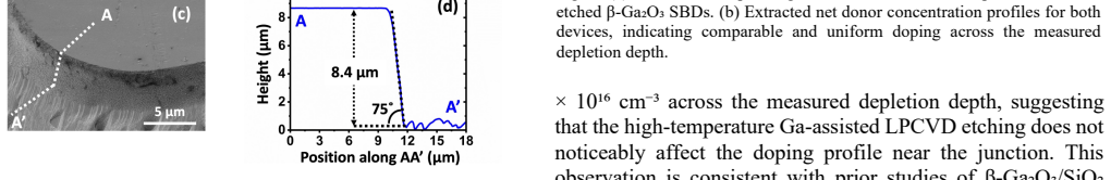
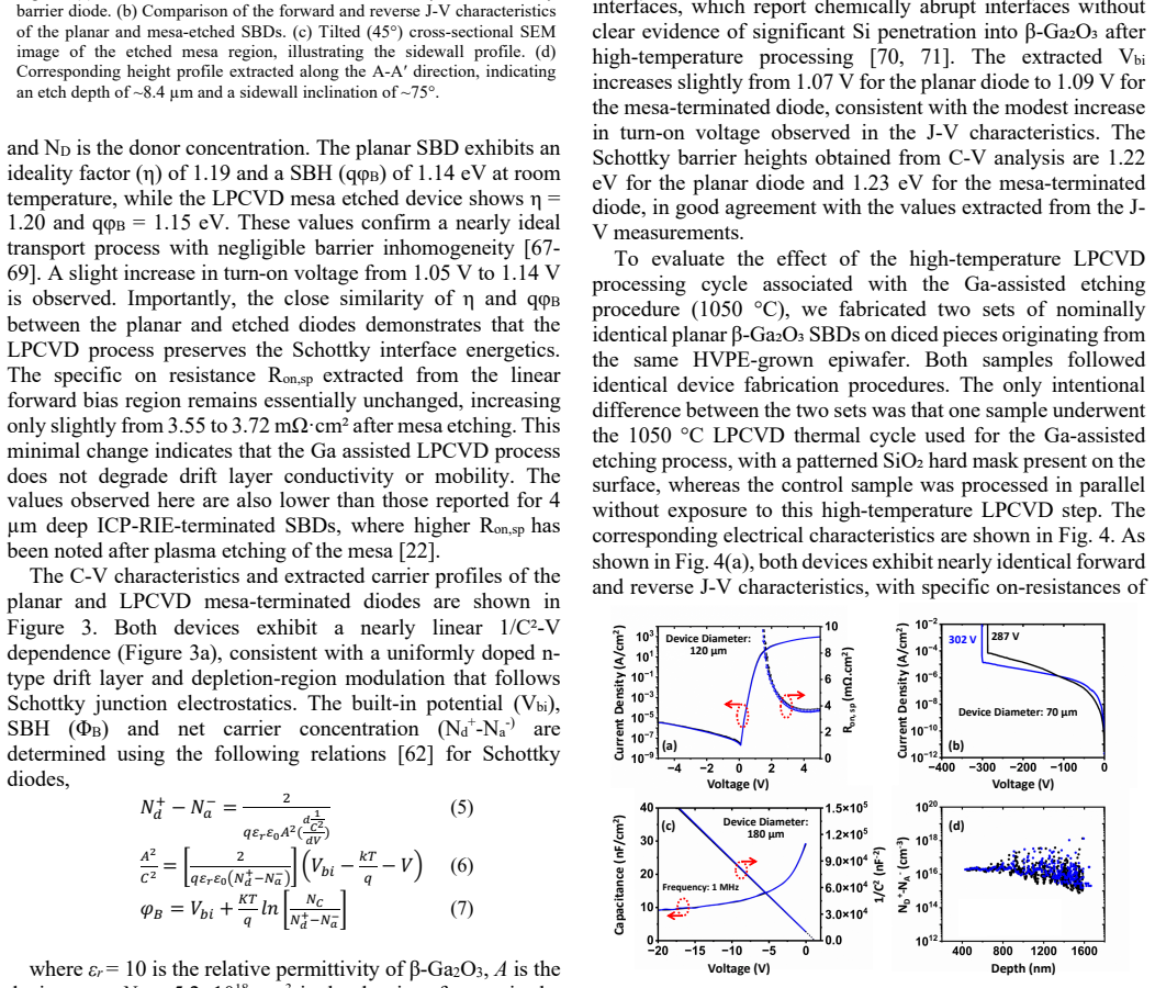
The authors demonstrate that deep-etch field termination using Ga-assisted plasma-free etching increases the breakdown voltage of β-Ga₂O₃ Schottky barrier diodes from 287 V to 500 V. The etched devices retain a turn-on voltage of 1.14 V, Schottky barrier height near 1.15–1.23 eV, ideality factor of 1.20, and specific on-resistance of 3.72 mΩ·cm², matching unetched planar references. Temperature sweeps confirm thermionic-emission transport with rectification above 10^5 at 250 °C and simulations show electric-field suppression at the anode edge.
What carries the argument
The deep-etched mesa structure produced by thermally activated Ga-assisted plasma-free etching, which geometrically redistributes the electric field to suppress crowding at the anode edge.
If this is right
- The same etch process can be applied to other vertical β-Ga₂O₃ power devices to reach higher blocking voltages.
- Integration into existing LPCVD tools eliminates the need for separate plasma-etch equipment.
- Stable high-temperature behavior supports use in environments up to at least 250 °C.
- Uniform post-etch doping profiles enable predictable device scaling.
Where Pith is reading between the lines
- The technique may extend to other wide-bandgap semiconductors that require deep field-termination structures.
- Combining the mesas with additional edge-termination layers could push breakdown voltages higher still.
- Direct comparison of long-term reliability between etched and unetched devices would quantify any hidden damage effects.
Load-bearing premise
The etch process introduces no latent crystal damage or surface states that would degrade performance beyond the 25–250 °C range or over extended operating times.
What would settle it
Observation of rising leakage current, falling breakdown voltage, or increased ideality factor after 1000-hour operation at 300 °C or after repeated thermal cycling would falsify the damage-free claim.
Figures
read the original abstract
A deep-etch field termination strategy using a Ga-assisted plasma-free etching technique in a low-pressure chemical vapor deposition (LPCVD) system is demonstrated for $\beta$-Ga$_2$O$_3$ Schottky barrier diodes (SBDs). The thermally activated etching method provides a plasma-free approach for forming deep mesa terminations while maintaining excellent device integrity. The fabricated diodes exhibit excellent forward conduction characteristics with a turn-on voltage of 1.14~V, a Schottky barrier height (SBH) of 1.15~eV, an ideality factor of 1.20, and a specific on-resistance of 3.72~m$\Omega\cdot$cm$^2$, all closely matching those of the unetched planar devices. Capacitance-voltage analysis further confirms a uniform carrier concentration of $2\times10^{16}$~cm$^{-3}$ and an SBH of 1.23~eV, indicating stable electrical characteristics after deep mesa formation. Temperature-dependent electrical measurements from 25 to 250$^\circ$C demonstrate stable thermionic-emission transport behavior, with a gradual increase in on-resistance at elevated temperatures due to phonon-limited carrier mobility. Over this temperature range, the SBH decreases from 1.16 to 1.12~eV, while the ideality factor increases from 1.21 to 1.33. The leakage current remains low throughout the entire temperature range, and the rectification ratio remains above $10^{5}$ even at 250$^\circ$C. Under reverse bias, the diodes exhibit an increase in breakdown voltage from 287V to 500V, confirming the effectiveness of geometric electric-field redistribution achieved by the deep-etched mesa structure. Silvaco TCAD simulations corroborate these experimental observations by showing significant suppression of electric-field crowding near the anode edge. These results establish Ga-assisted plasma-free etching as a reliable, damage-free field termination technique for high-performance $\beta$-Ga$_2$O$_3$ power devices.
Editorial analysis
A structured set of objections, weighed in public.
Referee Report
Summary. The manuscript demonstrates a plasma-free Ga-assisted etching technique in an LPCVD system to form deep mesa field terminations in vertical β-Ga₂O₃ Schottky barrier diodes. Etched devices show forward I-V parameters (V_on=1.14 V, SBH=1.15 eV, n=1.20, R_on,sp=3.72 mΩ·cm²), C-V doping (2×10¹⁶ cm⁻³), and temperature-dependent thermionic emission (25–250 °C) that closely match unetched planar controls, with breakdown voltage increasing from 287 V to 500 V due to geometric electric-field redistribution, corroborated by Silvaco TCAD simulations showing suppressed edge-field crowding.
Significance. If the result holds, the work establishes a damage-free alternative to plasma etching for field termination in β-Ga₂O₃ power devices, enabling higher breakdown voltages while preserving forward performance and thermal stability; the direct matching of electrical metrics to controls and explicit TCAD validation of the geometric mechanism are particular strengths that isolate the claimed effect.
major comments (2)
- [Results section (breakdown and forward characteristics)] Results section (breakdown and forward characteristics): the reported 74% BV increase (287 V to 500 V) and matching forward parameters are presented without stating the number of devices measured, yield, or statistical spread; this weakens the claim that the technique reliably achieves the geometric redistribution effect across devices.
- [Abstract and conclusion] Abstract and conclusion: the assertion that the etch is 'damage-free' and establishes a 'reliable' technique rests on short-term I-V, C-V, and 25–250 °C sweeps showing low leakage and stable rectification >10⁵; no post-fabrication stress, long-term bias-temperature, or surface-state density data are provided to support the absence of latent damage.
minor comments (2)
- [Temperature-dependent measurements] The temperature-dependent SBH and ideality-factor trends are reported but lack explicit comparison to literature values or discussion of possible interface-state contributions.
- [Throughout manuscript] Notation for specific on-resistance is given as mΩ·cm²; ensure consistent use of units and symbols throughout the manuscript and figures.
Simulated Author's Rebuttal
We thank the referee for the positive evaluation and recommendation for minor revision. The comments are addressed point-by-point below.
read point-by-point responses
-
Referee: Results section (breakdown and forward characteristics): the reported 74% BV increase (287 V to 500 V) and matching forward parameters are presented without stating the number of devices measured, yield, or statistical spread; this weakens the claim that the technique reliably achieves the geometric redistribution effect across devices.
Authors: We agree that explicit reporting of device count, yield, and parameter statistics would strengthen the reliability claim. The revised manuscript will include these details from the experimental dataset (number of devices tested, yield, and standard deviations for BV and forward metrics) to better substantiate consistency of the geometric field-redistribution effect. revision: yes
-
Referee: Abstract and conclusion: the assertion that the etch is 'damage-free' and establishes a 'reliable' technique rests on short-term I-V, C-V, and 25–250 °C sweeps showing low leakage and stable rectification >10⁵; no post-fabrication stress, long-term bias-temperature, or surface-state density data are provided to support the absence of latent damage.
Authors: The damage-free interpretation is supported by the direct matching of forward I-V, C-V, and temperature-dependent characteristics to unetched planar controls together with stable rectification and thermionic transport. We acknowledge that long-term stress or surface-state data are absent. The abstract and conclusion will be revised to qualify the claim as based on the short-term electrical data and control comparisons presented, without asserting comprehensive long-term reliability. revision: partial
Circularity Check
No significant circularity detected
full rationale
The paper reports an experimental device study whose key results (forward I-V parameters, C-V doping, temperature stability, and BV increase from 287 V to 500 V) are obtained directly from measurements and corroborated by independent Silvaco TCAD field simulations. No equations redefine fitted inputs as predictions, no self-citations supply load-bearing uniqueness theorems, and the geometric-field attribution is isolated by explicit controls (matching unetched devices, uniform doping, stable thermionic emission). The derivation chain is therefore self-contained against external benchmarks.
Axiom & Free-Parameter Ledger
Reference graph
Works this paper leans on
-
[1]
Degradation of on-current in 4 kV β-Ga2O3 trench Schottky barrier diodes under high voltage step stressing
A. K. Bhat, S. C. Vanjari, M. D. Smith and M. Kuball, "Degradation of on-current in 4 kV β-Ga2O3 trench Schottky barrier diodes under high voltage step stressing", Appl. Phys. Lett., vol. 127, no. 11, pp. 113501, Sep.2025
2025
-
[2]
2.44 kv Ga2O3 vertical trench Schottky barrier diodes with very low reverse leakage current,
W. Li, Z. Hu, K. Nomoto, R. Jinno, Z. Zhang, Q. T. Tu, K. Sasaki, A. Kuramata, D. Jena, H. G. Xing, “2.44 kv Ga2O3 vertical trench Schottky barrier diodes with very low reverse leakage current,” 2018 IEEE International Electron Devices Meeting (IEDM), Dec
2018
-
[3]
doi:10.1109/iedm.2018.8614693
-
[4]
Gallium flux induced etching of β-Ga₂O₃ in an LPCVD system,
D. Kumar and A. Verma, “Gallium flux induced etching of β-Ga₂O₃ in an LPCVD system,” J. Vac. Sci. Technol. A, vol. 43, no. 5, p. 053405, Sep. 2025, doi: 10.1116/6.0004596
-
[5]
High breakdown voltage β-Ga₂O₃ Schottky diodes,
M. H. Wong, “High breakdown voltage β-Ga₂O₃ Schottky diodes,” in Ultrawide Bandgap β-Ga₂O₃ Semiconductor: Theory and Applications, J. S. Speck and E. Farzana, Eds. Melville, NY, USA: AIP Publishing LLC, 2021, ch. 10, pp. 1–20
2021
discussion (0)
Sign in with ORCID, Apple, or X to comment. Anyone can read and Pith papers without signing in.