CLIPGen: A Chiplet Link IP Modeling and Generation Framework for 2.5D Architecture Exploration
Pith reviewed 2026-06-29 14:45 UTC · model grok-4.3
The pith
CLIPGen automates generation of chiplet link IPs that supply power, performance, and area estimates for 2.5D packaging choices.
A machine-rendered reading of the paper's core claim, the machinery that carries it, and where it could break.
Core claim
The framework automates production of chiplet link IP models that deliver power, performance, and area estimates for different 2.5D packaging and communication configurations while also producing the Verilog, Liberty, LEF, and datasheet collaterals needed for high-level simulation, RTL simulation, and place-and-route implementation.
What carries the argument
Automated chiplet IP generation framework that produces Verilog, Liberty, LEF, and datasheet for various 2.5D packaging and communication configurations.
If this is right
- Architects obtain rapid PPA estimates that support co-optimization of package and chiplet architecture.
- The generated IPs supply collaterals usable at high-level simulation, RTL simulation, and place-and-route stages.
- UCIe interfaces can be evaluated across multiple packaging options without manual model creation.
Where Pith is reading between the lines
- Design teams could iterate packaging choices earlier in the flow, shortening overall development cycles.
- The generation approach might be extended to additional chiplet standards if the underlying templates are made configurable.
- Exploration becomes feasible for teams that previously avoided 2.5D options due to lack of in-house packaging expertise.
Load-bearing premise
The generated high-level models supply enough accurate information for architectural design decisions without requiring deep packaging expertise.
What would settle it
A direct comparison showing that the framework's PPA estimates deviate substantially from measurements on fabricated 2.5D test chips or from detailed physical simulations for the same UCIe configuration.
Figures
read the original abstract
Advanced 2.5D Systems-in-Package (SiPs) compose a growing portion of high-performance systems. While the packaging and interconnect choices play a large role in the overall system design, system architects still lack a suitable framework for early design space exploration which takes these choices into account. Current interconnect models fall mostly into the categories of 1) detailed models which are generally inflexible and require deep packaging expertise, or 2) high-level models which don't provide enough information to make accurate architectural design decisions. In this work, we present an automated chiplet IP generation framework which provides power, performance, and area estimates for various 2.5D packaging and communication configurations. The IP generator produces standard collaterals required for high-level simulation/estimation, RTL simulation, and place-and-route-level implementation (Verilog, Liberty, LEF, and datasheet). Using our framework, architects can co-optimize the package and chiplet architecture through rapid power, performance, and area estimates of various packaging strategies. As a case study, we examine generated UCIe interfaces across several packaging options.
Editorial analysis
A structured set of objections, weighed in public.
Referee Report
Summary. The manuscript presents CLIPGen, an automated framework for generating chiplet link IP models tailored to 2.5D SiP architectures. It claims to deliver power, performance, and area (PPA) estimates across packaging and communication configurations while automatically producing standard design collaterals including Verilog, Liberty, LEF, and datasheets. A UCIe interface case study is used to illustrate co-optimization of package and chiplet choices for architects lacking deep packaging expertise.
Significance. If the generated models prove accurate and the collaterals integrate cleanly into existing flows, the framework would address a clear practical gap between inflexible detailed packaging models and overly coarse high-level abstractions, enabling faster 2.5D architecture exploration. The production of industry-standard collaterals is a concrete strength for downstream use in simulation and implementation.
major comments (2)
- [Abstract, §4] Abstract and §4 (case study): the central claim that the generated high-level models supply 'enough information to make accurate architectural design decisions' is not supported by any quantitative validation, error metrics, or comparison against silicon measurements or commercial tools; without such evidence the utility assertion remains untested.
- [§3] §3 (framework description): the methodology for deriving PPA estimates from packaging parameters is described at a high level but lacks explicit equations, fitting procedures, or parameter sources, making it impossible to assess whether the estimates are independent of the very expertise the framework aims to eliminate.
minor comments (2)
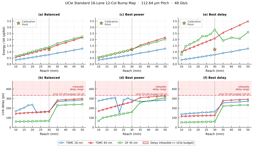
- [Figure 2, Table 1] Figure 2 and Table 1: axis labels and units are inconsistent between power and latency plots; clarify whether values are normalized or absolute.
- [§5] §5: the UCIe case study reports only relative trends; absolute numbers or confidence intervals would strengthen the demonstration.
Simulated Author's Rebuttal
We thank the referee for the constructive feedback on our manuscript. We address the two major comments point-by-point below, indicating planned revisions where appropriate. Our responses focus on clarifying the current manuscript content and strengthening it without overstating the presented evidence.
read point-by-point responses
-
Referee: [Abstract, §4] Abstract and §4 (case study): the central claim that the generated high-level models supply 'enough information to make accurate architectural design decisions' is not supported by any quantitative validation, error metrics, or comparison against silicon measurements or commercial tools; without such evidence the utility assertion remains untested.
Authors: We agree that the manuscript does not provide quantitative error metrics, direct comparisons to silicon measurements, or benchmarks against commercial tools. The case study in §4 illustrates co-optimization workflows using the generated UCIe models across packaging options, but it relies on internal consistency of the PPA estimates rather than external validation data. The abstract claim is framed around enabling exploration for architects lacking packaging expertise, which the framework supports through automated collateral generation. In revision, we will qualify the claim to reflect the demonstrated use case and add an explicit limitations subsection noting the absence of silicon-level validation. revision: partial
-
Referee: [§3] §3 (framework description): the methodology for deriving PPA estimates from packaging parameters is described at a high level but lacks explicit equations, fitting procedures, or parameter sources, making it impossible to assess whether the estimates are independent of the very expertise the framework aims to eliminate.
Authors: The description in §3 is intentionally high-level to focus on the overall framework flow and automation. The PPA estimates combine analytical interconnect models with parameters drawn from published packaging literature and standard foundry design rules. We will revise §3 to include the key equations for delay, power, and area estimation, along with the primary parameter sources and a high-level description of the fitting approach used to calibrate against reference data. This will improve transparency while preserving the framework's goal of reducing required user expertise. revision: yes
Circularity Check
No derivation chain present; framework description only
full rationale
The paper presents an engineering framework for automated generation of chiplet link IP models and collaterals (Verilog, Liberty, LEF, datasheets) along with PPA estimates for 2.5D configurations. The abstract and described claims contain no equations, fitted parameters, predictive derivations, or self-referential steps that could reduce to inputs by construction. No self-citation load-bearing arguments, uniqueness theorems, or ansatzes are invoked. The contribution is the tool and its UCIe case study demonstration, which stands as an independent artifact rather than a closed mathematical loop. This is the expected non-finding for a pure framework paper.
Axiom & Free-Parameter Ledger
Reference graph
Works this paper leans on
-
[1]
Jingwei Cai, Zuotong Wu, Sen Peng, Yuchen Wei, Zhanhong Tan, Guiming Shi, Mingyu Gao, and Kaisheng Ma. 2024. Gemini: Mapping and Architecture Co- exploration for Large-scale DNN Chiplet Accelerators. In2024 IEEE International Symposium on High-Performance Computer Architecture (HPCA). 156–171. doi:10. 1109/HPCA57654.2024.00022
-
[2]
UCIe Consortium. 2024. Universal Chiplet Interconnect Express (UCIe) 2.0 Specification
2024
-
[3]
Behzad Dehlaghi, Nijwm Wary, and Tony Chan Carusone. 2019. Ultra-Short- Reach Interconnects for Die-to-Die Links: Global Bandwidth Demands in Micro- cosm.IEEE Solid-State Circuits Magazine11, 2 (2019), 42–53. doi:10.1109/MSSC. 2019.2910619
-
[4]
Yinxiao Feng and Kaisheng Ma. 2022. Chiplet Actuary: a Quantitative Cost Model and Multi-Chiplet Architecture Exploration. InProceedings of the 59th ACM/IEEE Design Automation Conference(San Francisco, California)(DAC ’22). Association for Computing Machinery, New York, NY, USA, 121–126. doi:10.1145/3489517. 3530428
-
[5]
Yinxiao Feng, Dong Xiang, and Kaisheng Ma. 2023. Heterogeneous Die-to-Die Interfaces: Enabling More Flexible Chiplet Interconnection Systems. InProceed- ings of the 56th Annual IEEE/ACM International Symposium on Microarchitecture (Toronto, ON, Canada)(MICRO ‘23). Association for Computing Machinery, New York, NY, USA, 930–943. doi:10.1145/3613424.3614310
-
[6]
Sandeep Goyal, Ganpat Parulekar, and Shalabh Gupta. 2022. A True Full-Duplex IO (TFD-IO) With Background SI Cancellation for High-Density Interfaces.IEEE Transactions on Very Large Scale Integration (VLSI) Systems30, 5 (2022), 615–624. doi:10.1109/TVLSI.2022.3146326
-
[7]
Alexander Graening, Saptadeep Pal, and Puneet Gupta. 2023. Chiplets: How small is too small?. In2023 60th ACM/IEEE Design Automation Conference (DAC). IEEE, 1–6
2023
-
[9]
Durand Jarrett-Amor, Kunal Yadav, Danny Zhang, Bangda Yang, Sadegh Jalali, and Tony Chan Carusone. 2023. A 32 Gb/s, 0.42 pJ/bit Passive Hybrid Simultaneous Bidirectional Transceiver for Die-to-Die Links. In2023 IEEE International Sympo- sium on Circuits and Systems (ISCAS). 1–5. doi:10.1109/ISCAS46773.2023.10181991
-
[10]
Joohee Kim, Jun So Pak, Jonghyun Cho, Eakhwan Song, Jeonghyeon Cho, Heegon Kim, Taigon Song, Junho Lee, Hyungdong Lee, Kunwoo Park, et al. 2011. High- frequency scalable electrical model and analysis of a through silicon via (TSV). IEEE Transactions on Components, Packaging and Manufacturing Technology1, 2 (2011), 181–195
2011
-
[11]
Kahyun Kim, Jung-Hun Park, Ha-Jung Park, Jia Park, Jihee Kim, and Woo-Seok Choi. 2025. 22.1 A 0.275pJ/b 42Gb/s/pin Clock-Referenced PAM3 Transceiver Tolerant to Supply Noise, Reference Offset and Crosstalk for Chiplets and Short- Reach Memory Interfaces. In2025 IEEE International Solid-State Circuits Confer- ence (ISSCC), Vol. 68. 394–396. doi:10.1109/ISS...
-
[12]
M. Lee, A. Singh, H.M. Torun, J. Kim, S. Lim, M. Swaminathan, and S. Mukhopad- hyay. 2018. Automated Generation of All-Digital I/0 Library Cells for System-in- Package Integration of Multiple Dies. In2018 IEEE 27th Conference on Electrical Performance of Electronic Packaging and Systems (EPEPS). 65–67. doi:10.1109/ EPEPS.2018.8534223
-
[13]
Zixi Li and David Wentzlaff. 2024. LUCIE: A Universal Chiplet-Interposer Design Framework for Plug-and-Play Integration. In2024 57th IEEE/ACM International Symposium on Microarchitecture (MICRO). 423–436. doi:10.1109/MICRO61859. 2024.00039
-
[14]
Susnata Mondal, Sashank Krishnamurthy, Shuhei Yamada, Zhaokai Liu, Junyi Qiu, Soumya Bose, Zuoguo Wu, Gerald Pasdast, James Jaussi, and Mozhgan Mansuri. 2026. A 48Gb/s/lane 1.24Tb/s/mm UCIe-Compliant Die-to-Die Link Over 30mm Standard Package. In2026 IEEE International Solid-State Circuits Conference (ISSCC), Vol. 69. 134–136. doi:10.1109/ISSCC49663.2026.11409120
-
[15]
Lukas Pfromm, Alish Kanani, Harsh Sharma, Parth Solanki, Eric Tervo, Jaehyun Park, Janardhan Doppa, Partha Pratim Pande, and Umit Ogras. 2025. MFIT: Multi-FIdelity Thermal Modeling for 2.5D and 3D Multi-Chiplet Architectures. ACM Trans. Des. Autom. Electron. Syst.31, 1, Article 4 (Nov. 2025), 27 pages. doi:10.1145/3765905
-
[16]
John W. Poulton, John M. Wilson, Walker J. Turner, Brian Zimmer, Xi Chen, Sudhir S. Kudva, Sanquan Song, Stephen G. Tell, Nikola Nedovic, Wenxu Zhao, Sunil R. Sudhakaran, C. Thomas Gray, and William J. Dally. 2019. A 1.17-pJ/b, 25- Gb/s/pin Ground-Referenced Single-Ended Serial Link for Off- and On-Package Communication Using a Process- and Temperature-Ad...
-
[17]
Shibkov, Antonio La Manna, Geert van der Plas, and Eric Beyne
Mirko Scholz, Geert Hellings, Shih-Hung Chen, Dimitri Linten, Mikael Detalle, Cesar Roda Neve, A. Shibkov, Antonio La Manna, Geert van der Plas, and Eric Beyne. 2015. ESD protection design in active-lite interposer for 2.5 and 3D systems-in-package. In2015 37th Electrical Overstress/Electrostatic Discharge Sym- posium (EOS/ESD). 1–10. doi:10.1109/EOSESD.2...
-
[18]
Zhanhong Tan, Hongyu Cai, Runpei Dong, and Kaisheng Ma. 2021. NN-Baton: DNN Workload Orchestration and Chiplet Granularity Exploration for Multi- chip Accelerators. In2021 ACM/IEEE 48th Annual International Symposium on Computer Architecture (ISCA). 1013–1026. doi:10.1109/ISCA52012.2021.00083
-
[19]
Rao R Tummala et al. 2001. Fundamentals of microsystems packaging. (2001)
2001
-
[20]
Zhenyu Wang, Pragnya Sudershan Nalla, Jingbo Sun, A Alper Goksoy, Sumit K Mandal, Jae-sun Seo, Vidya A Chhabria, Jeff Zhang, Chaitali Chakrabarti, Umit Y Ogras, et al. 2025. HISIM: Analytical Performance Modeling and Design Space Exploration of 2.5 D/3D Integration for AI Computing.IEEE Transactions on Computer-Aided Design of Integrated Circuits and Syst...
2025
-
[21]
Wright, R
S.L. Wright, R. Polastre, H. Gan, L.P. Buchwalter, R. Horton, P.S. Andry, E. Sprogis, C. Patel, C. Tsang, J. Knickerbocker, J.R. Lloyd, A. Sharma, and M.S. Sri-Jayantha
-
[22]
In56th Electronic Components and Technology Conference 2006
Characterization of micro-bump C4 interconnects for Si-carrier SOP appli- cations. In56th Electronic Components and Technology Conference 2006. 8 pp.–. doi:10.1109/ECTC.2006.1645716
-
[23]
Yang Zhang, Xuchen Zhang, and Muhannad S Bakir. 2018. Benchmarking digital die-to-die channels in 2.5-D and 3-D heterogeneous integration platforms.IEEE Transactions on Electron Devices65, 12 (2018), 5460–5467
2018
-
[24]
Minghao Zhou, Li Li, Fengze Hou, Guoqiang He, and Jiaqi Fan. 2022. Thermal Modeling of a Chiplet-Based Packaging With a 2.5-D Through-Silicon Via Inter- poser.IEEE Transactions on Components, Packaging and Manufacturing Technology 12, 6 (2022), 956–963. doi:10.1109/TCPMT.2022.3174608
discussion (0)
Sign in with ORCID, Apple, or X to comment. Anyone can read and Pith papers without signing in.