Pith. sign in

REVIEW 2 major objections 5 minor 5 references

Small but Tubby: A Magnetic Loop Antenna Made from 100 mm Copper Tubing

T0 review · 2 major / 5 minor · reviewed 2026-07-14 · grok-4.5

Pith's one-line read Indoor magnetic-loop losses come mostly from near-field coupling to the building, not from the antenna itself.

desk verdict Solid instrumentation paper: the thermal budget really does show the building, not the 100 mm loop, eats most of the indoor loss power. read the letter →

arxiv 2607.10828 v1 pith:SUSYQGF4 submitted 2026-07-12 physics.ins-det

classification physics.ins-det
keywords magneticloopantennasmalltransmittingvacuumcapacitorefficiencygammamatchindoornear-fieldcouplingthermalmeasurement
verification ladder T0 review T1 audit T2 compute T3 formal

The pith

A machine-rendered reading of the paper's core claim, the machinery that carries it, and where it could break.

The reading

This paper presents the model, construction, and measurements of a small transmitting magnetic loop built from unusually thick 100 mm copper tubing with vacuum capacitors and servo-driven automatic tuning from 1.8 to 31 MHz. The large conductor surface and wide transitions were chosen to keep the antenna’s own resistive losses as low as possible. When the same loop is used indoors, measured total resistance rises sharply; temperature-rise tests show the copper and capacitors barely warm while tens of watts of the non-radiated power disappear into the surroundings. The authors conclude that indoor losses are dominated by near-field coupling into walls, floors, roof moisture and other nearby materials rather than by the antenna components. The result matters for anyone forced to radiate HF indoors: once the environment absorbs most of the power, further polishing of the loop itself yields little extra radiated power.

What carries the argument

Total loop resistance R_T extracted from measured SWR-2.62 bandwidth, then partitioned with free-space radiation resistance R_R (King formula) so that efficiency η = R_R/R_T and loop current I = √(P/R_T) can be estimated; thermal imaging and free-space H-field comparisons then locate the dominant loss term as environmental near-field absorption R_E.

What would settle it

Deliver a known power (for example 80 W) into the indoor loop for a fixed interval while recording calibrated temperature rise of the copper tubing and capacitors; if the antenna’s own heating accounts for most of the non-radiated power budget rather than only a few watts, the claim that the environment absorbs the bulk is false.

Watch

Extended reading notes

Core claim

For a carefully minimized magnetic loop operated indoors, the bulk of the dissipated power is absorbed by the surrounding building through near-field coupling, not by the antenna conductors or capacitors. Outdoor loss resistance can fall to roughly 0.014 Ω at 14 MHz, while the same antenna indoors shows hundreds of milliohms of additional loss; after 100 W transmission the antenna itself heats by less than a few watts of the calculated loss budget.

Load-bearing premise

The free-space radiation-resistance formula still correctly tells how much of the measured total resistance is truly radiated once the loop sits indoors among lossy objects.

Editorial extensions

If this is right

  • Once environmental near-field absorption dominates, further reduction of conductor or capacitor losses barely improves indoor radiated power.
  • A simpler thinner-tube or air-capacitor loop can perform nearly as well indoors as an elaborately low-loss design.
  • Increasing loop diameter does not reliably raise indoor radiated power, because environmental loss resistance scales with the near-field pattern in a similar way.
  • Safety estimates that ignore environmental damping will overestimate loop current and near-field H-field indoors.
  • Direct H-field probing remains a practical check on actual loop current when bandwidth-derived current is uncertain.

Reading between the lines

Editorial extensions of the paper, not claims the author makes directly.

  • Indoor HF operators may gain more by moving the loop away from lossy materials (wet green roofs, aluminium-coated underfloor pipes) than by investing in exotic low-loss capacitors.
  • The same near-field absorption mechanism is likely to limit other electrically small indoor antennas, not only magnetic loops.
  • Routing control wiring inside the loop conductor, so the tuning motor needs no high-voltage insulation, is a reusable mechanical idea for other high-Q indoor radiators.
Share X Bluesky LinkedIn Reddit HN

Signed reviews

No signed human review yet.

Editorial analysis

A structured set of objections, weighed in public.

Desk editor's note, referee report, and a circularity audit.

Referee Report

2 major / 5 minor

Summary. The manuscript presents the design, electrical model, construction details, and extensive measurements of a small transmitting magnetic-loop antenna fabricated from 100 mm copper tubing, covering 1.8–31 MHz with servo-driven automatic frequency, matching, and azimuth control. A novel internal routing of control wiring places the frequency-tuning servo inside the conductor (field-free region) without high-voltage insulation. The central experimental claim is that, for indoor operation, the dominant contribution to the measured total resistance RT is environmental near-field absorption RE rather than conductor or capacitor losses; this is supported by outdoor-versus-indoor bandwidth comparisons, height and moisture dependence, and a calibrated thermal budget at 28 MHz showing antenna self-heating well below 5 W of an ~52 W non-radiated power share. Conducted H-field probe data are shown to agree with free-space magnetic-dipole predictions that use loop current inferred from measured bandwidth and delivered power.

Significance. If the thermal and bandwidth results hold, the work supplies a carefully documented, reproducible demonstration that indoor magnetic-loop performance is limited by building coupling rather than by the antenna’s own ohmic losses—an important practical distinction for restricted-site HF operation. Strengths include the explicit SWR-2.62 unloaded-Q derivation (Appendix 7.1), the independent 5 W LED thermal calibration, the multi-band outdoor/indoor data set, and the authors’ own caveats on free-space RR and indoor efficiency interpretation (§3.13–3.15). The construction record (large-area transitions, vacuum-capacitor details, gamma-match geometry) and open discussion of failed capacitor experiments add archival value for the instrumentation community.

major comments (2)
  1. [Abstract; §3.3; Figure 74] The abstract and §3.3 report numerical efficiencies η = RR/RT derived from the free-space King formula (Eq. 9) applied to the rectangular loop’s equivalent circular diameter. While the thermal evidence that antenna components dissipate ≪ RE is independent of this partition (§3.12), the efficiency numbers themselves remain free-space equivalents. A short, consistent qualification in the abstract and in the caption of Figure 74 would prevent over-reading of the indoor η values, especially given the authors’ own discussion in §3.15 that RR may be underestimated at higher frequencies.
  2. [§3.7; Eq. (5)] Loop current I_main = √(P/RT) (Eq. 5) and the subsequent free-space H-field comparison (§3.7) both inherit the measured RT that already includes RE. The good numerical agreement with the retarded-dipole formula is therefore expected once the reduced current is inserted; it does not independently confirm that the free-space RR component actually reaches the far field. The manuscript already notes limited building attenuation of H (§3.7), but a clearer statement that the H-probe test validates the current estimate rather than the radiated-power fraction would tighten the logic.
minor comments (5)
  1. [§2.6; Eq. (1), Eq. (9)] The rectangular geometry (0.95 m × 0.85 m) is replaced by an equivalent circular diameter of 1.014 m for both L (Eq. 1) and RR (Eq. 9). A one-sentence justification or a brief comparison with a rectangular-loop inductance formula would reassure readers that the approximation error is negligible relative to the large environmental uncertainties.
  2. [§3.3; Figure 74] Figure 74 and the accompanying table of derived resistances would benefit from explicit listing of the feeder-loss correction factors k applied to each band (already tabulated in Figure 83) so that the reader can reconstruct RT without referring to the appendix.
  3. [§1.2.2] In §1.2.2 the gamma-match is described as “asymmetric” yet “minimal for high-Q”; a quantitative estimate of the residual common-mode voltage or a reference to the choke measurements in §3.10 would make the claim more precise.
  4. [§3.12] Several thermal images (Figures 85–87) rely on painter’s-tape emissivity ≈ 1; a brief note that the shiny copper surfaces were not used for quantitative ΔT would avoid misinterpretation by readers unfamiliar with IR thermography.
  5. [throughout] Typographical: “efÏciency” appears repeatedly (encoding artifact); replace with “efficiency”. Also “positron.ch” URL in the header is fine for the preprint but should be removed or replaced by a permanent DOI for journal production.

Circularity Check

1 steps flagged · score 1.0 of 10

No load-bearing circularity: RT from bandwidth, RR from external King free-space formula, and thermal bounds on antenna self-heating are independent; I→H comparison is standard consistency check, not a forced prediction.

  1. fitted input called prediction [Abstract; §1.5 Eqs. 11–12; §3.7 (H-field comparison)]
    "The conducted H-field measurements demonstrate good agreement between the measured H-field and the theoretical free-space H-field calculated from the antenna geometry and an estimated loop current. The loop current was estimated from the measured antenna bandwidth and the applied transmit power."

    I_main is obtained from measured RT (via bandwidth) and applied P, then plugged into the free-space dipole H formula and compared to probe readings. This is a consistency check, not a free prediction of a new observable; agreement partly reconfirms the same current estimate already used to form the power budget. It is standard practice and not load-bearing for the environmental-loss claim (which is carried by thermal imaging and outdoor/indoor RT contrast), hence only a minor flag.

full rationale

The paper’s derivation chain is measurement-plus-standard-circuit theory, not a closed self-definitional loop. Unloaded Q0 and total resistance RT are obtained from measured SWR-2.62 bandwidth (Eqs. 3–4); radiation resistance RR is taken from the external free-space King formula (Eq. 9); efficiency η = RR/RT and loop current I = √(P/RT) then follow by definition of those quantities. The central indoor-loss claim (Abstract, §3.8, §3.12) rests on (i) outdoor vs indoor RT contrast (outdoor R_loss ≈ 0.014 Ω vs indoor ≈ 0.607 Ω) and (ii) a direct thermal experiment: 10 min at ~80 W delivered produces no measurable antenna temperature rise (<0.3 °C) while a 5 W LED heater inside the tubing yields a clear 2.1 °C rise, bounding antenna dissipation well below 5 W of the non-radiated budget. That thermal bound does not depend on the King RR partition. The only mild self-reference is reuse of the bandwidth-derived I_main to compute a free-space H-field for comparison with probe data (§1.5, §3.7)—standard validation practice, not a fit renamed as prediction. No self-citation uniqueness theorems, no ansatz smuggled via prior author work, and no renaming of a known empirical pattern as a first-principles result. Score 1 only for the minor I→H reuse; the paper is otherwise self-contained against external benchmarks.

Assumptions & free parameters 2 free parameters · 5 assumptions · 0 invented entities

The work is experimental engineering on top of textbook small-loop theory. Load-bearing content is measured R_T, thermal bounds, and H-probe data. Free parameters are only measurement corrections (cable loss, delivered power). Axioms are standard electromagnetics and the modeling choice that environmental absorption appears as a lumped R_E. No new particles, forces, or ad-hoc physical entities are introduced.

free parameters (2)
  • feeder one-way attenuation L used for bandwidth correction factor k = band-dependent; e.g. factors listed in Fig. 83
    Cable losses measured after the fact and used to correct VNA-reported SWR-2.62 bandwidths (§3.11, Eq. 27 in §7.3); correction multiplies into every R_T and efficiency number.
  • delivered antenna power P after cable/connector loss = ~80–94 W from 100 W TX
    Transmitter display (100 W) reduced by estimated cable loss (~1 dB → 80–94 W depending on section) before I_main = √(P/R_T) and power budgets (§3.7, §3.12).
assumptions (5)
  • domain assumption Single-turn loop inductance L ≈ μ0 D/2 (ln(8D/d) − 2) under strong skin effect (§1.1 Eq. 1)
    Standard high-frequency tube-loop formula; validated roughly by resonance measurements but not re-derived.
  • domain assumption King radiation resistance formula for circular loops with uniform current, including large-loop correction (§1.3 Eqs. 8–9)
    Used to compute R_R and thus efficiency η = R_R/R_T for all bands; accuracy at higher HF is questioned by the authors themselves (§3.15).
  • standard math Unloaded Q0 = f0 / B_SWR2.62 and R_T = X_L / Q0 from matched SWR=2.62 bandwidth (Appendix 7.1)
    Derived from |Γ| at Z = 50(1±j); standard resonator result applied throughout §3.
  • domain assumption Environmental near-field absorption can be represented as a lumped series resistance R_E in the loop circuit (§1.1, §1.7)
    Modeling choice that lets indoor bandwidth increase be read as extra loss resistance; supported by dummy-load analogy figures but is an effective-circuit abstraction.
  • domain assumption Retarded magnetic-dipole H-field formula for free space (§1.5 Eq. 12) applied to equivalent-diameter circular approximation of the rectangular loop
    Used as the theoretical baseline for indoor H-probe comparisons in §3.7.

how reviews work

0 comments
Cite this review

Pith. "Pith review of Small but Tubby: A Magnetic Loop Antenna Made from 100 mm Copper Tubing." pith.science (2026). https://pith.science/paper/SUSYQGF4

@misc{pith2026260710828,
  author       = {Pith},
  title        = {Pith review of: Small but Tubby: A Magnetic Loop Antenna Made from 100 mm Copper Tubing},
  year         = {2026},
  howpublished = {\url{https://pith.science/paper/SUSYQGF4}},
  note         = {Machine review of arXiv:2607.10828}
}
read the original abstract

This paper presents the electrical model, key equations, and practical construction of a small transmitting magnetic loop antenna built from unusually large 100 mm diameter copper tubing. The large conductor surface area and wide-area transitions to the vacuum capacitors were designed to minimize resistive losses. The frequency range from 1.8 MHz to 31 MHz is unusually wide. Frequency, impedance matching, and azimuth are all adjusted automatically by servo motors. A novel feature is the routing of the control wiring inside the loop conductor, allowing the motor to be mounted without electrical insulation from the loop conductor. Indoor losses originate predominantly from near-field coupling to the environment rather than from the antenna itself. Temperature-rise measurements confirm that the bulk of the dissipated power is absorbed by the environment, not by the antenna components. The conducted H-field measurements demonstrate good agreement between the measured H-field and the theoretical free-space H-field calculated from the antenna geometry and an estimated loop current. The loop current was estimated from the measured antenna bandwidth and the applied transmit power. The antenna was developed for indoor operation where outdoor installation is not possible.

Figures

Figures reproduced from arXiv: 2607.10828 by the authors.

Figure 1
Figure 1. Magnetic loop antenna: main loop and capacitor. [PITH_FULL_IMAGE:figures/full_fig_p003_1.png] view at source ↗
Figure 3
Figure 3. Inductance of a ring-shaped tube. For a single-turn circular loop with mean diameter 𝐷 and conductor diameter 𝑑, the approximate inductance is given by: 𝐿 = 𝜇0 ⋅ 𝐷 2 (ln(8𝐷 𝑑 ) − 2) (1) where 𝜇0 = 4𝜋 ⋅ 10−7 𝐻 𝑚. This approximation assumes a pronounced skin effect where the current flows only on the conductor’s surface (e.g., in high-frequency applications or thin-walled tubing). The resonance frequency of the tuned … view at source ↗
Figure 4
Figure 4. The resonant circuit is damped; this is modeled by inserting a resistance ( [PITH_FULL_IMAGE:figures/full_fig_p004_4.png] view at source ↗
Figures from the paper (87 more)
Figure 7
Figure 7. Figure 7: The transmitter, with a 50 Ω internal resistance, delivers the RF power [PITH_FULL_IMAGE:figures/full_fig_p004_7.png]
Figure 8
Figure 8. Figure 8: Coupling loop overview: coaxial cable from TX to antenna, with the lower part of the main [PITH_FULL_IMAGE:figures/full_fig_p006_8.png]
Figure 9
Figure 9. Figure 9: For simplification, the source TX is moved all the way to the top. This simplification is fu [PITH_FULL_IMAGE:figures/full_fig_p006_9.png]
Figure 10
Figure 10. Figure 10: Coupling-loop current flow: Moving the source TX to the top allows us to draw a functional [PITH_FULL_IMAGE:figures/full_fig_p006_10.png]
Figure 11
Figure 11. Figure 11: The coupling ratio (equivalent turns ratio) between the coupling loop and the main loop d [PITH_FULL_IMAGE:figures/full_fig_p007_11.png]
Figure 12
Figure 12. Figure 12: The outer conductor of the coaxial cable is galvanically connected to the main loop at th [PITH_FULL_IMAGE:figures/full_fig_p008_12.png]
Figure 13
Figure 13. Figure 13: The gamma match is rotatably mounted (red: rotation axis). Position with minimal coupling [PITH_FULL_IMAGE:figures/full_fig_p008_13.png]
Figure 14
Figure 14. Figure 14: Coordinate system used for the figures in this document. Main loop in red. [PITH_FULL_IMAGE:figures/full_fig_p010_14.png]
Figure 15
Figure 15. Figure 15: Simulated magnetic field strength (H) around the loop antenna. [PITH_FULL_IMAGE:figures/full_fig_p011_15.png]
Figure 16
Figure 16. Figure 16: Simulated magnetic field strength (H), wide-view map showing the transition toward the far [PITH_FULL_IMAGE:figures/full_fig_p012_16.png]
Figure 17
Figure 17. Figure 17: Normalized linear far-field radiation pattern of a loop antenna. [PITH_FULL_IMAGE:figures/full_fig_p012_17.png]
Figure 18
Figure 18. Figure 18: A magnetic loop is shown with its loss resistances. The antenna couples to a dummy load ( [PITH_FULL_IMAGE:figures/full_fig_p013_18.png]
Figure 19
Figure 19. Figure 19: The dummy load has been replaced by a wall. The wall absorbs energy from the antenna’s ne [PITH_FULL_IMAGE:figures/full_fig_p013_19.png]
Figure 20
Figure 20. Figure 20: Now the wall is removed and the antenna stands in free space. The gamma match has been re [PITH_FULL_IMAGE:figures/full_fig_p014_20.png]
Figure 21
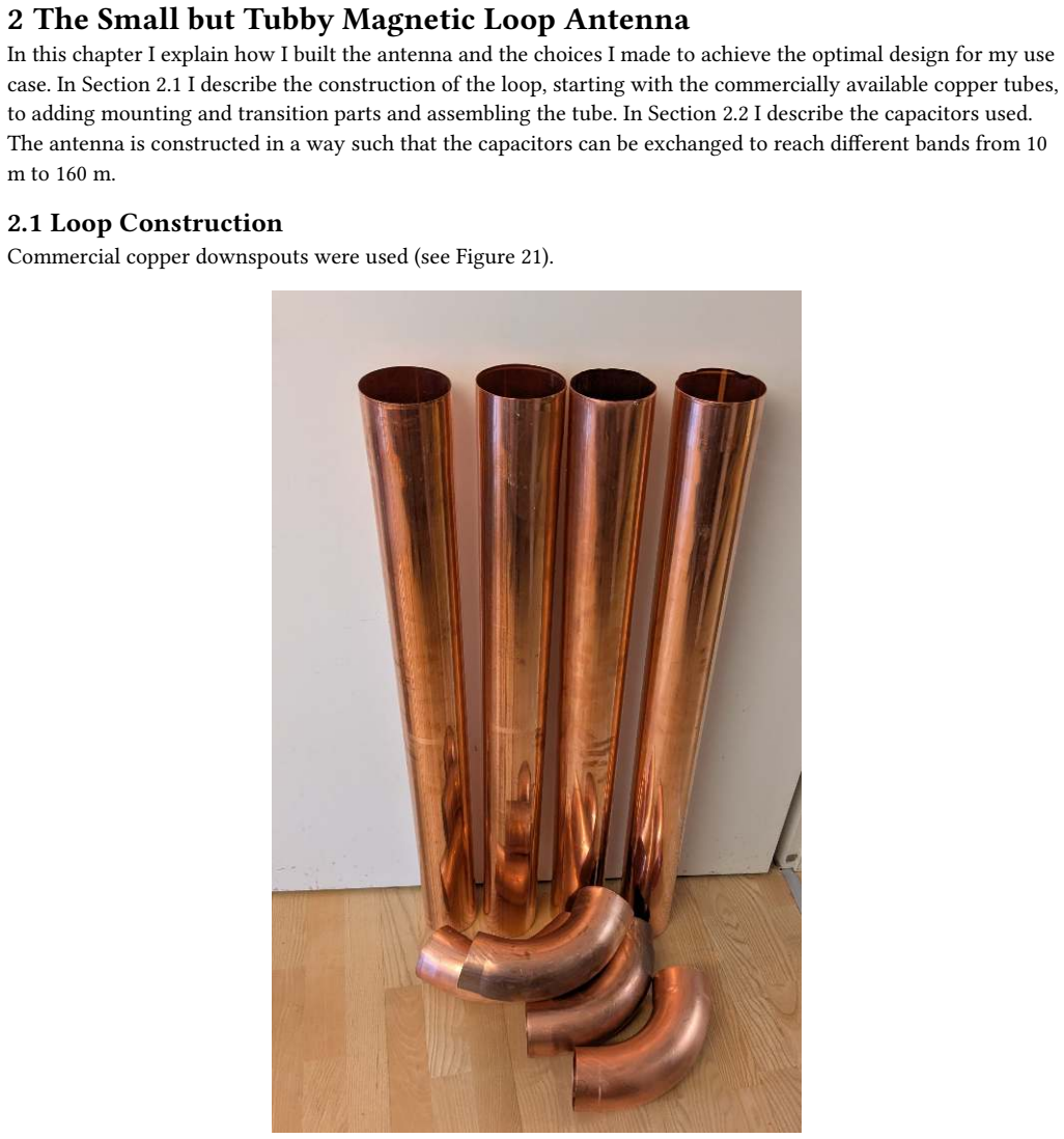
Figure 21. Figure 21: Commercially available copper downspouts with 100 mm diameter. [PITH_FULL_IMAGE:figures/full_fig_p015_21.png]
Figure 22
Figure 22. Figure 22: Copper parts for mounting the coupling loop. [PITH_FULL_IMAGE:figures/full_fig_p016_22.png]
Figure 23
Figure 23. Figure 23: Transitions from pipe to capacitors with glued-on cutting patterns. [PITH_FULL_IMAGE:figures/full_fig_p016_23.png]
Figure 24
Figure 24. Figure 24: Annealed and bent transitions. The surface is still black from copper oxide. [PITH_FULL_IMAGE:figures/full_fig_p016_24.png]
Figure 25
Figure 25. Figure 25: Clamping the copper parts securely before soldering. [PITH_FULL_IMAGE:figures/full_fig_p017_25.png]
Figure 26
Figure 26. Figure 26: Soldering joint after removing flux residues. [PITH_FULL_IMAGE:figures/full_fig_p017_26.png]
Figure 27
Figure 27. Figure 27: Removing excess solder with a milling cutter. [PITH_FULL_IMAGE:figures/full_fig_p018_27.png]
Figure 28
Figure 28. Figure 28: Surface after milling and sanding. The current flows through the solder for only a very sho [PITH_FULL_IMAGE:figures/full_fig_p018_28.png]
Figure 29
Figure 29. Figure 29: Finished soldered loop [PITH_FULL_IMAGE:figures/full_fig_p019_29.png]
Figure 30
Figure 30. Figure 30: Loop before final cleaning with steel wool. [PITH_FULL_IMAGE:figures/full_fig_p019_30.png]
Figure 31
Figure 31. Figure 31: Loop finished and varnished [PITH_FULL_IMAGE:figures/full_fig_p020_31.png]
Figure 32
Figure 32. Figure 32: Transition to the variable capacitor. The flattened pipe section is 100 mm wide and is scr [PITH_FULL_IMAGE:figures/full_fig_p020_32.png]
Figure 33
Figure 33. Figure 33: Configuration for 10 m to 40 m: only the variable capacitor is connected. Capacitor A is m [PITH_FULL_IMAGE:figures/full_fig_p020_33.png]
Figure 34
Figure 34. Figure 34: Configuration for 60 m: capacitor A 500 pF is electrically connected. The side screws pres [PITH_FULL_IMAGE:figures/full_fig_p021_34.png]
Figure 35
Figure 35. Figure 35: Configuration for 80 m: additional capacitor B 500 pF is installed. [PITH_FULL_IMAGE:figures/full_fig_p021_35.png]
Figure 36
Figure 36. Figure 36: Left: variable vacuum capacitor KP1-4 10–500 pF. Right: when the capacitor is set to minim [PITH_FULL_IMAGE:figures/full_fig_p021_36.png]
Figure 37
Figure 37. Figure 37: Left: the author and the capacitor wrapped in cardboard as implosion protection. I had no [PITH_FULL_IMAGE:figures/full_fig_p022_37.png]
Figure 38
Figure 38. Figure 38: View of the concentric interleaving vanes. [PITH_FULL_IMAGE:figures/full_fig_p022_38.png]
Figure 39
Figure 39. Figure 39: Turning the shaft clockwise retracts one set of vanes, reducing the capacitance. An intern [PITH_FULL_IMAGE:figures/full_fig_p022_39.png]
Figure 40
Figure 40. Figure 40: Left: vanes fully separated, 10 pF. Right: vanes fully interleaved, 500 pF. The spring tha [PITH_FULL_IMAGE:figures/full_fig_p023_40.png]
Figure 41
Figure 41. Figure 41: Capacitance characteristics versus turns of the axis. Reproduced with kind permission of [PITH_FULL_IMAGE:figures/full_fig_p023_41.png]
Figure 42
Figure 42. Figure 42: Cross-sectional detail showing the movable copper bellows, which not only provides the va [PITH_FULL_IMAGE:figures/full_fig_p023_42.png]
Figure 43
Figure 43. Figure 43: The transition from glass to copper was made by fusing glass and copper together. [PITH_FULL_IMAGE:figures/full_fig_p024_43.png]
Figure 44
Figure 44. Figure 44: Left: view of a fracture point; when looking through the glass from outside, a yellow colo [PITH_FULL_IMAGE:figures/full_fig_p024_44.png]
Figure 45
Figure 45. Figure 45: On this capacitor specimen, arcing marks are clearly visible. [PITH_FULL_IMAGE:figures/full_fig_p024_45.png]
Figure 46
Figure 46. Figure 46: Left: close-up of an arcing pit, finely recessed and barely visible in the photograph. Righ [PITH_FULL_IMAGE:figures/full_fig_p025_46.png]
Figure 47
Figure 47. Figure 47: The arcing marks appear only at the outermost gap. The outermost vane is slightly bent ou [PITH_FULL_IMAGE:figures/full_fig_p025_47.png]
Figure 48
Figure 48. Figure 48: Clamps manufactured from 12 mm OF copper as a transition from the capacitor ends to the c [PITH_FULL_IMAGE:figures/full_fig_p026_48.png]
Figure 49
Figure 49. Figure 49: Capacitor assembly. The servo_f is located inside the copper tube and is therefore in a fi [PITH_FULL_IMAGE:figures/full_fig_p026_49.png]
Figure 50
Figure 50. Figure 50: Jennings JCS-500-10S vacuum capacitor. Two of these are used. [PITH_FULL_IMAGE:figures/full_fig_p027_50.png]
Figure 51
Figure 51. Figure 51: Turned sleeves made of OF copper serving as transition from vacuum capacitor to copper tu [PITH_FULL_IMAGE:figures/full_fig_p027_51.png]
Figure 52
Figure 52. Figure 52: Markings: type designation ФГТ-И (FGT-I series, PTFE dielectric), 4700 пФ ±10% (4700 pF ± [PITH_FULL_IMAGE:figures/full_fig_p028_52.png]
Figure 53
Figure 53. Figure 53: Left: circuit boards as delivered by the manufacturer. Center: soldering the plates with a [PITH_FULL_IMAGE:figures/full_fig_p029_53.png]
Figure 54
Figure 54. Figure 54: Left: spacers 3D-printed from PETG; the spacers prevent the plates from touching. Center: [PITH_FULL_IMAGE:figures/full_fig_p029_54.png]
Figure 55
Figure 55. Figure 55: To corroborate the suspicion of losses in the spacers, two special spacers were fabricate [PITH_FULL_IMAGE:figures/full_fig_p029_55.png]
Figure 56
Figure 56. Figure 56: Left: new spacers with less material, made from COC (Cyclo Olefin Copolymer). COC should ex [PITH_FULL_IMAGE:figures/full_fig_p030_56.png]
Figure 57
Figure 57. Figure 57: Left: a single capacitor with 2800 pF. Right: capacitors loosely connected with metal shee [PITH_FULL_IMAGE:figures/full_fig_p031_57.png]
Figure 58
Figure 58. Figure 58: Left: assembled 4200 pF capacitor, weighing 2.3 kg. The capacitors are firmly bolted togeth [PITH_FULL_IMAGE:figures/full_fig_p031_58.png]
Figure 59
Figure 59. Figure 59: Left: Smith chart — the trace has an unusual shape; it should be circular. Center: SWR ver [PITH_FULL_IMAGE:figures/full_fig_p031_59.png]
Figure 60
Figure 60. Figure 60: In stark contrast to the unusual behavior shown above, here is a measurement at 14 MHz fo [PITH_FULL_IMAGE:figures/full_fig_p032_60.png]
Figure 61
Figure 61. Figure 61: Left: after 10 minutes of transmitting at 100 W, the Comet capacitors heated up by 3.7 °C, [PITH_FULL_IMAGE:figures/full_fig_p032_61.png]
Figure 62
Figure 62. Figure 62: Gamma match constructed from 12 mm diameter copper tubing with a total length of 0.7 m. [PITH_FULL_IMAGE:figures/full_fig_p033_62.png]
Figure 63
Figure 63. Figure 63: Left: small coupling; right: large coupling. The servo_z automatically adjusts the couplin [PITH_FULL_IMAGE:figures/full_fig_p033_63.png]
Figure 64
Figure 64. Figure 64: Pivot joint in the center of the loop with galvanic connection to the main loop. [PITH_FULL_IMAGE:figures/full_fig_p033_64.png]
Figure 65
Figure 65. Figure 65: Cable routing and placement of the electronic components are exactly in the symmetry plan [PITH_FULL_IMAGE:figures/full_fig_p034_65.png]
Figure 66
Figure 66. Figure 66: Below the antenna, the servo_h controls the azimuth. The servo axis is centered directly [PITH_FULL_IMAGE:figures/full_fig_p034_66.png]
Figure 67
Figure 67. Figure 67: Schematic of the antenna system including tuning servos and magnetometer. [PITH_FULL_IMAGE:figures/full_fig_p035_67.png]
Figure 68
Figure 68. Figure 68: Example of a conventional design. The tuning capacitor is mounted vertically at the top o [PITH_FULL_IMAGE:figures/full_fig_p036_68.png]
Figure 69
Figure 69. Figure 69: Left: the antenna presented in this paper. Center: the control cables (red) run through th [PITH_FULL_IMAGE:figures/full_fig_p036_69.png]
Figure 70
Figure 70. Figure 70: Calculated frequency ranges for different capacitor configurations. [PITH_FULL_IMAGE:figures/full_fig_p037_70.png]
Figure 71
Figure 71. Figure 71: Cross-sectional house model used for the measurement setup. [PITH_FULL_IMAGE:figures/full_fig_p038_71.png]
Figure 72
Figure 72. Figure 72: Antenna on the ground and at maximum height. [PITH_FULL_IMAGE:figures/full_fig_p038_72.png]
Figure 73
Figure 73. Figure 73: Indoor antenna setup: left, indoor measurement geometry; right, installation photo. [PITH_FULL_IMAGE:figures/full_fig_p039_73.png]
Figure 74
Figure 74. Figure 74: Measured bandwidths. Derived resistances and estimated antenna efÏciency. [PITH_FULL_IMAGE:figures/full_fig_p039_74.png]
Figure 75
Figure 75. Figure 75: Estimated loss resistance 𝑅loss as a function of height above ground for two frequencies for the 20 m band (14 MHz). Findings: • The loss resistance decreases continuously with increasing height as expected. With even greater distance from surrounding objects, the los…
Figure 76
Figure 76. Figure 76: Clip-on ferrite cores attached to the exposed underfloor heating pipes on the upper floor. [PITH_FULL_IMAGE:figures/full_fig_p041_76.png]
Figure 77
Figure 77. Figure 77: Left: simple self-made H-field probe. The induced voltage is measured with an inexpensive p [PITH_FULL_IMAGE:figures/full_fig_p042_77.png]
Figure 78
Figure 78. Figure 78: Left column, top: measurement points with calculated and measured H-field; the factor shows [PITH_FULL_IMAGE:figures/full_fig_p043_78.png]
Figure 79
Figure 79. Figure 79: Left: impression of the top timber-frame story; at this stage the room was still open, and [PITH_FULL_IMAGE:figures/full_fig_p044_79.png]
Figure 80
Figure 80. Figure 80: Comparison of two magnetic loops with diameters of 1.0 m (a) and 0.5 m (b). Both loops pr [PITH_FULL_IMAGE:figures/full_fig_p045_80.png]
Figure 81
Figure 81. Figure 81: Overlay of the field lines of both loops from Figure 80. The gray hatched region indicates [PITH_FULL_IMAGE:figures/full_fig_p046_81.png]
Figure 82
Figure 82. Figure 82: Common-mode choke assemblies used on the coax feed and servo control line. Right: example [PITH_FULL_IMAGE:figures/full_fig_p047_82.png]
Figure 83
Figure 83. Figure 83: Measured indoor and outdoor bandwidths at the VNA, measured cable losses and the resultin [PITH_FULL_IMAGE:figures/full_fig_p048_83.png]
Figure 84
Figure 84. Figure 84: Left: the RG8U feed cable warmed by 1.1°C and the 17-turn choke by 8.2°C, consistent with [PITH_FULL_IMAGE:figures/full_fig_p049_84.png]
Figure 85
Figure 85. Figure 85: The antenna itself shows no visible heating (below about 0.3°C at taped measurement point [PITH_FULL_IMAGE:figures/full_fig_p049_85.png]
Figure 86
Figure 86. Figure 86: No antenna parts show measurable heating; temperatures are read on painter’s tape (emissi [PITH_FULL_IMAGE:figures/full_fig_p050_86.png]
Figure 87
Figure 87. Figure 87: Left: view into the left tube section. The LEDs are lit and heat the tube. Right: thermal i [PITH_FULL_IMAGE:figures/full_fig_p050_87.png]
Figure 88
Figure 88. Figure 88: Summary of the heating experiment: power budget for 100 W transmit power. [PITH_FULL_IMAGE:figures/full_fig_p051_88.png]
Figure 89
Figure 89. Figure 89: Not everything worked on the first attempt — it was a tough journey with many setbacks. Bu [PITH_FULL_IMAGE:figures/full_fig_p053_89.png]
Figure 90
Figure 90. Figure 90: Many things ended up in the bin — or, in the case of this magnetic loop, in the scrap cop [PITH_FULL_IMAGE:figures/full_fig_p053_90.png]
Figure 91
Figure 91. Figure 91: Map of digital-mode contacts made during the first months of operation. Source: GridTracke [PITH_FULL_IMAGE:figures/full_fig_p053_91.png]
Figure 92
Figure 92. Figure 92: Left: Peter Märki with his brother Hans Märki; right: Peter Schär measuring antenna height [PITH_FULL_IMAGE:figures/full_fig_p054_92.png]
Figure 93
Figure 93. Figure 93: The authors: left, Markus Niese with Peter Märki; right, Loopie with Peter Märki. [PITH_FULL_IMAGE:figures/full_fig_p054_93.png]

Discussion (0). Continue with ORCID to comment.

Reference graph

Works this paper leans on

5 extracted references · 1 canonical work pages

  1. [1]

    and [3]. This section focuses on two similar methods, both are mechanically and electrically elegant solutions: First, I will discuss the shielded coaxial coupling loop, a small complete coupling loop that is magnetically coupled to the main loop, then I will discuss the gamma match feed system, which only has half a loop in addition to the main loop. The...

  2. [2]

    Kontakt Chemie PLASTIK 70

    Examples of H-field measurements can be found in Section 3.7. 1.6 Far-Field Radiation Pattern The following figure shows the normalized linear far-field radiation characteristic. Figure 17: Normalized linear far-field radiation pattern of a loop antenna. In the far-field region, the magnetic loop antenna exhibits a figure-eight radiation pattern, with max...

  3. [3]

    During transmission, the behavior was puzzling: the FT-991A showed an SWR on the order of 2.1 and above and reduced the transmit power from 100 to 60 W to protect its output stage

    This is discussed further there. During transmission, the behavior was puzzling: the FT-991A showed an SWR on the order of 2.1 and above and reduced the transmit power from 100 to 60 W to protect its output stage. The voltage across the capacitor is less than 900 Vrms, which should still be acceptable at a 1 mm plate gap. Heating and detuning due to losse...

  4. [4]

    URN: urn:nbn:de:hbz:465-20220322-135255-6

    DOI: 10.17185/duepublico/75498. URN: urn:nbn:de:hbz:465-20220322-135255-6. •

  5. [5]

    Quality factor

    Credits: Green person: José Pedro, CC BY‑NC‑SA 4.0, https://www.printables.com/model/1389190-super-collection-of-miniature-people-194-figures. 7 Appendix 7.1 Measurement at SWR 2.62 The bandwidth of the unloaded parallel RLC resonant circuit is generally defined by the frequencies where the reactive part of the impedance equals the resistive part ( 𝑋 = 𝑅)...

Pith tools

Reviewed July 14, 2026 · model on record in the stance chip above.