REVIEW 4 major objections 5 minor 43 references
Efficiency Enhancement of c-Si/TiO$_2$ Heterojunction Thin Film Solar Cell Using Hybrid Metal-Dielectric Nanostructures
T0 review · 4 major / 5 minor · reviewed 2026-08-12 · deepseek-v4-flash
Pith's one-line read A simulated c-Si/TiO2 heterojunction thin-film solar cell with hybrid Ag-AZO nanostructures and front pyramid layers reaches 83.32% average absorption and 17.42% power conversion efficiency.
desk verdict The headline efficiency is probably inflated because the paper counts TiO2 absorption as photoactive; the internal inconsistency about the generation region makes the 17.42% PCE not robust as reported. read the letter →
The pith
A machine-rendered reading of the paper's core claim, the machinery that carries it, and where it could break.
The reading
What carries the argument
The central object is a pair of triangular hybrid metal-dielectric nanostructures (HMDN), each combining Ag (metal) with aluminum-doped zinc oxide (AZO, a transparent conductor acting as the dielectric partner), placed on a silver back reflector at the bottom of the silicon absorber. The argument runs through two coupled simulation stages: a three-dimensional finite-difference time-domain (FDTD) optical simulation computes absorption and generation profiles, and a drift-diffusion charge-transport simulation converts those generation profiles into current-voltage curves. The HMDN pair is the load-bearing light-trapping element for long wavelengths: it scatters photons that penetrate the thin absorber back into it and couples them into surface plasmon modes, while the AZO part suppresses the ohmic absorption that a pure metal nanostructure would cause. The front stack — the TiO2 inverted pyramid, ITO pyramid, and SiO2 pyramid — does the complementary job for short wavelengths by increasing optical path length and coupling light into photonic modes; the generation profile from the optical stage is what links the two mechanisms to the electrical output.
What would settle it
Fabricate the exact layer stack (1-µm c-Si, Ag back reflector with Ag/AZO HMDN pairs, TiO2 inverted pyramid, and ITO/SiO2 pyramids) and measure its J-V curve and external quantum efficiency under AM1.5G; a measured $J_{sc}$ well below 37.96 mA/cm² or $V_{oc}$ below 0.56 V would show that the simulated efficiency is not physically realized.
Extended reading notes
Core claim
On its own terms, the paper's central claim is that the complete Structure III — a 1000 nm p-type c-Si absorber on a 100 nm Ag back reflector carrying a periodic pair of triangular Ag/AZO HMDN, an 80 nm inverted-pyramid TiO2 electron transport layer, and ITO/SiO2 pyramid front layers — outperforms simpler versions of itself and previously reported thin-film silicon cells. The photoactive layer absorbs 83.32% of AM1.5G light between 300 and 1100 nm, and that absorption converts to $J_{sc}=37.96~\mathrm{mA/cm^2}$, $V_{oc}=0.56$ V, $FF=0.82$, and $PCE=17.42\%$. The authors attribute the gain to two complementary mechanisms: the front layers increase the optical path for short-wavelength photons and couple them into photonic modes, while the HMDN scatter longer-wavelength photons back through the absorber via surface plasmon resonance, with the AZO dielectric partner reducing the parasitic absorption that a pure Ag structure would cause. Replacing the HMDN with pure Ag nanostructures lowers PCE by 4.54%, and replacing them with pure AZO lowers it further, which is the paper's direct evidence that the hybrid combination is doing the work.
Load-bearing premise
The efficiency number stands on the charge-transport simulation treating ITO and AZO as metallic conductors and on silicon recombination parameters (trap-assisted, radiative, Auger) whose values are only described in the supplementary information; if those modeling choices are inaccurate, the reported $V_{oc}$, fill factor, and PCE would change materially.
Editorial extensions
If this is right
- A 1000-nm crystalline-silicon absorber can reach a simulated PCE of 17.42% with $J_{sc}=37.96~\mathrm{mA/cm^2}$, putting ultra-thin c-Si cells in the same efficiency conversation as much thicker devices.
- Swapping the HMDN for pure Ag nanostructures costs 4.54% relative PCE, so avoiding ohmic loss in the back reflector is worth roughly that much efficiency.
- The design keeps PCE within 0.34% relative variation as the polarization angle rotates from 0° to 90°, so it does not need polarization tracking.
- Up to a 20° incidence angle, $J_{sc}$ stays above 36 mA/cm² and PCE above 16.7%, which is relevant for fixed-tilt installations.
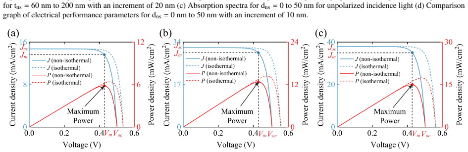
- If self-heating is included in a non-isothermal simulation, PCE drops by 13.77% to about 15.02%, so thermal management is part of realizing the headline number.
Reading between the lines
- The same Ag/AZO hybrid-nanostructure strategy could plausibly transfer to other thin absorbers such as perovskite or amorphous silicon, where parasitic absorption in metal nanoparticles is also a known loss; the paper does not test this.
- The 83.32% average absorption is an unweighted spectral average, so the more decision-relevant number is the AM1.5G-weighted $J_{sc}$; the paper's own parameter sweeps show that absorption and current do not always move together, since thicker Si absorbs more but yields less current.
- The comparative table mixes cells with different voltages and absorber thicknesses, so the efficiency lead is driven mainly by current density; a fairer comparison would hold recombination parameters and contact losses fixed.
- A fabricated device would likely show lower performance than the simulation because the model assumes idealized interfaces and treats ITO/AZO as metals in the charge-transport stage; the optical-to-electrical coupling is the part most sensitive to real-world material quality.
Signed reviews
Editorial analysis
A structured set of objections, weighed in public.
Referee Report
Summary. This manuscript presents a computational design for a thin-film c-Si/TiO2 heterojunction solar cell with a back reflector containing triangular Ag-AZO hybrid metal-dielectric nanostructures and front ITO/SiO2/TiO2 texturing. Optical performance is simulated with 3D FDTD, and electrical performance is simulated with Lumerical CHARGE. The authors report an average absorption of 83.32% over 300-1100 nm, Jsc = 37.96 mA/cm2, Voc = 0.56 V, FF = 0.82, and PCE = 17.42%, together with studies of polarization angle, incidence angle, structural parameter sweeps, self-heating effects, and a comparison among dielectric, metallic, and hybrid nanostructure pairs.
Significance. If the reported results are correct, the design is a useful light-trapping data point for thin c-Si heterojunction cells: the polarization tolerance (a maximum PCE variation of 0.34%) and the systematic parameter sweeps are valuable, and the use of standard FDTD/CHARGE workflows is appropriate. The strength of the paper lies in its breadth of parametric, angular, and thermal studies rather than in any new formalism. However, the central efficiency claims are currently not acceptable because of an ambiguity about which region is the photoactive layer and whether photons absorbed in TiO2 are counted as generating collected current.
major comments (4)
- [Section 3, Fig. 4] The statement that 'the photoactive layer for Structure III included both Si and TiO2 layers' directly contradicts Section 2, where the c-Si layer is described as the photoactive layer and the TiO2 inverted pyramid is described as the electron transport layer. The abstract compounds this by calling the 83.32% absorption that of a '1000 nm thick photoactive layer,' although the Structure III absorbing region includes the 80-nm TiO2 pyramid. This distinction is load-bearing: Eq. (3) defines absorptance for 'the photoactive layer,' and the generation rate passed to the CHARGE solver is obtained from the optical simulation (Section 2 and ESI Eq. (6)). If the optical generation rate includes photons absorbed in TiO2, then Jsc = 37.96 mA/cm2 and PCE = 17.42% are inflated, because the band diagram in Fig. 2 shows a large valence-band offset that blocks hole collection through TiO2; TiO2 cannot act as a photovoltaic absorber in this junction. Please report the Si-only absorptance spectrum and state explicitly whether the generation-rate profile is restricted to the Si volume; if it is not, the optical generation and all downstream electrical results must be recomputed.
- [Section 3.5] The comparison among np1 (AZO-AZO), np2 (Ag-Ag), and np3 (Ag-AZO) keeps 'all other structural parameters constant,' but the geometric parameters for the nanostructure pair (tns = 160 nm, bns = 50 nm, sns = 55 nm, dns = 10 nm) were optimized only for the hybrid pair, as described in Section 2 and ESI Figs. 13-14. The claimed 4.54% PCE improvement of np3 over np2 is therefore not a controlled comparison between optimally designed configurations; it may simply reflect that the geometry was tuned for the hybrid pair. Please re-optimize the metallic-only and dielectric-only pairs under the same protocol, or clearly state that the claimed enhancement is for a fixed geometry rather than for optimized structures.
- [Section 2 and Section 3.4] The CHARGE simulation configuration, including the recombination parameters (trap-assisted, radiative, Auger) and the modified drift-diffusion equations used for the non-isothermal self-heating study, is deferred to 'Section S3 of the ESI.' However, the version of the ESI under review contains only the structural-parameter optimization and optical-material-property sections; it does not include Section S3. Without those parameter values and equations, the reported Voc, FF, PCE, and the 13.77% non-isothermal degradation cannot be independently verified. Please include the full ESI Section S3 in the submission or move the essential material parameters and equations into the main text.
- [Eq. (4)] The 'average absorption' Aavg defined by Eq. (4) is a wavelength-unweighted mean over 300-1100 nm, but the text repeatedly labels it as 'average absorption for AM 1.5G.' Because the AM1.5G spectrum is strongly wavelength-dependent, the unweighted average is not a solar-weighted metric. Please either use a solar-weighted average or state explicitly that Aavg is unweighted, and adjust the abstract and the optical comparisons accordingly.
minor comments (5)
- [Section 3.1] The text reports that Aavg increases from 82.28% to 84.26% as the polarization angle rotates from 0° to 90°, while Jsc decreases from 38.02 to 37.88 mA/cm2; the qualitative explanation is plausible, but the apparent anti-correlation between the unweighted average absorption and the current should be quantified.
- [Table 2] Table 2 shows Jsc at θ = 60° (32.51 mA/cm2) is slightly larger than at θ = 50° (32.37 mA/cm2), despite the overall decreasing trend; please check this entry or comment on the non-monotonicity.
- [General] The manuscript contains numerous typographical artifacts, including 'e fficiency,' 'di fference,' 'incidence light,' and 'Fig. 4 (d) - (f) depict'; a thorough language and proofreading pass is needed.
- [Section 2] The phrase '12 perfectly matched steep-angle layers' is unclear; it presumably refers to steep-angle perfectly matched layer (PML) subregions, and the 'mesh accuracy of 3' setting should be defined.
- [ESI section numbering] The ESI section numbering is inconsistent: Section 2 refers to 'Section S3 of the ESI,' while Section 3.4 refers to 'Section 3 of ESI'; please standardize the references to the ESI.
Circularity Check
No significant circularity: the optical and electrical results are linked by a standard FDTD-to-CHARGE generation-transfer workflow, not by a fitted parameter or self-citation chain; the flagged photoactive-layer wording is a consistency concern, not a circular reduction.
full rationale
I walked the claimed derivation chain and found no step in which a headline result is defined in terms of another headline result, or in which a fitted parameter is renamed as a prediction. The optical absorptance Aavg is computed by FDTD via A(λ)=1−T(λ)−R(λ) (Section 2, Eqs. 1–3). The electrical Jsc and PCE are outputs of the CHARGE drift-diffusion solver, which receives the optical generation rate as a physical input ('After post-processing the generation rate data, we utilized this data as input for the Charge solver'). That is the normal, physically meaningful coupling between absorption and photocurrent, not a circular equivalence. The structural parameters were optimized using the optical Jsc formula in ESI Eq. (6), but reporting the performance of the optimized design is standard design optimization, not a hidden refit passed off as prediction. The 4.54% HMDN-vs-metallic enhancement is obtained while 'maintaining all other structural parameters constant' (Section 3.5), so it is a controlled counterfactual; it may not reflect a re-optimized metallic-only design, but that is a limitation of scope, not circularity. The main internal-consistency concern is that Section 3 defines the Structure III 'photoactive layer' as including both Si and TiO2, while Section 2 and the abstract describe a 1000 nm Si photoactive layer; this could affect whether TiO2 absorption is counted in the generation input and could inflate Jsc. That is a correctness/validity risk if the generation region includes TiO2, or a reporting inconsistency if it does not, but it is not a derivation that reduces by construction to its own inputs. There are no load-bearing self-citations, and Table 4 benchmarks against independent prior literature. Accordingly, the appropriate circularity finding is no significant circularity.
Assumptions & free parameters
free parameters (12)
- Unit cell period, P =
150 nm
- Si photoactive layer thickness, tSi =
1000 nm
- ITO planar layer thickness, tITO =
20 nm
- SiO2 layer thickness, tSiO2 =
140 nm
- TiO2 pyramid height, pTiO2 =
80 nm
- ITO pyramid height, pITO =
100 nm
- SiO2 pyramid height, pSiO2 =
100 nm
- Nanostructure base, bns =
50 nm
- Nanostructure side length, sns =
55 nm
- Nanostructure thickness, tns =
160 nm
- Distance between nanostructure pair, dns =
10 nm
- Doping concentration of p-Si and n-TiO2 =
1e13 cm-3
assumptions (7)
- standard math Maxwell's equations are solved by the FDTD method.
- standard math Drift-diffusion equations describe carrier transport.
- domain assumption AM1.5G spectrum is the illumination source.
- domain assumption Optical constants from Palik, DeVore, Konig, and Treharne are accurate.
- domain assumption ITO and AZO can be treated as metallic conductors in the charge solver.
- ad hoc to paper The photoactive layer for Structure III is defined to include the TiO2 layer.
- ad hoc to paper Sequential one-at-a-time parameter sweeps find a near-optimal design.
Cite this review
Pith. "Pith review of Efficiency Enhancement of c-Si/TiO$_2$ Heterojunction Thin Film Solar Cell Using Hybrid Metal-Dielectric Nanostructures." pith.science (2026). https://pith.science/paper/TEXAKUX7
@misc{pith2026241119925,
  author       = {Pith},
  title        = {Pith review of: Efficiency Enhancement of c-Si/TiO$_2$ Heterojunction Thin Film Solar Cell Using Hybrid Metal-Dielectric Nanostructures},
  year         = {2026},
  howpublished = {\url{https://pith.science/paper/TEXAKUX7}},
  note         = {Machine review of arXiv:2411.19925}
}
abstract
The hybrid metal-dielectric nanostructures (HMDN) are promising candidates to address the ohmic loss by conventional nanostructures in photovoltaic applications by strong confinement and high scattering directivity. In this study, we present a c-Si/TiO$_2$ heterojunction thin film solar cell (TFSC) where a pair of triangular HMDN comprised of Ag and AZO was utilized to enhance the longer wavelength light absorption. The presence of the TiO$_2$ inverted pyramid layer, in combination with the ITO and SiO$_2$-based pyramid layers at the front, enhanced the shorter wavelength light absorption by increasing the optical path and facilitating the coupling of incoming light in photonic mode. Consequently, the average absorption by 1000 nm thick photoactive layer reached 83.32 % for AM 1.5G within the wavelength range of 300 - 1100 nm which was investigated by employing the finite-difference time-domain (FDTD) method. The electric field profile and current density profile demonstrated the respective contributions of each layer in the absorption of light at shorter and longer wavelengths. The structure exhibited a short circuit current density ($J_{sc}$) of 37.96 mA/cm$^2$ and a power conversion efficiency ($PCE$) of 17.42 %. The efficiency of our proposed structure experienced a maximum relative change of 0.34 % when a polarized light was exposed with an angle of 0$^\circ$ to 90$^\circ$. The incorporation of self-heating in non-isothermal conditions reduced $PCE$ by $13.77 \%$. In addition, the comparative analysis to assess the impact of HMDN on our structure revealed a $4.54 \%$ increase in $PCE$ of the structure with metallic nanostructures, paving the way for the utilization of HMDN to enhance the performance of TFSC.
Figures


Figures from the paper (11 more)




Reference graph
Works this paper leans on
-
[1]
F. Qin, J. Chen, J. Liu, L. Liu, C. Tang, B. Tang, G. Li, L. Zeng, H. Li, Z. Yi, Design of high e fficiency perovskite solar cells based on inorganic and organic undoped double hole layer, Solar Energy 262 (2023) 111796
work page 2023
-
[2]
Y . He, Y . Tao, Z. Liu, Q. Huang, Design and optimization of nanostructure antireflection film for thin gaas solar cells based on the photoelectrical coupling model, Applied Energy 364 (2024) 123184. 15
work page 2024
-
[3]
A. K. Patel, R. Mishra, S. K. Soni, Electrical and optical pa- rameters optimization and interface engineering for e fficiency improvement of double cigs absorber based solar cell, Solar En- ergy 257 (2023) 125–136
work page 2023
-
[4]
J. Zheng, W. Duan, Y . Guo, Z. C. Zhao, H. Yi, F.-J. Ma, L. Granados Caro, C. Yi, J. Bing, S. Tang, J. Qu, K. C. Fong, X. Cui, Y . Zhu, L. Yang, A. Lambertz, M. Arafat Mahmud, H. Chen, C. Liao, G. Wang, M. Jankovec, C. Xu, A. Uddin, J. M. Cairney, S. Bremner, S. Huang, K. Ding, D. R. McKenzie, A. W. Y . Ho-Baillie, Efficient monolithic perovskite–si tande...
work page 2023
-
[5]
D. Pokhrel, X. Mathew, K. Khanal Subedi, A. Patel, A. B. Phillips, E. Bastola, A. Abudulimu, M. K. Jamarkattel, S. Ri- jal, A. Quader, J. Friedl, Z. Zawisza, Y . Yan, M. J. Heben, R. J. Ellingson, Bifacial cdte solar cells with copper chromium oxide back-buffer layer, Solar RRL 6 (11) (2022) 2200501
work page 2022
-
[6]
F. Zhao, Y . Yi, J. Lin, Z. Yi, F. Qin, Y . Zheng, L. Liu, F. Zheng, H. Li, P. Wu, The better photoelectric performance of thin-film tio2/c-si heterojunction solar cells based on surface plasmon res- onance, Results in Physics 28 (2021) 104628
work page 2021
-
[7]
Z. Sun, X. Chen, Y . He, J. Li, J. Wang, H. Yan, Y . Zhang, To- ward efficiency limits of crystalline silicon solar cells: Recent progress in high-e fficiency silicon heterojunction solar cells, Advanced Energy Materials 12 (23) (2022) 2200015
work page 2022
-
[8]
C. Ballif, F.-J. Haug, M. Boccard, P. J. Verlinden, G. Hahn, Status and perspectives of crystalline silicon photovoltaics in research and industry, Nature Reviews Materials 7 (8) (2022) 597–616
work page 2022
Show all 43 references
-
[9]
Moeini, G
S. Moeini, G. Abdi, H. Bahador, H. Heidarzadeh, High- performance a-si clustering nanohole arrays for solar photo- voltaics, Silicon 15 (8) (2023) 3497–3505
2023
-
[10]
El-Bashar, M
R. El-Bashar, M. Hussein, S. F. Hegazy, Y . Badr, B. M. A. Rah- man, K. T. V . Grattan, M. F. O. Hameed, S. S. A. Obayya, Elec- trical performance of efficient quad-crescent-shaped si nanowire solar cell, Scientific Reports 12 (1) (2022) 48
2022
-
[11]
Khaled, M
A. Khaled, M. F. O. Hameed, B. M. A. Rahman, K. T. V . Grat- tan, S. S. A. Obayya, M. Hussein, Characteristics of silicon nanowire solar cells with a crescent nanohole, Optics Express 28 (21) (2020) 31020–31033
2020
-
[12]
C. Wang, B. Ding, F. Bian, Y . Yang, S. M. Zaheer, T. Yu, Z. Li, H. Wang, Z. Xu, E ffects of frequency upconversion layer and two-dimensional arrays of inverted nanocone hole on the per- formance of ultrathin crystalline silicon solar cells, Optical Ma- terials 123 (2022) 111943
2022
-
[13]
D. V . Prashant, S. K. Agnihotri, D. P. Samajdar, Gaas nanocone array-based hybrid solar cells with excellent light-trapping capa- bilities and enhanced photogeneration rate, Semiconductor Sci- ence and Technology 37 (9) (2022) 095002
2022
-
[14]
F. Zhao, J. Lin, Z. Lei, Z. Yi, F. Qin, J. Zhang, L. Liu, X. Wu, W. Yang, P. Wu, Realization of 18.97% theoretical e fficiency of 0.9µm thick c-si/zno heterojunction ultrathin-film solar cells via surface plasmon resonance enhancement, Physical Chem- istry Chemical Physics 24 ...
2022
-
[15]
Oliveto, D.-A
V . Oliveto, D.-A. Borca-Tasciuc, Broadband asymmetric light transmission interfaces for luminescent solar concentrators, Nanoscale Advances 3 (12) (2021) 3627–3633
2021
-
[16]
Ibrahim, H
I. Ibrahim, H. N. Lim, N. W. K. Wan, N. M. Huang, S. P. Lim, W. Busayaporn, H. Nakajima, Plasmonic silver sandwich structured photoanode and reflective counter electrode enhanc- ing power conversion efficiency of dye-sensitized solar cell, So- lar Energy 215 (2021) 403–409
2021
-
[17]
Jamil, U
S. Jamil, U. Saha, M. K. Alam, Surface plasmon enhanced ultra- thin cu2znsns4/crystalline-si tandem solar cells, Nanoscale Ad- vances 5 (11) (2023) 2887–2896
2023
-
[18]
Rassekh, R
M. Rassekh, R. Shirmohammadi, R. Ghasempour, F. Razi As- taraei, S. Farjami Shayesteh, E ffect of plasmonic aluminum nanoparticles shapes on optical absorption enhancement in sili- con thin-film solar cells, Physics Letters A 408 (2021) 127509
2021
-
[19]
Lozac’h, S
M. Lozac’h, S. Nunomura, K. Matsubara, Double-sided topcon solar cells on textured wafer with ald siox layer, Solar Energy Materials and Solar Cells 207 (2020) 110357
2020
-
[20]
Meyer, A
F. Meyer, A. Savoy, J. J. Diaz Leon, M. Persoz, X. Niquille, C. Alleb ´e, S. Nicolay, F.-J. Haug, A. Ingenito, C. Ballif, Op- timization of front sinx /ito stacks for high-e fficiency two-side contacted c-si solar cells with co-annealed front and rear pas- sivating contacts, S...
2021
-
[21]
Y . A. Pritom, D. K. Sikder, S. Zaman, M. Hossain, Plasmon- enhanced parabolic nanostructures for broadband absorption in ultra-thin crystalline si solar cells, Nanoscale Advances 5 (18) (2023) 4986–4995
2023
-
[22]
X. Cui, Y . Chen, M. Zhang, Y . W. Harn, J. Qi, L. Gao, Z. L. Wang, J. Huang, Y . Yang, Z. Lin, Tailoring carrier dynamics in perovskite solar cells via precise dimension and architecture control and interfacial positioning of plasmonic nanoparticles, Energy & Environmental Sc...
2020
-
[23]
M. A. Alkhalayfeh, A. A. Aziz, M. Z. Pakhuruddin, An overview of enhanced polymer solar cells with embedded plas- monic nanoparticles, Renewable and Sustainable Energy Re- views 141 (2021) 110726
2021
-
[24]
Barreda, F
´A. Barreda, F. Vitale, A. E. Minovich, C. Ronning, I. Staude, Applications of hybrid metal-dielectric nanostructures: State of the art, Advanced Photonics Research 3 (4) (2022) 2100286
2022
-
[25]
R. Ren, Z. Zhong, Enhanced light absorption of silicon solar cells with dielectric nanostructured back reflector, Optics Com- munications 417 (2018) 110–114
2018
-
[26]
M. K. A. Mohammed, A. K. Al-Mousoi, S. Singh, U. Younis, A. Kumar, D. Dastan, G. Ravi, Ionic liquid passivator for meso- porous titanium dioxide electron transport layer to enhance the efficiency and stability of hole conductor-free perovskite solar cells, Energy & Fuels 36 (1...
2022
-
[27]
B. Wang, J. Yang, L. Lu, W. Xiao, H. Wu, S. Xiong, J. Tang, C. Duan, Q. Bao, Interface engineering of air-stable n-doping fullerene-modified tio2 electron transport layer for highly e ffi- cient and stable perovskite solar cells, Advanced Materials In- terfaces 7 (6) (2020) 1901964
2020
-
[28]
H. I. Elsaeedy, A. Qasem, H. A. Yakout, M. Mahmoud, The piv- otal role of tio2 layer thickness in optimizing the performance of tio2/p-si solar cell, Journal of Alloys and Compounds 867 (2021) 159150
2021
-
[29]
E. D. Palik, Handbook of optical constants of solids, V ol. 1 of Handbook of Optical Constants of Solids, 2012
2012
-
[30]
J. R. DeV ore, Refractive indices of rutile and sphalerite, Journal of the Optical Society of America 41 (6) (1951) 416–419
1951
-
[31]
T. A. F. K ¨onig, P. A. Ledin, J. Kerszulis, M. A. Mahmoud, M. A. El-Sayed, J. R. Reynolds, V . V . Tsukruk, Electrically tun- able plasmonic behavior of nanocube–polymer nanomaterials induced by a redox-active electrochromic polymer, ACS Nano 8 (6) (2014) 6182–6192
2014
-
[32]
R. E. Treharne, A. Seymour-Pierce, K. Durose, K. Hutchings, S. Roncallo, D. Lane, Optical design and fabrication of fully sputtered cdte/cds solar cells, Journal of Physics: Conference Series 286 (1) (2011) 012038
2011
-
[33]
P. P. Nakti, D. Sarker, M. I. Tahmid, A. Zubair, Ultra-broadband near-perfect metamaterial absorber for photovoltaic applica- tions, Nanoscale Advances 5 (24) (2023) 6858–6869
2023
-
[34]
Nelson, The Physics of Solar Cells, PUBLISHED BY IMPE- RIAL COLLEGE PRESS AND DISTRIBUTED BY WORLD SCIENTIFIC PUBLISHING CO., 2003
J. Nelson, The Physics of Solar Cells, PUBLISHED BY IMPE- RIAL COLLEGE PRESS AND DISTRIBUTED BY WORLD SCIENTIFIC PUBLISHING CO., 2003. 16
2003
-
[35]
A. A. Tabrizi, A. Pahlavan, Efficiency improvement of a silicon- based thin-film solar cell using plasmonic silver nanoparticles and an antireflective layer, Optics Communications 454 (2020) 124437
2020
-
[36]
A. S. Mohsin, S. Mondal, M. Mobashera, A. Malik, M. Islam, M. Rubaiat, E fficiency improvement of thin film solar cell us- ing silver pyramids array and antireflective layer, Heliyon 9 (6) (2023) e16749
2023
-
[37]
Shahabi, H
T. Shahabi, H. Heidarzadeh, H. Bahador, Dual metallic-based plasmonic back reflector to broaden the absorption spectra of a thin film amorphous silicon solar cell, Optics Communications 544 (2023) 129623
2023
-
[38]
Saravanan, R
S. Saravanan, R. S. Dubey, Y . Venkatesh, The role of photonic and plasmonic modes in ultrathin amorphous silicon solar cells using finite di fference time domain method, Materials Today: Proceedings 64 (2022) 1666–1670
2022
-
[39]
G. Abdi, H. Bahador, Full wavelengths absorption enhancement of an ultra-thin film si /a-si solar cell using upright stuck spher- ical plasmonic nanoparticles, Plasmonics 17 (4) (2022) 1775– 1782
2022
-
[40]
F. E. Subhan, A. D. Khan, F. E. Hilal, A. D. Khan, S. D. Khan, R. Ullah, M. Imran, M. Noman, E fficient broadband light ab- sorption in thin-film a-si solar cell based on double sided hybrid bi-metallic nanogratings, RSC Advances 10 (20) (2020) 11836– 11842
2020
-
[41]
Heidarzadeh, A
H. Heidarzadeh, A. Jangjoy, H. Bahador, Use of coupled al-ag bimetallic cylindrical nanoparticles to improve the photocurrent of a thin-film silicon solar cell, Plasmonics 17 (3) (2022) 1323– 1329. 17 Electronic Supplementary Information (ESI)
2022
-
[42]
We have conducted these operations several times to get an op- timized performance
Structural Parameters Optimization The structural parameters were optimized by utilizing the short circuit current density, Jsc obtained from the optical simulation, using the following equation, Jsc = e Z λ hc QE(λ)IAM1.5(λ)dλ (6) We optimized the thicknesses of the front lay...
-
[43]
The speed of the light is controlled by the value of n, while κ determines how much the light will be scattered and absorbed
Material properties Figure 15 illustrates both the adopted and FDTD fit- ted optical properties of Ag, AZO, ITO, Si, SiO 2, and TiO2 which include both the refractive index (n), and the extinction coefficient (κ). The speed of the light is controlled by the value of n, while κ...
Reviewed August 12, 2026 · model on record in the stance chip above.
Discussion (0). Continue with ORCID to comment.