REVIEW 3 major objections 5 minor 79 references
Enabling and Exploiting Partition-Level Parallelism (PALP) in Phase Change Memories
T0 review · 3 major / 5 minor · reviewed 2026-08-14 · deepseek-v4-flash
Pith's one-line read A phase-change memory bank can serve two conflicting reads or a read and a write at once by activating two partitions, and a new scheduler exploits this to cut average access latency by 23%.
desk verdict Genuinely new mechanism for read-read parallelism in PCM banks, but the headline gains hinge on an unvalidated circuit assumption that the write driver's verify logic can serve as a second sense amplifier. read the letter →
The pith
A machine-rendered reading of the paper's core claim, the machinery that carries it, and where it could break.
The reading
What carries the argument
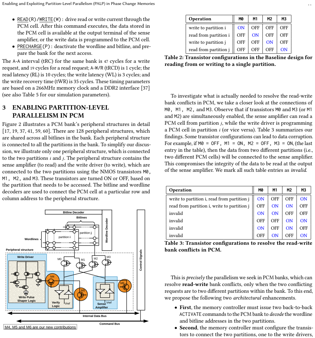
The load-bearing mechanism is the pairing of two partitions through the bank's 128 shared peripheral structures. Each peripheral structure holds a sense amplifier and a write driver whose verify logic can be electrically decoupled (transistor M4) to act as a second sense amplifier; two extra transistors (M5, M6) arbitrate the internal data bus so both read results can be transferred serially in 8+1+8 cycles. Two new commands encode the pairing: READ-WITH-WRITE (RWW) connects one partition to the sense amplifiers and another to the write drivers, and READ-WITH-READ (RWR), preceded by DECOUPLE, connects two partitions to the two sensing circuits. On top of this, a memory-controller scheduler selects, from a FIFO read-write queue, the oldest request that can pair with the request being served, estimates the power of the concurrent schedule against the RAPL limit, and falls back to serving one request alone if power would be exceeded or reordering would cause starvation. This machinery converts bank conflicts, which average 43% of PCM requests in the evaluated workloads and are mostly read-read, from serialized delays into overlapped operations.
What would settle it
Measure, in a 20nm PCM test chip or transistor-level simulation, the sensing margin and delay of the verify logic configured as a sense amplifier while the real sense amplifier reads from another partition on the same bank. If the verify logic cannot reliably resolve a SET versus RESET cell within 10 cycles, or if the concurrent read introduces bit errors, the RWR command and the reported 28% improvement fail.
Extended reading notes
Core claim
The core discovery is that a PCM bank's partitions can operate concurrently when the bank's shared peripheral structures are split between them, and the limits of that concurrency are set by the number of peripheral structures (here, two partitions at once). For a read-write conflict, the sense amplifier can read from one partition while the write driver programs another, using the new RWW command; the write recovery time of the write overlaps with the read latency, cutting service time from 66 to 48 cycles. For a read-read conflict, the write driver's verify logic, which already contains cross-coupled inverters, is decoupled by a transistor (M4) and used as a second sense amplifier, so two reads proceed in parallel under the new RWR command, cutting service time from 38 to 30 cycles. The paper further claims that a scheduler which prioritizes requests that can pair up, while enforcing a starvation threshold and a running-average-power limit, is needed to convert these circuit-level savings into system-level gains. On their evaluated 8-core DRAM-PCM workloads, the combination yields 23% lower average access latency and 28% better performance than the MultiPartition baseline, which resolves only read-write conflicts.
Load-bearing premise
The read-read mechanism assumes that the write driver's verify logic, once decoupled by transistor M4, can serve as a sense amplifier that is fast enough (10-cycle read latency), sensitive enough to resolve the PCM cell's resistance, and isolated enough not to disturb or be disturbed by the data being read by the real sense amplifier.
Editorial extensions
If this is right
- Read-read bank conflicts, which make up 34% of all PCM requests (79% of all conflicts), become resolvable, so the most common serialization in these workloads is removed.
- Because the scheduler pairs requests deliberately, simply adding RWW/RWR commands to a first-come-first-served controller yields little benefit; the scheduling policy is what turns the hardware capability into the reported 28% gain.
- PALP stays within the PCM's RAPL limit by estimating the added power of concurrent partitions and serializing when needed, so the parallelism does not come at the cost of violating the power budget.
- The mechanism transfers across DDR2 and DDR4 interfaces and across PCM capacities and eDRAM write-cache sizes, and it can be composed with write-reduction and endurance techniques.
- The 1.15% area overhead per peripheral structure and the critical-path delay of 1453ps (below the 3.9ns clock period) indicate the extra logic does not limit the rated memory clock.
Reading between the lines
- If the verify-logic-as-sense-amplifier trick is sound, the same decoupling idea could apply to other program-and-verify resistive memories (for example, RRAM or MRAM arrays) that share peripheral structures among sub-arrays, giving a general template for turning verify circuits into parallel read paths.
- The scheduler's power-estimation equation suggests a testable extension: the RAPL limit can be treated as a tunable knob that trades a few percent of performance for a measurable power reduction, which the paper's sweep already hints at for limits below 0.4 pJ/access.
- Because the two active partitions share bitline and wordline decoders only through the peripheral structures, PALP's benefit should scale with the number of partitions per bank; a bank with more partitions could in principle support more than two concurrent accesses if peripheral structures were added, which the paper does not explore.
- The data-transfer arbitration (8+1+8 cycles) is a serialization point; overlapping the two data transfers or widening the internal bus could further cut RWR latency, a direction the paper leaves implicit.
Signed reviews
Editorial analysis
A structured set of objections, weighed in public.
Referee Report
Summary. The paper proposes PALP, a mechanism that enables and exploits partition-level parallelism inside a PCM bank. It introduces a READ-WITH-WRITE (RWW) command to overlap a read and a write to different partitions, and a READ-WITH-READ (RWR) command, together with a decoupling transistor M4 and data-bus switches M5/M6, that lets the write driver's verify logic operate as a second sense amplifier to overlap two reads. A new memory-controller scheduling policy prioritizes requests that can exploit this parallelism, while enforcing a starvation threshold and a running-average-power-limit (RAPL). The evaluation uses a gem5+Ramulator-based full-system simulator with IBM 20nm PCM timing parameters and MiBench/SPEC CPU2017/mixed workloads, reporting 23% average PCM access-latency reduction and 28% average execution-time improvement over MultiPartition, plus sensitivity studies across eDRAM size, PCM capacity, DDR2/DDR4 interfaces, RAPL limit, and backlogging threshold.
Significance. The paper addresses a real and measurable bottleneck: read-read conflicts dominate PCM bank conflicts (34% of all PCM requests, 79% of all bank conflicts), and Figure 16 shows that resolving read-read conflicts is what turns a 7% improvement over Baseline into 32.2%. If the RWR circuit mechanism works, PALP is a genuinely novel architectural contribution: it is the first, to my knowledge, to resolve read-read bank conflicts in PCM with a reported area overhead of 1.15% per peripheral structure, and the proposed scheduling policy with explicit starvation and RAPL checks is a useful step beyond FCFS. The work is also reproducible: the simulator is open-sourced, and the sensitivity analysis (eDRAM size, PCM capacity, DDR2/DDR4, RAPL and threshold sweeps, SPICE overheads) is unusually thorough for an architecture paper. The central results are, however, conditional on two load-bearing assumptions: the verify logic can function as a sense amplifier, and the new command timings (48 and 30 cycles) are realizable. These assumptions are not validated at the circuit or command-timing level, so the headline 28% number is conditional on them.
major comments (3)
- [Section 3.2 and Section 6.5] The RWR mechanism is not validated at the circuit level. The paper asserts that the write driver's verify logic 'essentially consists of two cross-coupled inverters, which can be configured as a sense amplifier' and that adding transistor M4 is sufficient, but a working PCM sense amplifier requires a reference, offset compensation, adequate sensing margin, and isolation from the concurrently sensed partition. The SPICE study in Section 6.5 measures only critical-path delay, power, and area of one peripheral structure; it does not demonstrate that the verify logic can resolve a PCM cell's state within the assumed 10-cycle read latency, nor that it does not disturb the sense amplifier's concurrent read. Because Figure 16 attributes the jump from 7% to 32.2% improvement over Baseline to read-read resolution, the headline performance claim is conditional on this unvalidated circuit assumption. Please add functional mixed-signal validation of the decoupled verify-logic read path, including two-partition simultaneous reads and process variation, or explicitly re-frame the RWR results as conditional on this assumption.
- [Section 3.1, Section 3.2, and Table 5] The new command service times A-RWW-P=48 and A-RWR-P=30 cycles are assumed rather than derived from validated timing analysis. In Figure 3, the RWW timing assumes a 10-cycle read can overlap with a 35-cycle write, with only a 1-cycle setup for the second ACTIVATE and no additional delay for shared-peripheral contention; in Figure 4, the RWR timing assumes two reads can be resolved in 10 cycles plus a 17-cycle serialized data transfer. These are plausible constructions from the baseline PCM timings, but the simulator embeds them as fixed parameters, so the 23%/28% results are conditional on them. The paper should provide a command-level timing analysis against a validated PCM timing model or a sensitivity analysis over these two parameters.
- [Section 6.4 and Section 6.9.1] The RAPL configuration is internally inconsistent: Section 6.4 and Figure 10 state the RAPL limit is 0.4 pJ/access, while Section 6.9.1 and Figure 14 describe the default RAPL limit as 0.3 pJ/access and later refer to the 'rated value of 0.4 pJ/access.' Since the claim that PALP stays within the RAPL limit and the conclusions of the RAPL sweep depend on the actual limit used, this inconsistency must be resolved in the revised manuscript.
minor comments (5)
- [Abstract and Section 3.1] The abstract says the first contribution requires 'minimal changes' to PCM logic and interface, while Section 3.1 claims 'no changes needed to PCM logic or its interface,' and Section 3.2 introduces M4/M5/M6. Please harmonize these statements.
- [Section 4.3] The sentence 'This reduces the total PCM service latency to 126 cycles, a further savings of 12.5% compared to ❸' should compare schedule ❸ to schedule ❷ (144 cycles), not to itself.
- [Section 6.9.1] The sentence 'We observe that for bwaves, setting the RAPL limit to 0.2 pJ/access results in a performance improvement of only 11% over the Baseline, compared to the 33% when RAPL limit is set to 0.4pJ/access' is confusing because the figure's default is 0.3 pJ/access; please clarify which RAPL value is the default and which is the rated value.
- [Equation 1 and Table 5] Equation 1 uses PSA and PWD, but the paper does not report their values or clarify whether they represent total bank power or per-peripheral-structure power; please provide these values and definitions.
- [Section 4.3] The text says 'Overall, PALP improves performance by 25.8% over the baseline ❷ in this example,' but the baseline is schedule ❶, not ❷; please correct the cross-reference.
Circularity Check
No circular derivation: PALP's speedups are computed by a simulator from stated PCM timings and workload traces, not recovered from fitted parameters or self-citations.
full rationale
The paper's central claim—that resolving read-read and read-write bank conflicts at partition granularity improves performance—is derived by simulation from IBM PCM timing parameters (Table 5), external benchmark traces (MiBench and SPEC CPU2017), and the authors' new command timings (A-RWW-P=48 cycles, A-RWR-P=30 cycles). These timings are constructed from baseline read/write latencies (Figures 3 and 4 show the cycle arithmetic), and the scheduler is then evaluated on external workloads; no parameter is fitted to the headline 23% and 28% numbers. The RWW/RWR circuit proposal is an engineering assumption—specifically, that the verify logic's cross-coupled inverters can serve as a sense amplifier—but this is a correctness and validity risk, not a circular reduction: the paper does not define RWR success in terms of the performance result. The SPICE study covers only critical-path delay, power, and area of one peripheral structure, so the functional readout assumption remains unvalidated, but that missing support is not circularity. Self-references are limited to the open-source simulator repository [57] and to prior work [28] as inspiration, and neither is load-bearing for the quantitative claim. The comparison against MultiPartition [71] implements that prior technique with DDR4 timing, which is a fair re-implementation rather than a self-citation. Therefore no step in the derivation chain is equivalent to its input by construction.
Assumptions & free parameters
free parameters (5)
- Backlogging threshold (th_b) =
8 accesses (swept 2 to 16)
- RWW service time (A-RWW-P) =
48 cycles
- RWR service time (A-RWR-P) =
30 cycles
- RAPL limit =
0.4 pJ/access (Section 6.4) vs 0.3 pJ/access (Section 6.9.1)
- PSA and PWD (power of sense amplifiers and write drivers)
assumptions (4)
- domain assumption A PCM bank is organized into partitions that share a small number of peripheral structures (sense amplifiers and write drivers).
- ad hoc to paper The write driver's verify logic can be decoupled and operated as a sense amplifier for reads.
- domain assumption Two simultaneously active partitions do not cause electrical disturb, data corruption, or timing violations.
- domain assumption The modeled DDR4/DDR2 interface and timings from IBM's 20nm PCM prototype are representative of a modern PCM device.
Cite this review
Pith. "Pith review of Enabling and Exploiting Partition-Level Parallelism (PALP) in Phase Change Memories." pith.science (2026). https://pith.science/paper/X4UM5LBC
@misc{pith2026190807966,
  author       = {Pith},
  title        = {Pith review of: Enabling and Exploiting Partition-Level Parallelism (PALP) in Phase Change Memories},
  year         = {2026},
  howpublished = {\url{https://pith.science/paper/X4UM5LBC}},
  note         = {Machine review of arXiv:1908.07966}
}
read the original abstract
Phase-change memory (PCM) devices have multiple banks to serve memory requests in parallel. Unfortunately, if two requests go to the same bank, they have to be served one after another, leading to lower system performance. We observe that a modern PCM bank is implemented as a collection of partitions that operate mostly independently while sharing a few global peripheral structures, which include the sense amplifiers (to read) and the write drivers (to write). Based on this observation, we propose PALP, a new mechanism that enables partition-level parallelism within each PCM bank, and exploits such parallelism by using the memory controller's access scheduling decisions. PALP consists of three new contributions. First, we introduce new PCM commands to enable parallelism in a bank's partitions in order to resolve the read-write bank conflicts, with minimal changes needed to PCM logic and its interface. Second, we propose simple circuit modifications that introduce a new operating mode for the write drivers, in addition to their default mode of serving write requests. When configured in this new mode, the write drivers can resolve the read-read bank conflicts, working jointly with the sense amplifiers. Finally, we propose a new access scheduling mechanism in PCM that improves performance by prioritizing those requests that exploit partition-level parallelism over other requests, including the long outstanding ones. While doing so, the memory controller also guarantees starvation-freedom and the PCM's running-average-power-limit (RAPL). We evaluate PALP with workloads from the MiBench and SPEC CPU2017 Benchmark suites. Our results show that PALP reduces average PCM access latency by 23%, and improves average system performance by 28% compared to the state-of-the-art approaches.
Figures


Figures from the paper (12 more)


Reference graph
Works this paper leans on
-
[1]
Shoaib Akram, Jennifer B Sartor, Kathryn S McKinley, and Lieven Eeckhout
-
[2]
Kandemir, Anand Sivasubramaniam, and Chita R
Mohammad Arjomand, Mahmut T. Kandemir, Anand Sivasubramaniam, and Chita R. Das. 2016. Boosting Access Parallelism to PCM-based Main Memory. In International Symposium on Computer Architecture (ISCA)
work page 2016
-
[3]
Alasdair Armstrong, Thomas Bauereiss, Brian Campbell, Alastair Reid, Kathryn E. Gray, Robert M. Norton, Prashanth Mundkur, Mark Wassell, Jon French, Christo- pher Pulte, Shaked Flur, Ian Stark, Neel Krishnaswami, and Peter Sewell. 2019. ISA Semantics for ARMv8-a, RISC-v, and CHERI-MIPS. Proceedings of the ACM on Programming Languages (POPL) 3, Article 71 (2019)
work page 2019
-
[4]
JEDEC Solid State Technology Association et al. 2012. JEDEC Standard: DDR4 SDRAM. JESD79-4, Sep (2012)
work page 2012
-
[5]
Gerald John Barkley, Daniele Vimercati, and Pierguido Garofalo. 2017. Apparatus and methods to perform read-while write (RWW) operations. US Patent App. 15/688,667
work page 2017
-
[6]
Nathan Binkert, Bradford Beckmann, Gabriel Black, Steven K Reinhardt, Ali Saidi, Arkaprava Basu, Joel Hestness, Derek R Hower, Tushar Krishna, Somayeh Sardashti, et al. 2011. The gem5 simulator. ACM SIGARCH Computer Architecture News 39, 2 (2011)
work page 2011
-
[7]
Santiago Bock, Bruce R Childers, Rami Melhem, and Daniel Mossé. 2016. Con- current migration of multiple optoptpages in software-managed hybrid main memory. In International Conference on Computer Design (ICCD)
work page 2016
-
[8]
James Bucek, Klaus-Dieter Lange, et al. 2018. SPEC CPU2017: Next-Generation Compute Benchmark. In International Conference on Performance Engineering (ICPE)
work page 2018
Show all 79 references
-
[9]
Castellani, G
N. Castellani, G. Navarro, V. Sousa, P. Zuliani, R. Annunziata, M. Borghi, L. Perniola, and G. Reimbold. 2016. Comparative Analysis of Program/Read Disturb Robustness for GeSbTe-Based Phase-Change Memory Devices. In International Memory Workshop (IMW)
2016
-
[10]
Karthik Chandrasekar, Christian Weis, Yonghui Li, Benny Akesson, Norbert Wehn, and Kees Goossens. 2012. DRAMPower: Open-source DRAM power & energy estimation tool. URL: http://www. drampower. info (2012)
2012
-
[11]
Baek-Hyung Cho, Woo-Yeong Cho, Hyung-Rok Oh, and Byung-Gil Choi. 2005. Programming method of controlling the amount of write current applied to phase change memory device and write driver circuit therefor. US Patent 6,885,602
2005
-
[12]
Sangyeun Cho and Hyunjin Lee. 2009. Flip-N-Write: a simple deterministic tech- nique to improve PRAM write performance, energy and endurance. InSymposium on Microarchitecture (MICRO)
2009
-
[13]
Howard David, Eugene Gorbatov, Ulf R Hanebutte, Rahul Khanna, and Chris- tian Le. 2010. RAPL: memory power estimation and capping. In International Symposium on Low Power Electronics and Design (ISLPED)
2010
-
[14]
Gaurav Dhiman, Raid Ayoub, and Tajana Rosing. 2009. PDRAM: A hybrid PRAM and DRAM main memory system. In Design Automation Conference (DAC)
2009
-
[15]
Cyrille Dray and Liqiong Wei. 2018. High voltage tolerant word-line driver. US Patent 9,875,783
2018
-
[16]
Khaled El Emam, Walcelio Melo, and Jean-Normand Drouin. 1997. SPICE: The theory and practice of software process improvement and capability determination
1997
-
[17]
Jean-Jacques Fagot, Philippe Boivin, Vincenzo Della-Marca, Jeremie Postel- Pellerin, Damien Deleruyelle, Olivier Weber, Emmanuel Richard, and Franck Arnaud. 2018. Low Cost Diode as Selector Device for Embedded Phase Change Memory in Advanced FD-SOI Technology. In International...
2018
-
[18]
Saugata Ghose, Tianshi Li, Nastaran Hajinazar, Damla Senol Cali, and Onur Mutlu
-
[19]
Akira Goda, Tommaso Vali, Carmine Miccoli, and Pranav Kalavade. 2018. Pro- gramming memory devices. US Patent App. 15/477,048
2018
-
[20]
Matthew R Guthaus, Jeffrey S Ringenberg, Dan Ernst, Todd M Austin, Trevor Mudge, and Richard B Brown. 2001. MiBench: A free, commercially representative embedded benchmark suite. In Workshop on workload characterization (WWC)
2001
-
[21]
Tae Jun Ham, Bharath K Chelepalli, Neng Xue, and Benjamin C Lee. 2013. Dis- integrated control for energy-efficient and heterogeneous memory systems. In High Performance Computer Architecture (HPCA)
2013
-
[22]
Hasan Hassan, Minesh Patel, Jeremie S Kim, A Giray Yaglikci, Nandita Vijayku- mar, Nika Mansouri Ghiasi, Saugata Ghose, and Onur Mutlu. 2019. CROW: A Low-Cost Substrate for Improving DRAM Performance, Energy Efficiency, and Reliability. In International Symposium on Computer A...
2019
-
[23]
Hasan Hassan, Gennady Pekhimenko, Nandita Vijaykumar, Vivek Seshadri, Donghyuk Lee, Oguz Ergin, and Onur Mutlu. 2016. ChargeCache: Reducing DRAM latency by exploiting row access locality. In High Performance Computer Architecture (HPCA)
2016
-
[24]
Jingtong Hu, Chun Jason Xue, Qingfeng Zhuge, Wei-Che Tseng, and Edwin H-M Sha. 2013. Write activity reduction on non-volatile main memories for embedded chip multiprocessors. ACM Transactions on Embedded Computing 12, 3 (2013)
2013
-
[25]
Yazhi Huang, Tiantian Liu, and Chun Jason Xue. 2011. Register aloptlocation for write activity minimization on non-volatile main memory. In Asia South Pacific Design Automation Conference (ASP-DAC)
2011
-
[26]
Lei Jiang, Youtao Zhang, Bruce R Childers, and Jun Yang. 2012. FPB: Fine-grained power budgeting to improve write throughput of multi-level cell phase change memory. In Symposium on Microarchitecture (MICRO)
2012
-
[27]
Yoongu Kim, Dongsu Han, Onur Mutlu, and Mor Harchol-Balter. 2010. ATLAS: A scalable and high-performance scheduling algorithm for multiple memory controllers. In High Performance Computer Architecture (HPCA)
2010
-
[28]
Yoongu Kim, Vivek Seshadri, Donghyuk Lee, Jamie Liu, and Onur Mutlu. 2012. A Case for Exploiting Subarray-level Parallelism (SALP) in DRAM. In International Symposium on Computer Architecture (ISCA)
2012
-
[29]
Yoongu Kim, Weikun Yang, and Onur Mutlu. 2016. Ramulator: A Fast and Extensible DRAM Simulator. Computer Architecture Letters 15, 1 (2016)
2016
-
[30]
Lee, Engin Ipek, Onur Mutlu, and Doug Burger
Benjamin C. Lee, Engin Ipek, Onur Mutlu, and Doug Burger. 2009. Architect- ing Phase Change Memory As a Scalable Dram Alternative. In International Symposium on Computer Architecture (ISCA)
2009
-
[31]
Benjamin C Lee, Engin Ipek, Onur Mutlu, and Doug Burger. 2010. Phase change memory architecture and the quest for scalability. Commun. ACM 53, 7 (2010)
2010
-
[32]
B. C. Lee, P. Zhou, J. Yang, Y. Zhang, B. Zhao, E. Ipek, O. Mutlu, and D. Burger
-
[33]
Chang Joo Lee, Veynu Narasiman, Eiman Ebrahimi, Onur Mutlu, and Yale N Patt. 2010. DRAM-aware last-level cache writeback: Reducing write-caused interference in memory systems. (2010)
2010
-
[34]
Yang Li, Saugata Ghose, Jongmoo Choi, Jin Sun, Hui Wang, and Onur Mutlu. 2017. Utility-based hybrid memory management. In Conference on Cluster Computing (CLUSTER)
2017
-
[35]
Ye-Jyun Lin, Chia-Lin Yang, Hsiang-Pang Li, and Cheng-Yuan Michael Wang
-
[36]
Sihang Liu, Aasheesh Kolli, Jinglei Ren, and Samira Khan. 2018. Crash Consistency in Encrypted Non-volatile Main Memory Systems. InHigh Performance Computer Architecture (HPCA)
2018
-
[37]
Hsiang-Lan Lung, Christopher P Miller, Chia-Jung Chen, Scott C Lewis, Jack Morrish, Tony Perri, Richard C Jordan, Hsin-Yi Ho, Tu-Shun Chen, Wei-Chih Chien, et al. 2016. A double-data-rate 2 (DDR2) interface phase-change memory with 533MB/s read-write data rate and 37.5 ns acce...
2016
-
[38]
Justin Meza, Jichuan Chang, HanBin Yoon, Onur Mutlu, and Parthasarathy Ran- ganathan. 2012. Enabling efficient and scalable hybrid memories using fine- granularity DRAM cache management. Computer Architecture Letters 11, 2 (2012)
2012
-
[39]
Justin Meza, Yixin Luo, Samira Khan, Jishen Zhao, Yuan Xie, and Onur Mutlu
-
[40]
DDR Micron. 2014. SDRAM, 4Gb: x4, x8, x16 DDR4 SDRAM Features, white paper. Micron Technology, Inc (2014)
2014
-
[41]
Gabriele Navarro, Guillaume Bourgeois, Julia Kluge, Anna Lisa Serra, Anthonin Verdy, Julien Garrione, Marie-Claire Cyrille, Nicolas Bernier, Audrey Jannaud, Chiara Sabbione, et al. 2018. Phase-Change Memory: Performance, Roles and Challenges. In International Memory Workshop (IMW)
2018
-
[42]
T Nirschl, JB Philipp, TD Happ, Geoffrey W Burr, B Rajendran, M-H Lee, A Schrott, M Yang, M Breitwisch, C-F Chen, et al. 2007. Write strategies for 2 and 4-bit multi-level phase-change memory. In International Electron Devices Meeting (IEDM)
2007
-
[43]
Ovshinsky
S. Ovshinsky. 1968. Reversible electrical switching phenomena in disordered structures. Physical Review Letters (1968)
1968
-
[44]
Reena Panda, Shuang Song, Joseph Dean, and Lizy K John. 2018. Wait of a decade: Did SPEC CPU 2017 broaden the performance horizon?. In High Performance Computer Architecture (HPCA)
2018
-
[45]
Bahareh Pourshirazi, Majed Valad Beigi, Zhichun Zhu, and Gokhan Memik
-
[46]
Bahareh Pourshirazi, Majed Valad Beigi, Zhichun Zhu, and Gokhan Memik. 2019. Writeback-Aware LLC Management for PCM-Based Main Memory Systems.ACM Transactions on Design Automation of Electronic Systems 24, 2 (2019)
2019
-
[47]
Qureshi, Michele M
Moinuddin K. Qureshi, Michele M. Franceschini, Ashish Jagmohan, and Luis A. Lastras. 2012. PreSET: Improving Performance of Phase Change Memories by Exploiting Asymmetry in Write Times. In International Symposium on Computer Architecture (ISCA)
2012
-
[48]
Qureshi, Michele M
Moinuddin K. Qureshi, Michele M. Franceschini, Luis A. Lastras-Montaño, and John P. Karidis. 2010. Morphable Memory System: A Robust Architecture for Exploiting Multi-level Phase Change Memories. In International Symposium on Computer Architecture (ISCA)
2010
-
[49]
Moinuddin K Qureshi, Michele M Franceschini, and Luis A Lastras-Montano. 2010. Improving read performance of phase change memories via write cancellation and write pausing. In High Performance Computer Architecture (HPCA)
2010
-
[50]
Qureshi, Vijayalakshmi Srinivasan, and Jude A
Moinuddin K. Qureshi, Vijayalakshmi Srinivasan, and Jude A. Rivers. 2009. Scal- able High Performance Main Memory System Using Phase-change Memory Technology. In International Symposium on Computer Architecture (ISCA)
2009
-
[51]
In Design, Automation & Test in Europe Conference & Exhibition (DATE)
WALL: A writeback-aware LLC management for PCM-based main memory systems. In Design, Automation & Test in Europe Conference & Exhibition (DATE)
-
[52]
Bal S Sandhu, Cezary Pietrzyk, and George McNeil Lattimore. 2018. Memory write driver, method and system. US Patent App. 15/904,848
2018
-
[53]
P Schuddinck, M Badaroglu, M Stucchi, S Demuynck, A Hikavyy, M Garcia- Bardon, A Mercha, A Mallik, T Chiarella, S Kubicek, et al. 2012. Standard cell level parasitics assessment in 20nm BPL and 14nm BFF. In International Electron Devices Meeting (IEDM)
2012
-
[54]
Nak Hee Seong, Dong Hyuk Woo, and Hsien-Hsin S. Lee. 2010. Security Refresh: Prevent Malicious Wear-out and Increase Durability for Phase-change Memory with Dynamically Randomized optaddress Mapping. In International Symposium on Computer Architecture (ISCA)
2010
-
[55]
Gibbons, Michael A
Vivek Seshadri, Abhishek Bhowmick, Onur Mutlu, Phillip B. Gibbons, Michael A. Kozuch, and Todd C. Mowry. 2014. The Dirty-block Index. In International Symposium on Computer Architecture (ISCA)
2014
-
[56]
Saurabh Sinha, Greg Yeric, Vikas Chandra, Brian Cline, and Yu Cao. 2012. Ex- ploring sub-20nm FinFET design with predictive technology models. In Design Automation Conference (DAC)
2012
-
[57]
Dally, Ujval J
Scott Rixner, William J. Dally, Ujval J. Kapasi, Peter Mattson, and John D. Owens
-
[58]
Hunter, and Lizy K
Jeffrey Stuecheli, Dimitris Kaseridis, David Daly, Hillery C. Hunter, and Lizy K. John. 2010. The Virtual Write Queue: Coordinating DRAM and Last-level Cache Policies. In International Symposium on Computer Architecture (ISCA)
2010
-
[59]
C. Villa. 2018. PCM Array Architecture and Management. In Phase Change Memory
2018
-
[60]
Corrado Villa, Duane Mills, Gerald Barkley, Hari Giduturi, Stefan Schippers, and Daniele Vimercati. 2010. A 45nm 1Gb 1.8 V phase-change memory. In International Solid-State Circuits Conference Digest of Technical Papers (ISSCC)
2010
-
[61]
Zhe Wang, Shuchang Shan, Ting Cao, Junli Gu, Yi Xu, Shuai Mu, Yuan Xie, and Daniel A Jiménez. 2013. WADE: Writeback-aware dynamic cache management for NVM-based main memory system. ACM Transactions on Architecture and Code Optimization (TACO) 10, 4 (2013)
2013
-
[62]
Fei Xia, Dejun Jiang, Jin Xiong, Mingyu Chen, Lixin Zhang, and Ninghui Sun
-
[63]
Shiying Xiong and Jeffrey Bokor. 2003. Sensitivity of double-gate and FinFETDe- vices to process variations. IEEE Transactions on Electron Devices 50, 11 (2003)
2003
-
[64]
Shihao Song, Anup Das, Onur Mutlu, and Nagrajan Kandasamy. 2019. Enabling and Exploiting Partition-Level Parallelism (PALP) in Phase Change Memories. https: //github.com/drexel-DISCO/PALP
2019
-
[65]
Hanbin Yoon, Justin Meza, Naveen Muralimanohar, Norman P Jouppi, and Onur Mutlu. 2015. Efficient data mapping and buffering techniques for multilevel cell phase-change memories. ACM Transactions on Architecture and Code Optimization (TACO) 11, 4 (2015)
2015
-
[66]
Xiangyao Yu, Christopher J Hughes, Nadathur Satish, Onur Mutlu, and Srini- vas Devadas. 2017. Banshee: Bandwidth-efficient DRAM caching via soft- ware/hardware cooperation. In Symposium on Microarchitecture (MICRO)
2017
-
[67]
Jianhui Yue and Yifeng Zhu. 2013. Accelerating write by exploiting PCM asym- metries. In High Performance Computer Architecture (HPCA)
2013
-
[68]
Jianhui Yue and Yifeng Zhu. 2013. Exploiting subarrays inside a bank to improve phase change memory performance. In Design, Automation & Test in Europe Conference & Exhibition (DATE). Enabling and Exploiting Partition-Level Parallelism (PALP) in Phase Change Memories , ,
2013
-
[69]
Lunkai Zhang, Brian Neely, Diana Franklin, Dmitri Strukov, Yuan Xie, and Fred- eric T Chong. 2016. Mellow writes: Extending lifetime in resistive memories through selective slow write backs. In International Symposium on Computer Architecture (ISCA)
2016
-
[70]
Jishen Zhao, Onur Mutlu, and Yuan Xie. 2014. FIRM: Fair and high-performance memory control for persistent memory systems. In Symposium on Microarchitec- ture (MICRO)
2014
-
[71]
Wen Zhou, Dan Feng, Yu Hua, Jingning Liu, Fangting Huang, and Yu Chen. 2016. An efficient parallel scheduling scheme on multi-partition PCM architecture. In International Symposium on Low Power Electronics and Design (ISLPED)
2016
-
[72]
HanBin Yoon, Justin Meza, Rachata Ausavarungnirun, Rachael A Harding, and Onur Mutlu. 2012. Row buffer locality aware caching policies for hybrid memories. In International Conference on Computer Design (ICCD)
2012
-
[2000]
In International Symposium on Computer Architecture (ISCA)
Memory Access Scheduling. In International Symposium on Computer Architecture (ISCA)
-
[2010]
IEEE Micro 30, 1 (2010)
Phase-Change Technology and the Future of Main Memory. IEEE Micro 30, 1 (2010)
2010
-
[2013]
In Proceedings of the Workshop on Energy-Efficient Design (WEED)
A case for efficient hardware/software cooperative management of storage and memory. In Proceedings of the Workshop on Energy-Efficient Design (WEED)
-
[2014]
In International Conference on Supercomputing (ICS)
DWC: Dynamic write consolidation for phase change memory systems. In International Conference on Supercomputing (ICS)
-
[2017]
ACM Transactions on Design Automation of Electronic Systems 22, 2 (2017)
A hybrid dram/pcm buffer cache architecture for smartphones with qos consideration. ACM Transactions on Design Automation of Electronic Systems 22, 2 (2017)
2017
-
[2018]
In Programming Language Design and Implementation (PLDI)
Write-rationing garbage collection for hybrid memories. In Programming Language Design and Implementation (PLDI)
-
[2019]
In SIGMETRICS/Performance Joint International Conference on Measurement and Modeling of Computer Systems
Demystifying Complex Workload-DRAM Interactions: An Experimental Study. In SIGMETRICS/Performance Joint International Conference on Measurement and Modeling of Computer Systems . , , Song et al
Reviewed August 14, 2026 · model on record in the stance chip above.
Discussion (0). Continue with ORCID to comment.