REVIEW 2 major objections 5 minor 4 references
Measured Effectiveness of Deep N-well Substrate Isolation in a 65nm Pixel Readout Chip Prototype
T0 review · 2 major / 5 minor · reviewed 2026-08-14 · deepseek-v4-flash
Pith's one-line read This paper reports measurements showing that isolating only the digital circuits in a 65 nm pixel readout chip reduces digital-to-analog noise coupling more than isolating both analog and digital circuits.
desk verdict A well-executed A/B comparison showing digital-only substrate isolation outperforms double isolation in a 65nm pixel readout chip; the per-mA normalization needs a robustness check but the conclusion is credible. read the letter →
The pith
A machine-rendered reading of the paper's core claim, the machinery that carries it, and where it could break.
The reading
What carries the argument
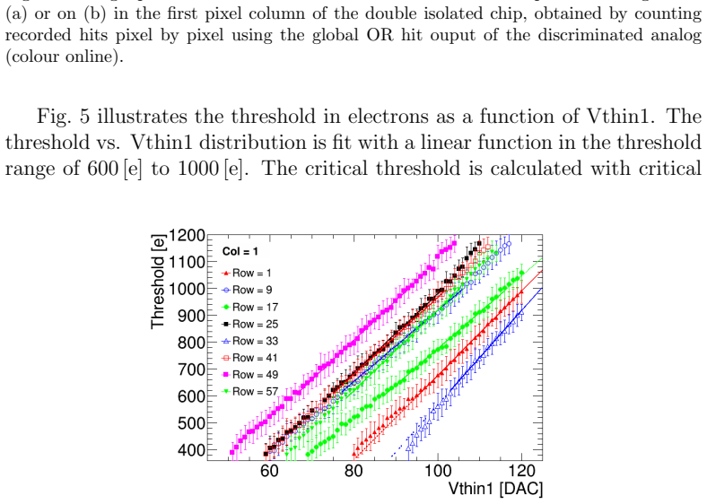
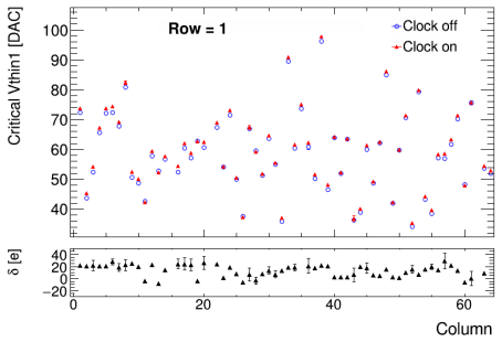
The measurement's engine is the noise-occupancy critical threshold. With a pixel's discriminator threshold swept downward, the firing rate rises exponentially, and the threshold at which the firing rate crosses 0.1 Hz serves as a sensitive proxy for the total noise; because the crossing sits roughly five noise-sigma from zero, a small threshold shift corresponds to a measurable noise change. This method avoids the bias of charge injection used in S-curve fitting. The second machinery is the current-injection path: a pad on the digital power grid at the top of the chip lets the study draw a controlled alternating current through the digital distribution network while normal supply stays at 1.2 V, producing a known digital aggressor. Comparing critical-threshold shifts with the aggressor on versus off, then normalizing by injected current amplitude, gives the per-milliamp noise transfer that separates the two isolation strategies.
What would settle it
Inject currents from about 0.6 mA to 4.8 mA into the digital power of a digital-isolated chip at 1 MHz, 18 MHz, and a frequency near the measured PSRR peak, and check whether the critical-threshold shift is proportional to current at each frequency. If the shift per milliampere is not constant for digital-isolated chips, the per-mA comparison is biased; if it is constant, the central comparison holds.
Extended reading notes
Core claim
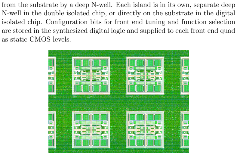
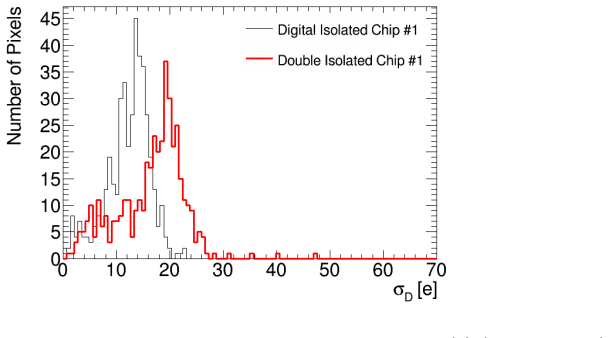
The central claim is that digital isolation is better than double isolation for the pixel readout chips tested. In measurements with a 1 MHz square-wave current of 4.8 mA and sine-wave currents from 1.2 to 2.4 mA, the average noise coupled from digital to analog, expressed as $\sigma'_D$ per mA, is lower and flatter versus frequency in the digital-isolated chips than in the double-isolated chips. The double-isolated chips also show a frequency-dependent peak in coupling that resembles the simulated ground PSRR of the front end, while the digital-isolated chips do not. The paper interprets this as evidence that the dominant coupling path is not through the substrate but through the metal stack: the double-isolated analog front end sits in a deep N-well whose ground is higher impedance than the substrate, so digital supply current can shake that local ground more easily. Since analog and digital grounds are separated on-chip to the bonding pads, the measured noise increase under injected current is attributed to this ground-shaking rather than to substrate conduction.
Load-bearing premise
The comparison assumes that digital-isolated chips respond linearly to injected current at all frequencies, even though linearity was only demonstrated for one double-isolated chip at one frequency; if the digital-isolated chips saturate or respond nonlinearly at the larger injection amplitudes, the per-milliamp normalization would favor them unfairly.
Editorial extensions
If this is right
- In 65 nm bulk CMOS pixel readout chips, fabricating analog front ends directly on the substrate can yield lower digital-to-analog noise coupling than placing them in deep N-wells.
- The double-isolated design's higher-impedance analog ground is the likely point of vulnerability, so improving the ground network of isolated analog wells may recover or exceed the digital-isolated performance.
- For normal chip operation both strategies are adequate; the practical advantage of digital isolation appears only when digital supply current fluctuates strongly.
- The correlation with front-end ground PSRR suggests that mixed-signal ground impedance, not substrate conductivity, is the key design variable for this process.
Reading between the lines
- The result likely generalizes to other mixed-signal ASICs sharing a low-resistivity substrate: tying analog ground to a large substrate node can outperform local well isolation, but the optimal strategy will still depend on substrate resistivity, package inductance, and digital current transients.
- A direct way to test the metal-stack-coupling mechanism would be to compare two digital-isolated chips with identical analog front ends but different substrate contact densities; if coupling is dominated by metal-to-well capacitance, contact density should only weakly affect noise.
- The per-mA linearity assumption, demonstrated only for one double-isolated chip, could be checked on digital-isolated chips; this is the most direct way to validate the comparison.
Signed reviews
Editorial analysis
A structured set of objections, weighed in public.
Referee Report
Summary. The manuscript reports a comparison of two substrate-isolation strategies implemented in the same 65 nm pixel readout ASIC (FE65-P2): double isolation, in which both analog and digital circuits are placed in deep N-wells, and digital isolation, in which only digital circuits are isolated and analog ground is tied to the substrate. The authors measure the shift in the critical discriminator threshold (the threshold at which the pixel noise occupancy reaches 0.1 Hz) when a controlled AC current is injected into the digital power network, convert the shift into an equivalent noise width sigma_D' using a 5-sigma relation, and compare the resulting sigma_D' per mA as a function of frequency. They find that the digital-isolated chips have lower and flatter coupling, and they suggest that the advantage arises from the lower impedance of the substrate-referenced analog ground, which is less susceptible to metal-stack coupling than the isolated well ground.
Significance. If the result holds, it is a practically valuable data point for mixed-signal ASIC design in deep submicron CMOS: it shows that, at least for this front-end architecture, tying analog ground to the substrate can outperform an isolated analog well, and it offers a plausible physical explanation via the ground PSRR. The strength of the paper is the unusual experimental opportunity—two otherwise identical chips differing only in isolation—and the use of a sensitive occupancy-based method that avoids charge-injection bias. The central comparison is empirical, not circular, and the data in Figs. 7, 10, and 12 are presented in enough detail to be re-analyzed. However, the per-mA normalization used in the main figure (Fig. 12a) rests on a linearity assumption that is not tested for the digital-isolated chips, which is the main barrier to accepting the conclusion quantitatively.
major comments (2)
- [Section 4, Fig. 12(a) and Fig. 11] The per-mA normalization of the threshold shift is load-bearing for the central claim, but its linearity basis is incomplete. The only evidence of linearity is Fig. 11, which shows delta versus injected current for one double-isolated chip at 18 MHz. The double-isolated measurements in Fig. 12(a) were taken at 1.2 mA while the digital-isolated measurements were taken at 2.4 mA, so the normalization assumes that both chip types respond linearly through the origin at all measured frequencies. If the digital-isolated chips saturate or compress at 2.4 mA, the per-mA comparison would understate their true low-current coupling and could reverse the ranking. The authors should either provide a linearity scan on a digital-isolated chip, preferably at multiple frequencies, or present the raw sigma_D' or delta values without amplitude normalization, or justify the assumption with a physical model.
- [Sections 2 and 3, conversion formulas] The conversion of the measured threshold shift delta into a noise width sigma_D depends on the assumed 5-sigma relation between the critical threshold and the noise distribution. This factor is asserted rather than measured, and it is implicitly assumed to be identical for both chip types and for all injected-current conditions. Because the final comparison is a ratio-like quantity (sigma_D' per mA) between chip types, a constant error in the 5-sigma factor would not change the ranking, but a chip-type- or frequency-dependent deviation from Gaussian behavior would. The paper would be strengthened by a direct consistency check between the S-curve width (used for sigma_A and sigma_AD) and the NOCC-derived width for the same pixel under the same conditions, or by a sensitivity scan of the conclusion under variations of the 5-sigma factor (e.g., 4.5 sigma and 5.5 sigma).
minor comments (5)
- [Section 2, last paragraph] The word 'theshold' is a typo; it should be 'threshold'. Also, the phrase 'critical theshold' appears twice and should be corrected.
- [Fig. 11 caption] The word 'critial' should be 'critical' in the caption.
- [Author list] The name 'Dario Gnanib' appears to be a typo; it should likely be 'Dario Gnani'.
- [Reference [4]] The reference 'S Helmuth, Semiconductor Detector Systems' is incorrect; the book is by Helmuth Spieler. The citation should be updated to Spieler, H., 'Semiconductor Detector Systems', Oxford University Press, 2005.
- [Section 4, first measurement paragraph] The reported injected current percentage '20.87%' has an excessive number of significant digits; given the measurement context, '20.9%' or 'about 21%' would be clearer.
Circularity Check
No circularity: the isolation comparison is an empirical measurement; the per-mA normalization rests on an unverified linearity assumption but does not reduce the conclusion to an input by construction.
full rationale
The paper's derivation chain is self-contained and empirical. The two chip types differ only by the isolation strategy, and the figure of merit is the measured increase in single-pixel noise when digital activity or injected current is present. The quantities sigma_A, sigma_{A xor D}, and sigma_D' are obtained from S-curve fits and NOCC critical-threshold shifts using the stated assumptions of Gaussian noise, a 5-sigma critical threshold, and quadrature noise addition; these are modelling assumptions used to convert measurements, not definitions that force the conclusion. The central comparison in Fig. 12(a) is a direct measurement of sigma_D' per mA, not a fitted parameter renamed as a prediction. The paper does cite prior work for the FE65-P2 design ([1], [2]) and for FE-I4B noise uniformity ([3]), but these citations are provenance or external comparison, not load-bearing support for the isolation result. One limitation is correctly visible in the text: the per-mA normalization assumes linearity of threshold shift versus injected current, demonstrated only in Fig. 11 on one double-isolated chip at 18 MHz, and extrapolated to digital-isolated chips at 2.4 mA and to all frequencies. That is a robustness concern about an experimental scaling choice, not a circularity: no equation in the paper defines the digital-isolation advantage by construction, and the measurements would stand or fall on the data even if the linearity assumption were violated. No self-definitional step, fitted-input-called-prediction step, self-citation chain, or renaming of a known result is present.
Assumptions & free parameters
free parameters (3)
- floor_occupancy =
0.1 Hz
- sigma_factor =
5
- threshold_to_vthin1_slope =
Not given numerically (Fig 5)
assumptions (3)
- domain assumption Noise is Gaussian and the zero-threshold firing rate is about 10^6 per second, so a firing rate of 0.1 Hz corresponds to a threshold about 5 standard deviations above zero.
- standard math Analog and digital noise sources are independent and add in quadrature.
- ad hoc to paper The critical threshold shift is linear in the injected current amplitude for both chip types and at all frequencies, so dividing by amplitude yields a valid per-mA comparison.
Cite this review
Pith. "Pith review of Measured Effectiveness of Deep N-well Substrate Isolation in a 65nm Pixel Readout Chip Prototype." pith.science (2026). https://pith.science/paper/ZHP2VGMV
@misc{pith2026190806182,
  author       = {Pith},
  title        = {Pith review of: Measured Effectiveness of Deep N-well Substrate Isolation in a 65nm Pixel Readout Chip Prototype},
  year         = {2026},
  howpublished = {\url{https://pith.science/paper/ZHP2VGMV}},
  note         = {Machine review of arXiv:1908.06182}
}
read the original abstract
The same charge sensitive preamplifier and discriminator circuit with different isolation strategies has been tested to compare the isolation of both analog and digital circuits from the substrate of a 65nm bulk CMOS process to the isolation of only digital circuits, tying analog ground locally to the substrate. This study will show that the circuit with analog on the substrate and digital in deep N-well has better noise isolation between analog and digital.
Figures


Figures from the paper (10 more)



Reference graph
Works this paper leans on
- [1]
-
[2]
The RD53 collaboration, Recent progress of RD53 Collaboration to- wards next generation Pixel Read-Out Chip for HL-LHC, JINST 11 (2016) C12058. 13
work page 2016
-
[3]
M Backhaus, Characterization of the FE-I4B pixel readout chip pro- duction run for the ATLAS Insertable B-layer upgrade, JINST 8 (2013) C03013
work page 2013
-
[4]
S Helmuth, Semiconductor Detector Systems, Semiconductor Science and Technology, Oxford University Press, 2005. 14
work page 2005
Reviewed August 14, 2026 · model on record in the stance chip above.
Discussion (0). Continue with ORCID to comment.