Semiconductor module
Pith reviewed 2026-05-15 18:01 UTC · model grok-4.3
The pith
A half-bridge semiconductor module places three input terminals on one side of the power elements and output terminals on the opposite side.
A machine-rendered reading of the paper's core claim, the machinery that carries it, and where it could break.
Core claim
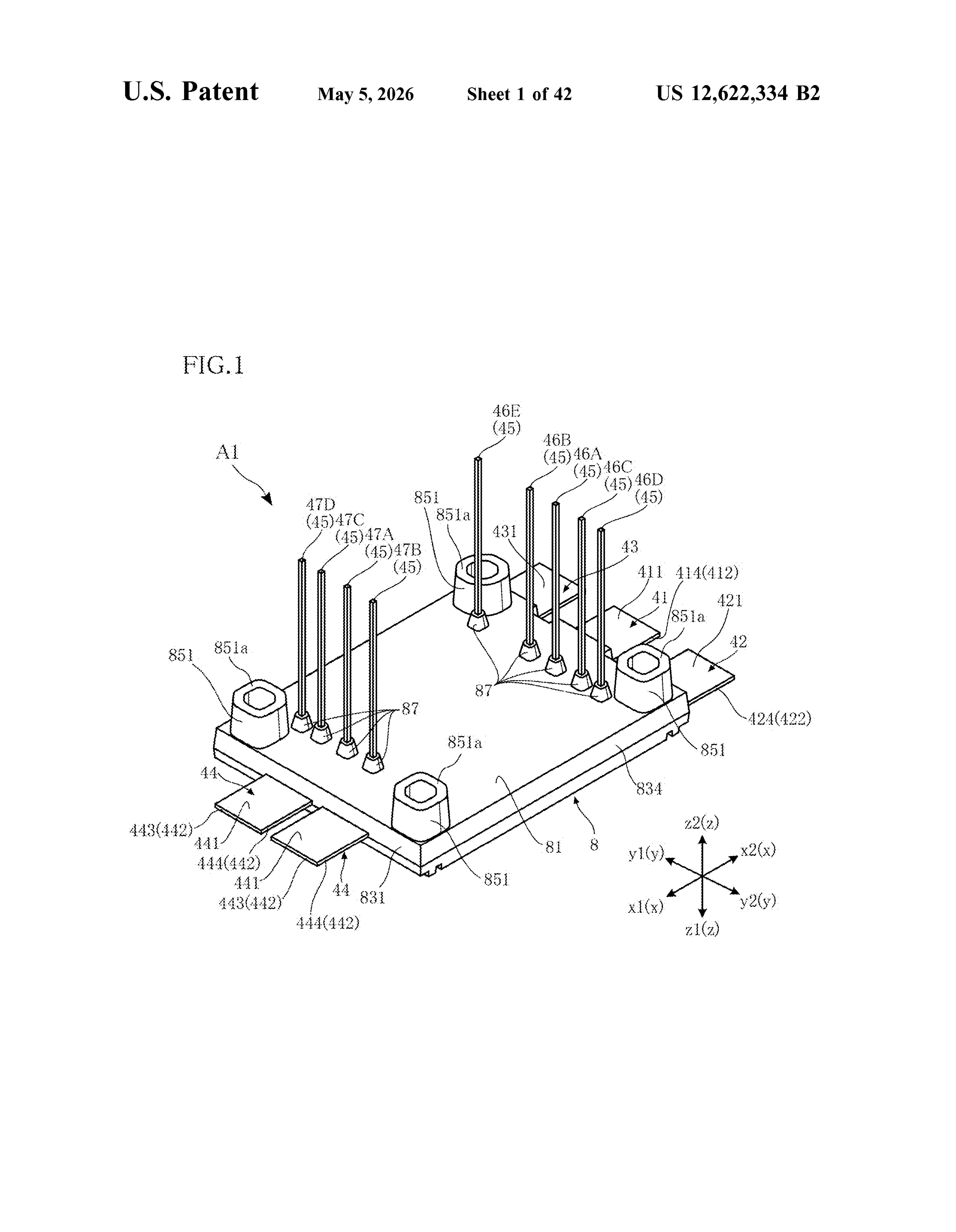
The module comprises a supporting substrate with two metal layers, two metal-plate conductive portions, two semiconductor switches forming the half-bridge arms, two wiring substrates carrying patterned metal traces, and a terminal set in which a first input terminal is flanked by second and third input terminals on one side of the device while output terminals occupy the opposite side.
What carries the argument
The front-to-back terminal split across the half-bridge elements, with the three input terminals grouped on one side and the output terminal(s) on the other, carried by the two metal-plate conductive portions and the overlying patterned wiring substrates.
Load-bearing premise
The specific front-to-back terminal arrangement will produce the intended current paths and isolation without further electrical measurements or simulations.
What would settle it
A prototype built to the described dimensions that shows longer current-loop inductance or higher voltage overshoot than a conventional side-by-side terminal layout under the same switching test.
Figures
read the original abstract
1 . A semiconductor module provided with a half-bridge circuit, the semiconductor module comprising: a supporting substrate including a first insulating layer, a first metal layer and a second metal layer; a first conductive portion and a second conductive portion both bonded to the supporting substrate and made of a metal plate member; a first semiconductor element and a second semiconductor element constituting an upper arm circuit and a lower arm circuit, respectively, in the half-bridge circuit and both having a switching function; a first wiring substrate and a second wiring substrate each including a second insulating layer and a third metal layer formed on an upper surface of the second insulating layer, the third metal layer including a plurality of wiring portions spaced apart and insulated from each other, the first wiring substrate being disposed on the first conductive portion and electrically connected to the first semiconductor element, the second wiring substrate being disposed on the second conductive portion and electrically connected to the second semiconductor element; a first input terminal disposed on one side of a first direction perpendicular to a thickness direction relative to the first semiconductor element and the first conductive portion; a second input terminal and a third input terminal both disposed on the one side of the first direction relative to the first semiconductor element and the first conductive portion, the second input terminal and the third input terminal being opposite from each other with the first input terminal sandwiched therebetween in a second direction perpendicular to the thickness direction and the first direction; at least one output terminal disposed on another side of the first direction relative to the second sem
Editorial analysis
A structured set of objections, weighed in public.
Referee Report
Summary. The manuscript claims a semiconductor module implementing a half-bridge circuit via a supporting substrate with first and second metal layers, first and second metal-plate conductive portions, upper- and lower-arm semiconductor switching elements, two wiring substrates each carrying spaced third-metal-layer wiring portions, and a terminal layout in which three input terminals lie on one side of the first direction (with the second and third inputs flanking the first) while at least one output terminal lies on the opposite side.
Significance. If the described geometry is enabling, the arrangement supplies a concrete, manufacturable half-bridge power-module topology that places input and output terminals on opposing sides of the substrate stack; this configuration is potentially useful for compact inverter layouts, though the filing supplies no inductance, thermal, or comparative data to quantify any performance gain.
minor comments (2)
- [Abstract] The abstract is truncated mid-sentence after 'the second sem'; the full claim language should be supplied in a revised version for completeness.
- [Description] The description repeatedly refers to 'one side of the first direction' and 'another side' without an accompanying figure label or coordinate diagram; adding an explicit top-view schematic with labeled axes would improve clarity of the terminal placement.
Simulated Author's Rebuttal
We thank the referee for the careful reading of the manuscript and for the positive recommendation to accept. The report accurately captures the core geometric arrangement of the half-bridge module.
Circularity Check
No significant circularity
full rationale
The document is a utility patent whose sole content is a structural description of a half-bridge semiconductor module geometry (supporting substrate, metal plates, dual wiring substrates, and terminal placement). No equations, fitted parameters, predictions, or derivations appear anywhere in the text; the claim is the enablement of the physical arrangement itself. Consequently no step reduces to a self-definition, fitted input, or self-citation chain.
Axiom & Free-Parameter Ledger
Lean theorems connected to this paper
-
IndisputableMonolith.Foundation.RealityFromDistinctionreality_from_one_distinction unclear?
unclearRelation between the paper passage and the cited Recognition theorem.
A semiconductor module provided with a half-bridge circuit, the semiconductor module comprising: a supporting substrate including a first insulating layer, a first metal layer and a second metal layer; a first conductive portion and a second conductive portion both bonded to the supporting substrate and made of a metal plate member; a first semiconductor element and a second semiconductor element constituting an upper arm circuit and a lower arm circuit, respectively, in the half-bridge circuit and both having a switching function; a first wiring substrate and a second wiring substrate each...
What do these tags mean?
- matches
- The paper's claim is directly supported by a theorem in the formal canon.
- supports
- The theorem supports part of the paper's argument, but the paper may add assumptions or extra steps.
- extends
- The paper goes beyond the formal theorem; the theorem is a base layer rather than the whole result.
- uses
- The paper appears to rely on the theorem as machinery.
- contradicts
- The paper's claim conflicts with a theorem or certificate in the canon.
- unclear
- Pith found a possible connection, but the passage is too broad, indirect, or ambiguous to say the theorem truly supports the claim.
discussion (0)
Sign in with ORCID, Apple, or X to comment. Anyone can read and Pith papers without signing in.