REVIEW 2 major objections 5 minor 14 references
Correcting impedance measurements for background parasitics to characterize circuit components in cryogenic environments
T0 review · 2 major / 5 minor · reviewed 2026-08-07 · deepseek-v4-flash
Pith's one-line read Using in situ open and short calibration channels, the paper corrects two-wire LCR meter readings with $Z_x = (Z_m - Z_{Sh})/(1 - Z_m/Z_{Op})$, recovering isolated component impedances in a cryostat and extending a meter rated at 10–20 MΩ…
desk verdict Useful cryogenic component data and a standard open/short correction, but the abstract oversells the 10 pF result and the Yp=Yo closure needs a sensitivity bound. read the letter →
The pith
A machine-rendered reading of the paper's core claim, the machinery that carries it, and where it could break.
The reading
What carries the argument
The engine of the paper is the formula $Z_x = (Z_m - Z_{Sh})/(1 - Z_m/Z_{Op})$, a pointwise impedance de-embedding that comes from a lumped-element model of the measurement chain with a series parasitic impedance $Z_s$ and parallel parasitic admittances $Y_o$ and $Y_p$. The model sets $Y_p = Y_o$ so that no free parameters enter, and the open and short calibration channels supply the needed reference values at the same temperature as the component under test. Applied frequency by frequency, the formula converts raw, parasitics-dominated readings into the isolated component impedance, from which capacitance and resistance are read directly.
What would settle it
A direct check would be to measure the parasitic admittance of the BNC cable path alone and the parasitic admittance of an open PCB channel alone at the same temperature, then compare them; any difference beyond the meter's accuracy means Eq. 7 carries a bias. A second check is already in the data: a nominally $10\,\mathrm{pF}$ reference capacitor reconstructs as $3.1\text{–}3.7\,\mathrm{pF}$, so measuring the same component with an independent four-wire bridge or a known-good reference would settle whether the model's pF-scale offset is real.
Extended reading notes
Core claim
The central discovery is an algebraic de-embedding identity: if $Z_{Sh}$, $Z_{Op}$, and $Z_m$ are the measured impedances with the channel shorted, left open, and loaded by the component, then the isolated component impedance is $Z_x = (Z_m - Z_{Sh})/(1 - Z_m/Z_{Op})$. The paper applies this identity to raw two-wire LCR meter sweeps after interpolating each channel to a common frequency grid, then reads capacitance from $C_x = -1/(2\pi f\,\mathrm{Im}(Z_x))$ and resistance from $R_x = \mathrm{Re}(Z_x)$. The load-bearing demonstration is that this procedure yields frequency-stable component values across a wide range: stable pF-scale capacitors, $100\,\mathrm{M}\Omega$ resistors whose cryogenic values rise by up to an order of magnitude, and a $22\,\mu\mathrm{F}$ 5XR capacitor that collapses to roughly $940\,\mathrm{nF}$ at $360\,\mathrm{mK}$. Because the parasitics reduce the impedance seen by the meter, the transform also extends the meter's useful range beyond its manufacturer-quoted $10$–$20\,\mathrm{M}\Omega$ limits.
Load-bearing premise
The model assumes, without separately measuring it, that the parasitic effect of the two BNC cables is exactly the same as the parasitic effect of the PCB open calibration channel; if the two differ, every corrected capacitance and resistance value shifts by an amount this paper does not quantify.
Editorial extensions
If this is right
- For the two $22\,\mu\mathrm{F}$ 5XR capacitors tested, the corrected cold capacitance is about $940\text{–}950\,\mathrm{nF}$ at $360\,\mathrm{mK}$, so filter designs using these parts should be based on the measured cold value rather than the nominal one.
- A $100\,\mathrm{M}\Omega$ thick-film resistor cooled to $360\,\mathrm{mK}$ can present more than $300\,\mathrm{M}\Omega$ of low-frequency resistance, with the strongest temperature response in the parts carrying the largest rated temperature coefficient.
- The same open/short correction can be reused for any passive component mounted on the board, since it works at every frequency independently and does not require a model of the component itself.
- For resistor characterization, the frequency dependence of the corrected impedance exposes self-capacitance values—around $5\,\mathrm{pF}$ for the $100\,\mathrm{M}\Omega$ devices tested—which matters for filtering at high frequencies.
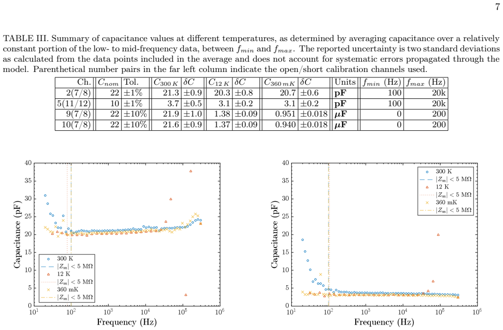
- The technique's remaining systematic limitation shows up at the pF scale: a nominally $10\,\mathrm{pF}$ capacitor reconstructed as $3.1\text{–}3.7\,\mathrm{pF}$, so pF-level results need independent verification before being used in designs.
Reading between the lines
- The same algebraic correction should transfer to any fixed two-wire fixture—room-temperature probe stations, wired test sockets, or other cryostats—as long as open and short references are measured in the same geometrical configuration, giving a general low-cost de-embedding recipe.
- One testable extension is to bound the $Y_p = Y_o$ assumption directly by adding known capacitances to the cable side of the circuit and measuring how the reconstructed $Z_x$ shifts; the paper gives no sensitivity bound for this mismatch.
- The factor-of-twenty capacitance collapse seen in high-$\kappa$ multilayer ceramic capacitors suggests that sub-Kelvin amplifier filters should favor low-$\kappa$ film capacitors, whose values changed by only a few percent in this test.
- Because the method yields complex $Z_x$ over frequency, it could populate a database of temperature-dependent self-capacitance and leakage resistance for many components, which would make cryogenic SPICE simulations far more realistic.
Signed reviews
Editorial analysis
A structured set of objections, weighed in public.
Referee Report
Summary. The paper presents a two-wire LCR meter method for measuring the complex impedance of passive components mounted in a cryostat, with in situ open/short calibration channels used to correct for wiring and PCB parasitics. The central analytical result is Eq. (7), which transforms raw meter readings Z_m, Z_op, and Z_sh into a corrected component impedance Z_x. This formula is derived under the explicit approximation that the BNC cable shunt admittance Y_p equals the PCB open-channel admittance Y_o. The method is applied to 22 µF 5XR multilayer ceramic capacitors, 22 pF and 10 pF thin-film capacitors, and 100 MΩ thick-film resistors at 300 K, 12 K, and 360 mK. The authors report a ~20x drop in capacitance for the 22 µF capacitors at low temperature, resistance increases by factors of 3–10 for the 100 MΩ resistors, and a 10 pF capacitor that measures as 3.1–3.7 pF rather than its nominal value. The paper claims the method extends the useful range of a commercial LCR meter beyond its manufacturer-specified impedance limits.
Significance. If the method is validated, it offers a simple and inexpensive route to cryogenic component characterization, which is useful for detector development in the low-temperature community. The reported 20x capacitance suppression in 5XR MLCCs is a concrete, practically important finding that is consistent with prior literature on high-κ dielectric capacitors. The paper is transparent about several limitations: the statistical uncertainties do not include systematic errors, the 10 pF result is explicitly acknowledged as a model limitation, and the Y_p = Y_o assumption is stated rather than hidden. The 300 K agreement with manufacturer nominals for the 22 pF capacitor (21.3 pF) and the 100 MΩ resistors (93–101 MΩ) provides a useful partial validation that the algebra and implementation are not grossly wrong. However, the central claim of extending meter accuracy beyond specification depends on an unquantified model assumption, and the cold-regime results are not independently anchored.
major comments (2)
- [§IV.C, Table III, Ch. 5] The derivation of Eq. (7) is algebraically consistent only under the explicit assumption Y_p = Y_o, but this assumption is neither measured nor bounded. The two admittances are physically distinct: Y_p arises from two BNC cables connecting the meter to the breakout box, while Y_o is the PCB open-channel admittance. If Y_p ≠ Y_o, Eq. (7) does not recover Z_x. For example, in a simple model with Y_p = 1, Y_o = 2, Z_s = 1, and Z_x = 2, applying the formula gives 3 instead of 2, a 50% error. Because no measurement constrains the ratio Y_p/Y_o, all quantities derived through Eq. (7)—including the Table IV cold resistance values, the pF-scale capacitance values, and the ~5 pF self-capacitance estimate in Fig. 13—carry an unquantified systematic bias. The authors should provide a sensitivity analysis that varies Y_p/Y_o over a physically plausible range (or directly measure Y_p with a dedicated open measurement at the BNC connection) and shows how C_x and R_x shift at 12 K and 360 mK. This is load-bearing because the claim of extending LCR meter accuracy beyond specification relies on Eq. (7) being quantitatively reliable in the cold, high-impedance regime.
- [§IV.C, Table III] The nominally 10 pF capacitor on Ch. 5 is reported as 3.1–3.7 pF at all temperatures, a large deviation from the 1% nominal value. The authors acknowledge this discrepancy and state that the model may not be accurate at such low capacitance. However, the abstract and conclusions claim that the procedure was used to 'successfully measure 10 pF' capacitors. This is internally inconsistent: a 3.1–3.7 pF reading for a 10 pF certified component is not a successful measurement unless a quantitative explanation or calibration factor is provided. The authors should either reframe the claim, or provide a model-based estimate of the systematic offset at pF levels (for example, a residual shunt capacitance or a small Y_p/Y_o mismatch that produces a baseline error). Without this, the 10 pF result actually weakens the central claim that the method extends meter accuracy.
minor comments (5)
- [§II] There are several typos in this section: 'seprately' should be 'separately', 'sort' should be 'short' in the phrase 'open, sort measurements', and 'ω = 2π x sampling frequency' should use a multiplication symbol or specify the sampling frequency variable.
- [§IV.A] In the discussion of Fig. 5, the text refers to '12 K and 360 K data'; the latter should be '360 mK data' for consistency with the rest of the paper.
- [§IV.C] The word 'dyring' in 'successful component isolation dyring the analysis' should be 'during'.
- [§IV.D] The semicircle fit for the 360 mK Ch. 6 data uses R_o = 560 MΩ, whereas Table IV lists R_360mK = 480 ± 120 MΩ. The text does not explain why the fit value differs from the tabulated value; this may confuse readers who compare the figure with the table.
- [Table III] For channels 9 and 10, the averaging range is listed as '0 200' Hz. Since the LCR meter starts at 20 Hz and a 0 Hz lower bound is not physical, this entry should be clarified (e.g., whether the lower limit was actually 20 Hz or a lower-frequency subset).
Circularity Check
No significant circularity: Eq. 7 is an algebraic open/short correction with no free parameters, validated against independent manufacturer values at 300 K; the unverified Yp=Yo closure assumption is a systematic-bias limitation, not a circular step.
full rationale
The paper's central correction, Eq. 7 (Zx = (Zm - ZSh)/(1 - Zm/ZOp)), is derived algebraically from Eqs. 4-6 using the pi-model after the explicit closure assumption 'Yp = Yo' (Sec. III). No parameter is fitted to any target output: ZSh, ZOp, and Zm are all measured quantities from dedicated open/short channels and device channels, and the corrected Cx, Rx, and self-capacitance values are deterministic outputs of Eq. 7, not inputs that are renamed as predictions. The model is externally anchored: the 300 K results agree with independent manufacturer nominal values (21.3 pF vs. 22 pF for Ch. 2; 21.6-21.9 uF vs. 22 uF for Chs. 9/10; all four 100 MOhm resistors within roughly 2-7% of nominal), so the method is not self-validating. The weakest assumption, that the BNC-cable parallel admittance Yp equals the PCB open-channel admittance Yo, is a genuine closure approximation that would systematically bias extracted values if violated, and the paper provides no sensitivity bound; the paper also concedes its own limits at 10 pF ('the 10 pF capacitor results should be taken as an indication that further scrutiny of the finer details of this circuit correction model is necessary') and that the tabulated uncertainties 'do not account for systematic errors propagated through the model' (Tables III-IV). However, an unverified or even incorrect assumption is a correctness risk, not circularity: Eq. 7 does not reduce to its inputs by construction, and the Yp=Yo equality is not a definition of one quantity in terms of the other. The only author-overlapping citation is [4] (Anczarski et al.), used for context and motivation (SPLENDOR amplifier design and its elevated noise), not to justify the correction formula or the physical conclusions. The graphical selection of averaging frequency windows (Sec. IV.C) and the post hoc identification of the 60 Hz phase offset without implementing a correction (Sec. IV.A) are analysis choices and honest reporting, not fitted inputs masquerading as predictions. Overall, the derivation chain is self-contained, free of load-bearing self-citations, and externally benchmarked, so no circular step is present.
Assumptions & free parameters
free parameters (2)
- Frequency averaging windows (fmin, fmax) per component =
22 uF: (0, 200) Hz; 22 pF: (100 Hz, 20 kHz); 10 pF: (100 Hz, 20 kHz); resistors: f < 50-100 Hz
- Fit value Ro for the 360 mK Ch. 6 impedance semicircle =
560 MOhm
assumptions (4)
- ad hoc to paper Yp = Yo, i.e., the BNC cable parallel admittance equals the PCB open-channel admittance
- domain assumption A pi-network with Yp in parallel, Zs in series, and Yo in parallel captures the full parasitic environment
- domain assumption A nearby open/short calibration channel has the same parasitics as each test channel
- domain assumption The single LCR meter calibration performed per cool-down remains valid at all temperatures
Cite this review
Pith. "Pith review of Correcting impedance measurements for background parasitics to characterize circuit components in cryogenic environments." pith.science (2026). https://pith.science/paper/5IOAAFQ3
@misc{pith2026250612268,
  author       = {Pith},
  title        = {Pith review of: Correcting impedance measurements for background parasitics to characterize circuit components in cryogenic environments},
  year         = {2026},
  howpublished = {\url{https://pith.science/paper/5IOAAFQ3}},
  note         = {Machine review of arXiv:2506.12268}
}
read the original abstract
Predictable circuit response is a critical prerequisite for accurate electronic measurements. We describe a powerful, yet straightforward, experimental method and analysis model that utilizes an affordable LCR meter in conjunction with an in situ parasitic impedance background correction procedure to measure the temperature-dependent impedance (magnitude and phase) of individual passive circuit elements mounted in a cryostat. We show how the model unambiguously identified a 20x drop in capacitance for 22 microF 5XR multilayer ceramic capacitors cooled from 300 K to 360 mK in an environment with parasitic capacitance of order 300 pF. The same experimental procedure, based on a simple two-wire measurement, was also used to successfully measure 10 pF and 22 pF thin-film capacitors and 100 MOhm thick-film resistors. The results showed that the resistor values increased by up to an order of magnitude when the devices were cooled from 300 K to 360 mK. Most importantly, the simple data acquisition method and robust analysis model were shown to effectively extend the accuracy of a simple benchtop LCR meter beyond its manufacturer-guaranteed values for a wide range of measurement frequencies.
Figures


Figures from the paper (10 more)




Reference graph
Works this paper leans on
- [1]
- [2]
- [3]
-
[4]
Anczarski, et.al, J Low Temp Phys 214, 256-262 (2024)
J. Anczarski, et.al, J Low Temp Phys 214, 256-262 (2024)
work page 2024
-
[5]
B&K Precision 300 kHz Bench LCR Meter User Manual , B&K Precision Corporation, Yorba Linda, CA, (2015)
work page 2015
-
[6]
Kalbitz, Wurth Elektronik, Appl
R. Kalbitz, Wurth Elektronik, Appl. Note 109a [www.we- online.com], (2022)
work page 2022
-
[7]
Lee, et.al, J Korean Ceram Soc 49, 475-483 (2012)
J.S. Lee, et.al, J Korean Ceram Soc 49, 475-483 (2012)
work page 2012
-
[8]
Design techniques for a stable operation of cryogenic field- programmable gate arrays
H. Homulle, S. Visser, B. Patra and E. Charbon,“Design techniques for a stable operation of cryogenic field- programmable gate arrays”,Rev. Sci. Instrum. 89, no.1, (2018)
work page 2018
Show all 14 references
-
[9]
Teyssandier and D
F. Teyssandier and D. Prêle,Ninth International Work- shop on Low Temperature Electronics , (2010)
2010
-
[10]
Pan,Cryogenics 45, 463-467 (2005)
M.-J. Pan,Cryogenics 45, 463-467 (2005)
2005
-
[11]
open” chan- nels (no component installed) and two others (Chs 8, 12) were selected as “short
on the sample PCB were designated as “open” chan- nels (no component installed) and two others (Chs 8, 12) were selected as “short” channels, where a 0Ω resistor was mounted in place of a test component. Using data from these two channels in combination with thein situ meter c...
-
[12]
Novikov, D
I. Novikov, D. Volkhin and A. Vostretsov,IEEE 3rd In- ternational Conference on Problems of Informatics, Elec- tronics and Radio Engineering pp. 300-304, (2024)
2024
-
[13]
Accu-P Series Thin-Film RF/Microwave Capacitor Technology, Kyocera AVX, [datasheet] TDS-RFM-0032
-
[14]
Teverovsky,IEEE Trans
A. Teverovsky,IEEE Trans. on Components, Packaging and Manufacturing Technology 4, 1169-1176, (2014)
2014
Reviewed August 7, 2026 · model on record in the stance chip above.
Discussion (0). Continue with ORCID to comment.