End-to-End Physical Design Automation Flow for Yield-Optimized Inverse-Designed Large-Scale Electronic-Photonic Integrated Circuits
Pith reviewed 2026-05-10 09:44 UTC · model grok-4.3
The pith
OptoSynthesizer creates fabrication-ready layouts for large-scale electronic-photonic chips by chaining inverse design, placement, and routing with yield optimization.
A machine-rendered reading of the paper's core claim, the machinery that carries it, and where it could break.
Core claim
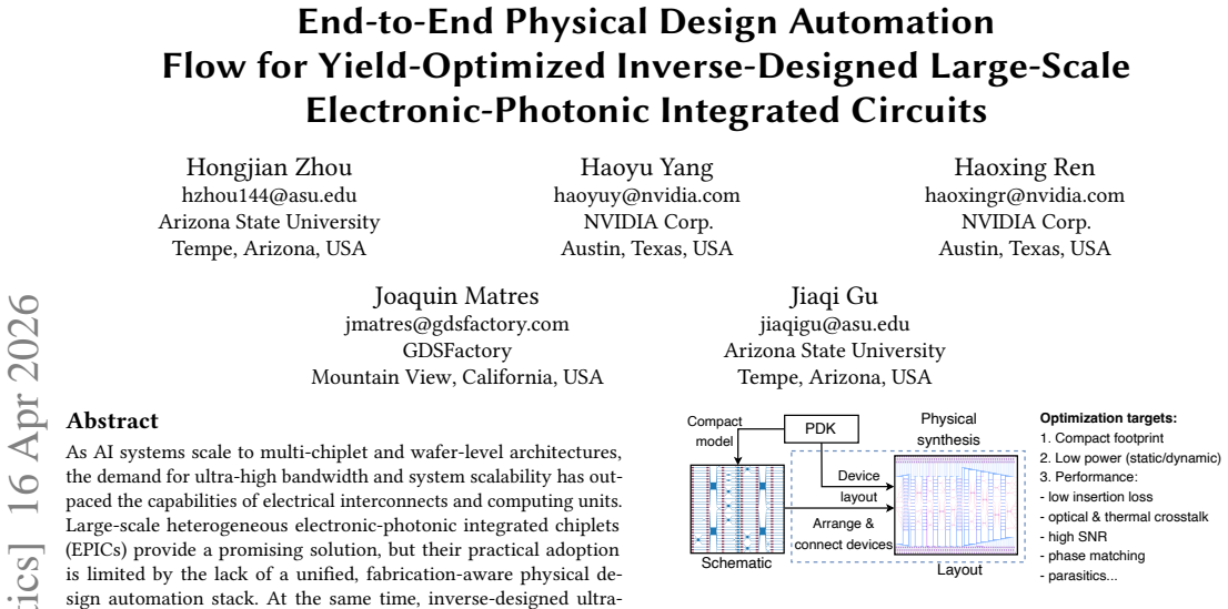
OptoSynthesizer integrates OptoSynthesizer-InvDes for physical-AI-augmented, digital-twin-assisted photonic inverse design and inverse lithography, OptoSynthesizer-Place for GPU-accelerated routing-informed EPIC placement, and OptoSynthesizer-Route for hierarchical curvy-aware waveguide routing with global-planning-assisted electrical-optical co-routing, thereby forming a seamless pipeline from EPIC netlists to fabrication-ready, yield-robust GDS layouts that enable compact large-scale photonic tensor cores and high-bandwidth interconnect fabrics for heterogeneous EPIC platforms.
What carries the argument
The OptoSynthesizer flow, which chains inverse design, routability-optimized placement, and curvy waveguide co-routing to produce yield-robust layouts directly from netlists.
If this is right
- Compact large-scale photonic tensor cores become feasible for AI computing.
- High-bandwidth interconnect fabrics support multi-chiplet and wafer-level architectures.
- Designers obtain fabrication-ready GDS layouts directly from EPIC netlists without fragmented manual steps.
- Inverse-designed photonic devices gain practical design-for-manufacturing support at scale.
Where Pith is reading between the lines
- The GPU-accelerated placement step implies the flow can scale to circuits far larger than current manual methods allow.
- Embedding yield optimization early may reduce the number of design iterations needed before tape-out.
- The co-routing of optical and electrical signals could implicitly lower crosstalk in dense layouts, though this is not quantified.
- Similar automation pipelines might later be extended to other hybrid technologies once the EPIC case is demonstrated.
Load-bearing premise
The three toolkits integrate without major interface problems or added yield losses, and the generated layouts actually achieve real manufacturing yield targets in silicon photonics processes.
What would settle it
Fabrication and yield measurement of a large-scale photonic tensor core or interconnect fabric produced by the full OptoSynthesizer flow, compared against the flow's predicted yield.
Figures



read the original abstract
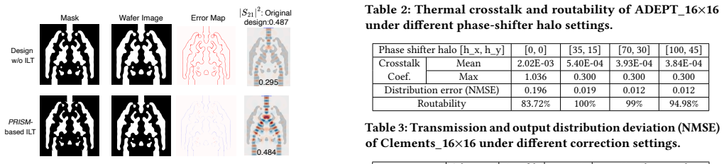
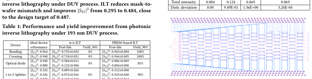
As AI systems scale to multi-chiplet and wafer-level architectures, the demand for ultra-high bandwidth and system scalability has outpaced the capabilities of electrical interconnects and computing units. Large-scale heterogeneous electronic-photonic integrated chiplets (EPICs) provide a promising solution, but their practical adoption is limited by the lack of a unified, fabrication-aware physical design automation stack. At the same time, inverse-designed ultra-compact photonic devices offer orders-of-magnitude improvements in spatial and spectral density, yet remain constrained by insufficient design-for-manufacturing support and yield optimization. In this work, we present OptoSynthesizer, an end-to-end physical design automation flow for yield-optimized, inverse-designed EPICs. It integrates three key components across the physical design pipeline: (1) OptoSynthesizer-InvDes, a physical-AI-augmented, digital-twin-assisted photonic inverse design and photonics-aware inverse lithography framework; (2) OptoSynthesizer-Place, a GPU-accelerated routing-informed EPIC placer for large-scale routability-optimized layout; and (3) OptoSynthesizer-Route, a hierarchical curvy-aware waveguide router with global-planning-assisted electrical-optical co-routing. Together, these toolkits form a seamless flow from EPIC netlists to fabrication-ready, yield-robust GDS layouts. We demonstrate how this framework enables compact large-scale photonic tensor cores and high-bandwidth interconnect fabrics for heterogeneous EPIC platforms, providing a practical foundation for manufacturable large-scale EPICs in next-generation AI systems.
Editorial analysis
A structured set of objections, weighed in public.
Referee Report
Summary. The paper presents OptoSynthesizer, an end-to-end physical design automation flow for yield-optimized inverse-designed large-scale electronic-photonic integrated circuits (EPICs). It integrates three components: OptoSynthesizer-InvDes (physical-AI-augmented, digital-twin-assisted inverse design and photonics-aware inverse lithography), OptoSynthesizer-Place (GPU-accelerated, routing-informed placer for routability-optimized EPIC layouts), and OptoSynthesizer-Route (hierarchical curvy-aware waveguide router with global-planning-assisted electrical-optical co-routing). The flow claims to convert EPIC netlists into fabrication-ready, yield-robust GDS layouts, enabling compact photonic tensor cores and high-bandwidth interconnect fabrics.
Significance. If the integration and yield claims are substantiated with quantitative data, the work could provide a practical automation foundation for manufacturable large-scale heterogeneous EPICs, addressing scalability limits in AI hardware. The combination of inverse design with placement and routing under a yield-aware digital-twin approach represents a potentially valuable systems-level contribution, but the current manuscript supplies no benchmarks, yield numbers, or silicon results to assess this.
major comments (2)
- Abstract: The central claim that the integrated flow produces 'yield-robust GDS layouts' that 'meet manufacturing yield targets' rests on unvalidated assertions about 'physical-AI-augmented, digital-twin-assisted' methods and 'yield-optimized' routing. No quantitative yield metrics, process-variation simulations, mask-error analysis, or measured silicon results are provided to support this, making the claim unevaluable from the manuscript.
- Abstract: No evidence or interface specifications are given for how OptoSynthesizer-InvDes, -Place, and -Route combine without introducing yield-loss problems at boundaries (e.g., waveguide discontinuities or placement-induced routing congestion), which is load-bearing for the 'seamless flow' and 'fabrication-ready' assertions.
minor comments (1)
- Abstract: The dense use of compound names (OptoSynthesizer-InvDes etc.) and claims without a high-level block diagram or performance delta table reduces immediate readability; adding one would clarify the pipeline.
Simulated Author's Rebuttal
We thank the referee for the constructive comments on our manuscript. We address the major concerns point by point below and will make revisions to improve the substantiation of our claims.
read point-by-point responses
-
Referee: Abstract: The central claim that the integrated flow produces 'yield-robust GDS layouts' that 'meet manufacturing yield targets' rests on unvalidated assertions about 'physical-AI-augmented, digital-twin-assisted' methods and 'yield-optimized' routing. No quantitative yield metrics, process-variation simulations, mask-error analysis, or measured silicon results are provided to support this, making the claim unevaluable from the manuscript.
Authors: We agree that the abstract's yield-robust claims would benefit from quantitative backing to be fully evaluable. The manuscript describes the mechanisms for yield optimization, including digital-twin-assisted variation modeling in inverse design and congestion-aware placement/routing. In revision, we will incorporate process-variation simulations, estimated yield metrics, and mask-error analysis derived from the framework. Measured silicon results are not available, as this work focuses on the design automation methodology rather than fabricated devices; we will explicitly note this scope limitation. revision: partial
-
Referee: Abstract: No evidence or interface specifications are given for how OptoSynthesizer-InvDes, -Place, and -Route combine without introducing yield-loss problems at boundaries (e.g., waveguide discontinuities or placement-induced routing congestion), which is load-bearing for the 'seamless flow' and 'fabrication-ready' assertions.
Authors: We acknowledge the need for clearer evidence on component integration to support the seamless-flow claims. The full manuscript outlines the data interfaces and co-optimization strategies, such as routing-informed placement constraints and curvy-aware waveguide continuity checks. To directly address potential boundary issues, we will expand the relevant sections with detailed interface specifications, additional figures illustrating boundary handling, and analysis demonstrating mitigation of discontinuities and congestion in the revised manuscript. revision: yes
- Measured silicon results, which are outside the scope of this design-automation-focused manuscript.
Circularity Check
No circularity: engineering framework description without derivations or fitted predictions
full rationale
The paper presents an integrated physical design flow (OptoSynthesizer) composed of three toolkits for EPIC layout generation. No equations, parameter fits, uniqueness theorems, or predictive claims that reduce to inputs appear in the abstract or framework description. Central assertions concern tool integration and enabling compact layouts, which are engineering statements rather than mathematical derivations. No self-citations, ansatzes, or renamings of known results are load-bearing. The absence of any derivation chain means no opportunity for circular reduction exists; the contribution is self-contained as a systems paper.
Axiom & Free-Parameter Ledger
Reference graph
Works this paper leans on
-
[1]
Universal photonic artificial intelligence acceleration.Nature, 640(8058):368–374, 2025
Sufi R Ahmed, Reza Baghdadi, Mikhail Bernadskiy, Nate Bowman, Ryan Braid, Jim Carr, Chen Chen, Pietro Ciccarella, Matthew Cole, John Cooke, et al. Universal photonic artificial intelligence acceleration.Nature, 640(8058):368–374, 2025
work page 2025
-
[2]
Hailong Zhou, Jianji Dong, Junwei Cheng, Wenchan Dong, Chaoran Huang, Yichen Shen, Qiming Zhang, Min Gu, Chao Qian, Hongsheng Chen, et al. Photonic ma- trix multiplication lights up photonic accelerator and beyond.Light: Science & Applications, 11(1):30, 2022
work page 2022
-
[3]
Popstar: A robust modular optical noc architecture for chiplet- based 3d integrated systems
Yvain Thonnart, Stéphane Bernabé, Jean Charbonnier, Christian Bernard, David Co- riat, César Fuguet, Pierre Tissier, Benoît Charbonnier, Stéphane Malhouitre, Damien Saint-Patrice, et al. Popstar: A robust modular optical noc architecture for chiplet- based 3d integrated systems. InDATE 2020-Design, Automation & Test in Europe Conference & Exhibition, page...
work page 2020
-
[4]
Momchil Minkov, Ian AD Williamson, Lucio C Andreani, Dario Gerace, Beicheng Lou, Alex Y Song, Tyler W Hughes, and Shanhui Fan. Inverse design of photonic crystals through automatic differentiation.Acs Photonics, 7(7):1729–1741, 2020
work page 2020
-
[5]
Hongjian Zhou, Pingchuan Ma, and Jiaqi Gu. Toward intelligent electronic-photonic design automation for large-scale photonic integrated circuits: from device inverse design to physical layout generation. InOptical Design Automation, volume 13601, pages 69–78. SPIE, 2025
work page 2025
-
[6]
Joaquin Matres et al. Gdsfactory. https://github.com/gdsfactory/gdsfactory, 2024
work page 2024
-
[7]
Erfan Khoram, Xiaoping Qian, Ming Yuan, and Zongfu Yu. Controlling the minimal feature sizes in adjoint optimization of nanophotonic devices using b-spline surfaces. Optics Express, 28(5):7060–7069, 2020
work page 2020
-
[8]
Hongjian Zhou, Haoyu Yang, Nicholas Gangi, Tianle Xu, Rena Huang, and Jiaqi Gu. PRISM: Photonics-Informed Inverse Lithography for Manufacturable Inverse- Designed Photonic Integrated Circuits.arXiv preprint arXiv:2602.15762, 2026
-
[9]
Robust design of topology-optimized metasurfaces.Optical Materials Express, 9(2):469–482, 2019
Evan W Wang, David Sell, Thaibao Phan, and Jonathan A Fan. Robust design of topology-optimized metasurfaces.Optical Materials Express, 9(2):469–482, 2019
work page 2019
-
[10]
Fengwen Wang, Jakob S Jensen, and Ole Sigmund. Robust topology optimization of photonic crystal waveguides with tailored dispersion properties.Journal of the Optical Society of America B, 28(3):387–397, 2011
work page 2011
-
[11]
Mattias Schevenels, Boyan Stefanov Lazarov, and Ole Sigmund. Robust topology optimization accounting for spatially varying manufacturing errors.Computer Methods in Applied Mechanics and Engineering, 200(49-52):3613–3627, 2011
work page 2011
-
[12]
Erez Gershnabel, Mingkun Chen, Chenkai Mao, Evan W Wang, Philippe Lalanne, and Jonathan A Fan. Reparameterization approach to gradient-based inverse design of three-dimensional nanophotonic devices.ACS Photonics, 10(4):815–823, 2022
work page 2022
-
[13]
Cambridge University Press, 2015
Lukas Chrostowski and Michael Hochberg.Silicon photonics design: from devices to systems. Cambridge University Press, 2015
work page 2015
-
[14]
Yu-Kai Chuang, Kuan-Jung Chen, Kun-Lin Lin, Shao-Yun Fang, Bing Li, and Ulf Schlichtmann. Planaronoc: concurrent placement and routing considering crossing minimization for optical networks-on-chip. InProceedings of the 55th Annual Design Automation Conference, pages 1–6, 2018
work page 2018
-
[15]
O-router: an optical routing framework for low power on-chip silicon nano-photonic integration
Duo Ding, Yilin Zhang, Haiyu Huang, Ray T Chen, and David Z Pan. O-router: an optical routing framework for low power on-chip silicon nano-photonic integration. InProceedings of the 46th annual design automation conference, pages 264–269, 2009
work page 2009
-
[16]
Psion: Combining logical topology and physical layout optimization for wavelength-routed onocs
Alexandre Truppel, Tsun-Ming Tseng, Davide Bertozzi, José Carlos Alves, and Ulf Schlichtmann. Psion: Combining logical topology and physical layout optimization for wavelength-routed onocs. InProceedings of the 2019 International Symposium on Physical Design, pages 49–56, 2019
work page 2019
-
[17]
High- Performance ARM-on-ARM Virtualization for Mul- ticore SystemC-TLM-Based Virtual Platforms,
Pingchuan Ma, Zhengqi Gao, Meng Zhang, Haoyu Yang, Mark Ren, Rena Huang, Duane S. Boning, and Jiaqi Gu. MAPS: Multi-Fidelity AI-Augmented Photonic Simulation and Inverse Design Infrastructure. InProc. DATE, pages 1–6, 2025. doi: 10.23919/DATE64628.2025.10993033
-
[18]
Pingchuan Ma, Zhengqi Gao, Amir Begovic, Meng Zhang, Haoyu Yang, Haoxing Ren, Rena Huang, Duane S. Boning, and Jiaqi Gu. BOSON −1: Understanding and Enabling Physically-Robust Photonic Inverse Design with Adaptive Variation-Aware Subspace Optimization. In2025 Design, Automation & Test in Europe Conference (DATE), 2025
work page 2025
-
[19]
Apollo: Automated routing-informed placement for large-scale photonic integrated circuits
Hongjian Zhou, Haoyu Yang, Gangi Nicholas, Haoxing Ren, Huang Rena, and Jiaqi Gu. Apollo: Automated routing-informed placement for large-scale photonic integrated circuits. InInternational Conference on Computer-Aided Design (ICCAD), 2025
work page 2025
-
[20]
LiDAR: Automated Curvy Waveguide Detailed Routing for Large-Scale Photonic Integrated Circuits
Hongjian Zhou, Keren Zhu, and Jiaqi Gu. LiDAR: Automated Curvy Waveguide Detailed Routing for Large-Scale Photonic Integrated Circuits. InProceedings of the 2025 International Symposium on Physical Design, pages 64–72, 2025
work page 2025
-
[21]
Hongjian Zhou, Haoyu Yang, Ziang Yin, Nicholas Gangi, Zhaoran Huang, Haoxing Ren, Joaquin Matres, and Jiaqi Gu. LiDAR 2.0: Hierarchical curvy waveguide detailed routing for large-scale photonic integrated circuits.IEEE TCAD, 2025
work page 2025
-
[22]
Hongjian Zhou, Haoyu Yang, Nicholas Gangi, Bowen Liu, Meng Zhang, Haoxing Ren, Xu Wang, Rena Huang, and Jiaqi Gu. LiDAR 3.0: Photonics-aware planning-guided automated electrical routing for large-scale active photonic integrated circuits. In Proc. ISPD, 2026
work page 2026
-
[23]
GDSFactory: An open-source python library for chip design and simulation
Joaquin Matres, Simon Bilodeau, Niko Savola, Marc de Cea, Wai Kwan Yeung, Erman Timurdogan, Jan David Fischbach, Helge Gehring, Lucas Grosjean, Yannik Mahlau, Floris Laporte, Sebastian Goeldi, and Troy Tamas. GDSFactory: An open-source python library for chip design and simulation. InProc. CLEO, Charlotte, NC, USA, May 2026. Optica Publishing Group / IEEE...
work page 2026
- [25]
-
[26]
Iccad-2013 cad contest in mask optimization and benchmark suite
Shayak Banerjee, Zhuo Li, and Sani R Nassif. Iccad-2013 cad contest in mask optimization and benchmark suite. In2013 IEEE/ACM International Conference on Computer-Aided Design (ICCAD), pages 271–274. IEEE, 2013
work page 2013
-
[27]
Ziang Yin, Nicholas Gangi, Meng Zhang, Jeff Zhang, Rena Huang, and Jiaqi Gu. SCATTER: algorithm-circuit co-sparse photonic accelerator with thermal-tolerant, power-efficient in-situ light redistribution. InProc. ICCAD, pages 1–9, 2024
work page 2024
-
[28]
William R. Clements, Peter C. Humphreys, Benjamin J. Metcalf, et al. Optimal Design for Universal Multiport Interferometers.Optica, 2018
work page 2018
discussion (0)
Sign in with ORCID, Apple, or X to comment. Anyone can read and Pith papers without signing in.