Tomography of Transport Pathways in Selective-Area-Grown Nanowires Using Angle-Resolved Conductance Fluctuations
Pith reviewed 2026-06-26 07:22 UTC · model grok-4.3
The pith
Conductance fluctuations show transport in InAs nanowires is dominated by a near-surface accumulation layer.
A machine-rendered reading of the paper's core claim, the machinery that carries it, and where it could break.
Core claim
Using theory to distinguish between bulk-dominated transport, coherent near-surface transport across facets, and transport confined to individual facets, the measurements are consistent with transport dominated by a near-surface accumulation layer in InAs. Devices with normal contacts show behavior consistent with coherent transport across the nanowire apex, whereas hybrid normal-superconductor devices exhibit signatures of more facet-dependent transport. These results demonstrate how universal conductance fluctuations can be used as a tomographic probe of phase-coherent transport pathways in semiconductor nanostructures.
What carries the argument
Conductance fluctuation tomography, which extracts transport geometry from the evolution of conductance-interference features versus magnetic-field strength and orientation.
If this is right
- Transport in these InAs nanowires occurs mainly through a near-surface accumulation layer.
- Normal-contact devices permit coherent transport that crosses the nanowire apex.
- Hybrid normal-superconductor devices display transport signatures tied more closely to individual facets.
- Universal conductance fluctuations function as a tomographic probe of phase-coherent pathways in semiconductor nanostructures.
Where Pith is reading between the lines
- The same angle-resolved method could be tested on nanowires of other materials to check whether surface-layer dominance is general.
- Facet dependence observed in hybrid devices suggests surface engineering may be needed to control interference in topological setups.
- The technique offers a contact-based way to characterize internal transport geometry without requiring direct spatial imaging.
Load-bearing premise
Theoretical modeling of conductance-interference evolution with magnetic-field strength and orientation can reliably distinguish bulk-dominated transport from coherent near-surface transport across facets and from transport confined to individual facets.
What would settle it
Conductance fluctuation patterns that instead match bulk-transport predictions across multiple field orientations and strengths would falsify the near-surface accumulation claim.
Figures
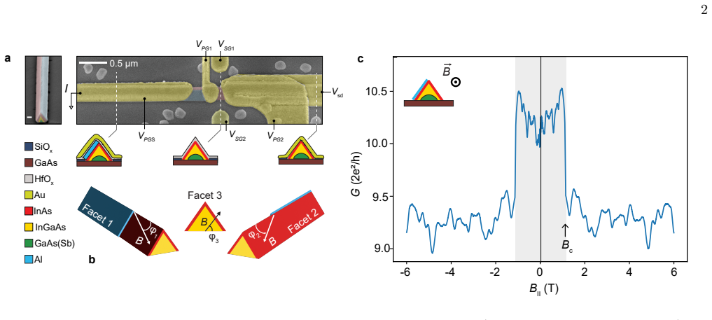


read the original abstract
Understanding the spatial distribution of carriers is important for interpreting transport in nanoscale devices. Here, we apply conductance fluctuation tomography to planar selective-area-grown InAs nanowires in both normal-normal and normal-superconductor device geometries. By tracking the evolution of conductance-interference features as a function of magnetic-field strength and orientation, we extract information about the geometry of phase-coherent transport pathways. Using theory to distinguish between bulk-dominated transport, coherent near-surface transport across facets, and transport confined to individual facets. The measurements are consistent with transport dominated by a near-surface accumulation layer in InAs. Devices with normal contacts show behavior consistent with coherent transport across the nanowire apex, whereas hybrid normal-superconductor devices exhibit signatures of more facet-dependent transport. These results demonstrate how universal conductance fluctuations can be used as a tomographic probe of phase-coherent transport pathways in semiconductor nanostructures.
Editorial analysis
A structured set of objections, weighed in public.
Referee Report
Summary. The manuscript applies conductance fluctuation tomography to selective-area-grown InAs nanowires in normal-normal and normal-superconductor geometries. By tracking the evolution of interference features versus magnetic-field strength and orientation, the authors use theory to distinguish bulk-dominated, coherent near-surface (across facets), and facet-confined transport, concluding that a near-surface accumulation layer dominates. NN devices are interpreted as showing apex-coherent transport while NS devices show more facet-dependent behavior.
Significance. If the theoretical mapping from fluctuation patterns to geometry is robust, the work offers a tomographic probe of phase-coherent pathways that could be useful for characterizing carrier distributions in semiconductor nanowires without invasive imaging. The dual NN/NS comparison provides an internal consistency check on the interpretation.
major comments (1)
- [Theory and comparison sections] The central claim that the data support near-surface accumulation-layer transport (rather than bulk or single-facet confinement) rests on the theoretical modeling of interference evolution with B-field strength and orientation. The manuscript must demonstrate that this mapping is unique by showing explicit theory curves, parameter sensitivity, or goodness-of-fit metrics that rule out alternative geometries for the selective-area-grown cross-section; without such evidence the distinction remains under-determined.
minor comments (2)
- Clarify the precise definition of 'angle-resolved' conductance fluctuations and how the magnetic-field orientation is controlled experimentally.
- Include error bars or statistical measures on the extracted interference features to allow assessment of the robustness of the regime distinctions.
Simulated Author's Rebuttal
We thank the referee for their detailed review and constructive criticism. The point raised about demonstrating the uniqueness of the theoretical mapping is well taken, and we will strengthen the manuscript accordingly.
read point-by-point responses
-
Referee: [Theory and comparison sections] The central claim that the data support near-surface accumulation-layer transport (rather than bulk or single-facet confinement) rests on the theoretical modeling of interference evolution with B-field strength and orientation. The manuscript must demonstrate that this mapping is unique by showing explicit theory curves, parameter sensitivity, or goodness-of-fit metrics that rule out alternative geometries for the selective-area-grown cross-section; without such evidence the distinction remains under-determined.
Authors: We agree that the current presentation of the theoretical modeling would benefit from more explicit comparisons to establish uniqueness. The manuscript already contains calculations distinguishing bulk, near-surface, and single-facet regimes, but we acknowledge that additional figures showing full theory curves for each geometry, parameter sensitivity analysis, and quantitative goodness-of-fit metrics are needed to rigorously rule out alternatives. In the revised version we will add these elements to the theory and comparison sections, including supplementary material with the requested plots and metrics for the selective-area-grown cross-section. revision: yes
Circularity Check
No circularity; experimental claims rest on data-theory comparison without self-referential reduction.
full rationale
The paper is an experimental study of conductance fluctuations in selective-area-grown InAs nanowires. It reports measurements in NN and NS device geometries and states that theory is used to interpret the evolution of interference features with magnetic field strength and orientation, leading to the conclusion of near-surface accumulation layer transport. No equations, fitted parameters renamed as predictions, or self-citations are present in the abstract or described text that would make the central claims equivalent to their inputs by construction. The distinction between bulk, near-surface, and facet-confined transport is presented as arising from external theoretical modeling applied to the data, rendering the derivation self-contained.
Axiom & Free-Parameter Ledger
Reference graph
Works this paper leans on
-
[1]
Krizek, J
F. Krizek, J. E. Sestoft, P. Aseev, S. Marti-Sanchez, S. Vaitiek˙ enas, L. Casparis, S. A. Khan, Y. Liu, T. c. v. Stankeviˇ c, A. M. Whiticar, A. Fursina, F. Boekhout, R. Koops, E. Uccelli, L. P. Kouwenhoven, C. M. Mar- cus, J. Arbiol, and P. Krogstrup, Phys. Rev. Mater.2, 093401 (2018)
2018
-
[3]
Olˇ steins, G
D. Olˇ steins, G. Nagda, D. J. Carrad, D. V. Beznasyuk, C. E. Petersen, S. Mart´ ı-S´ anchez, J. Arbiol, and T. S. Jespersen, Nature communications14, 7738 (2023)
2023
-
[4]
Olsteins, G
D. Olsteins, G. Nagda, D. J. Carrad, D. V. Beznasyuk, C. E. N. Petersen, S. Mart´ ı-S´ anchez, J. Arbiol, and T. S. Jespersen, Nano Letters24, 6553–6559 (2024)
2024
-
[5]
Alicea, Y
J. Alicea, Y. Oreg, G. Refael, F. Von Oppen, and M. P. Fisher, Nature Physics7, 412 (2011)
2011
-
[6]
Nadj-Perge, S
S. Nadj-Perge, S. M. Frolov, E. P. A. M. Bakkers, and L. P. Kouwenhoven, Nature468, 1084–1087 (2010)
2010
-
[7]
W. Peng, Z. Aksamija, S. A. Scott, J. J. Endres, D. E. Savage, I. Knezevic, M. A. Eriksson, and M. G. Lagally, Nature Communications4, 1339 (2013)
2013
-
[8]
J. W. W. van Tilburg, R. E. Algra, G. Immink, M. A. Verheijen, E. P. A. M. Bakkers, and L. P. Kouwenhoven, Semiconductor Science and Technology 25, 024011 (2010)
2010
-
[9]
Wang and M
J. Wang and M. S. Gudiksen, Nanotechnology24, 375202 (2013)
2013
-
[10]
L. O. Olsson, C. B. M. Andersson, M. C. H˚ akansson, J. Kanski, L. Ilver, and U. O. Karlsson, Phys. Rev. Lett. 76, 3626 (1996)
1996
-
[11]
Dayeh, D
S. Dayeh, D. P. Aplin, X. Zhou, P. K. Yu, E. Yu, and D. Wang, Small3, 326 (2007)
2007
-
[12]
A. C. Ford, J. C. Ho, Y.-L. Chueh, Y.-C. Tseng, Z. Fan, J. Guo, J. Bokor, and A. Javey, Nano Letters9, 360 (2009)
2009
-
[13]
V. E. Degtyarev, S. V. Khazanova, and N. V. Demarina, Scientific Reports7, 3411 (2017)
2017
-
[14]
Gupta, IEEE Transactions on Electron Devices41, 2093 (1994)
M. Gupta, IEEE Transactions on Electron Devices41, 2093 (1994)
2093
-
[15]
P. A. Lee and A. D. Stone, Physical Review Letters55, 1622 (1985), publisher: American Physical Society
1985
-
[16]
Imry, Europhysics Letters1, 249 (1986)
Y. Imry, Europhysics Letters1, 249 (1986)
1986
-
[17]
P. A. Mello, Physical Review Letters60, 1089 (1988), publisher: American Physical Society
1988
-
[18]
P. A. Lee, A. D. Stone, and H. Fukuyama, Physical Re- view B35, 1039 (1987), publisher: American Physical Society
1987
-
[19]
C. W. J. Beenakker, Reviews of Modern Physics69, 731 (1997), publisher: American Physical Society
1997
-
[20]
Scheer, H
E. Scheer, H. von L¨ ohneysen, A. D. Mirlin, P. W¨ olfle, and H. Hein, Physical Review Letters78, 3362 (1997)
1997
-
[21]
Liang, J
D. Liang, J. Du, and X. P. A. Gao, Phys. Rev. B81, 153304 (2010)
2010
-
[22]
F. Haas, T. Wenz, P. Zellekens, N. Demarina, T. Rieger, M. Lepsa, D. Gr¨ utzmacher, H. L¨ uth, and T. Sch¨ apers, Scientific Reports6, 24573 (2016)
2016
-
[23]
T. S. Jespersen, J. R. Hauptmann, C. B. Sørensen, and J. Nyg˚ ard, Phys. Rev. B91, 041302 (2015)
2015
-
[24]
D. V. Beznasyuk, S. Mart´ ı-S´ anchez, J.-H. Kang, R. Tanta, M. Rajpalke, T. c. v. Stankeviˇ c, A. W. Chris- tensen, M. C. Spadaro, R. Bergamaschini, N. N. Maka, C. E. N. Petersen, D. J. Carrad, T. S. Jespersen, J. Ar- biol, and P. Krogstrup, Phys. Rev. Mater.6, 034602 (2022)
2022
-
[25]
Trevisan, P
A. Trevisan, P. D. Hodgson, F. Alvarado-C´ esar, M. Hayne, R. Beanland, and P. M. Koenraad, Journal of Applied Physics137, 195702 (2025)
2025
-
[26]
M. E. n. Cachaza, A. W. Christensen, D. Beznasyuk, T. Særkjær, M. H. Madsen, R. Tanta, G. Nagda, S. Schuwalow, and P. Krogstrup, Phys. Rev. Mater.5, 094601 (2021)
2021
-
[27]
C. W. J. Beenakker, Physical Review B47, 15763 (1993), publisher: American Physical Society. Supplemental Material for: Tomography of Transport Pathways in Selective-Area-Grown Nanowires Using Angle-Resolved Conductance Fluctuations Christian E. N. Petersen, 1,∗ Damon J. Carrad, 1 Daria Beznasyuk, 1 and Thomas S. Jespersen 1 1Department of Energy Conversi...
1993
discussion (0)
Sign in with ORCID, Apple, or X to comment. Anyone can read and Pith papers without signing in.