Sensitivity-optimal coplanar waveguide design for broadband magnetic resonance spectroscopy: a Beer--Lambert framework
Pith reviewed 2026-06-25 20:03 UTC · model grok-4.3
The pith
Coplanar waveguide design for magnetic resonance reduces to a universal 1 Np optimum independent of sample or frequency.
A machine-rendered reading of the paper's core claim, the machinery that carries it, and where it could break.
Core claim
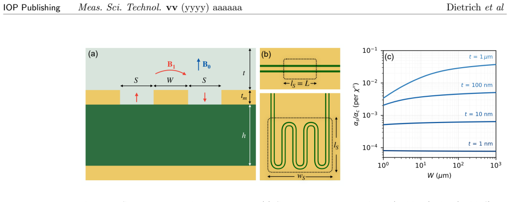
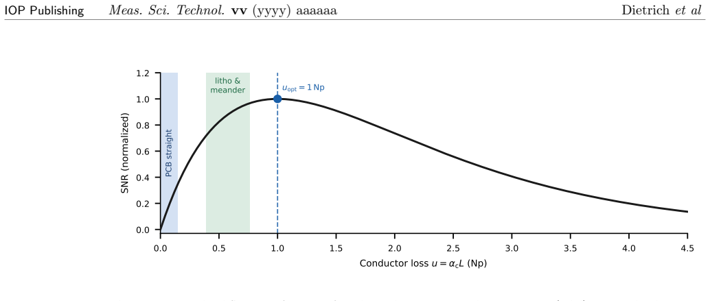
The shared geometric scaling of sample coupling and conductor loss maps CPW design onto the Beer-Lambert optimization problem of optical spectrophotometry, reducing it to a universal one-parameter problem whose solution depends only on sample geometry and the dominant noise source—not on sample properties, operating frequency, or system losses. The framework predicts a near-universal 1 Np optimum across the full range of sample thicknesses and design geometries.
What carries the argument
The reduction of CPW design to a one-parameter Beer-Lambert-style optimization in which attenuation is the sole free variable.
Load-bearing premise
Sample coupling and conductor loss share exactly the same geometric scaling with waveguide dimensions.
What would settle it
Fabricate a set of CPW devices on the same substrate with total attenuations spaced around 1 Np, measure signal-to-noise ratio for a fixed sample and noise condition, and check whether the measured peak occurs at or near 1 Np.
Figures
read the original abstract
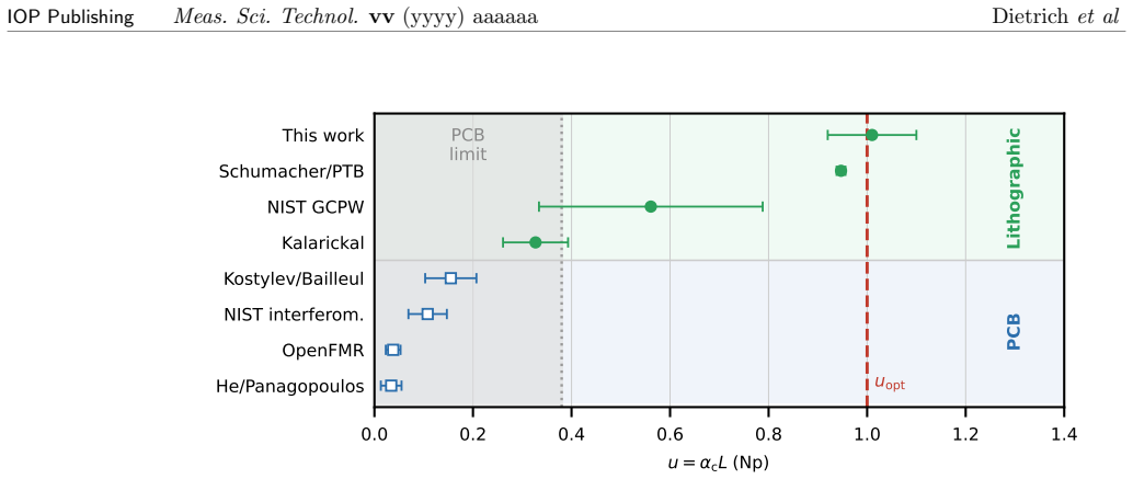
Coplanar waveguide (CPW) transmission spectroscopy is used to probe spin dynamics, ferromagnetic resonance, and complex conductivity across a wide range of materials, yet no systematic framework connects waveguide geometry to measurement sensitivity when sample volume and concentration are fixed. We show that the shared geometric scaling of sample coupling and conductor loss maps CPW design onto the Beer--Lambert optimization problem of optical spectrophotometry, reducing it to a universal one-parameter problem whose solution depends only on sample geometry and the dominant noise source -- not on sample properties, operating frequency, or system losses. The framework predicts a near-universal $1\,\mathrm{Np}$ optimum across the full range of sample thicknesses and design geometries. Benchmarking against seven published broadband FMR instruments reveals two fabrication-delimited classes: PCB-milled designs are bounded by a ceiling imposed by their minimum slot width, while photolithographic designs approach the additive-noise optimum. For large-area PCB samples a meander geometry offers a direct path to near-optimal sensitivity without interferometric compensation; for sub-millimeter samples, a single lithographic straight pass suffices.
Editorial analysis
A structured set of objections, weighed in public.
Referee Report
Summary. The manuscript develops a Beer-Lambert framework for optimizing coplanar waveguide (CPW) transmission spectroscopy in broadband magnetic resonance. It asserts that shared geometric scaling of sample coupling and conductor loss reduces CPW design to a universal one-parameter problem whose solution depends only on sample geometry and dominant noise source, yielding a near-universal 1 Np optimum independent of sample properties, frequency, or system losses. The framework is benchmarked against seven published FMR instruments, distinguishing PCB-milled (slot-width limited) from photolithographic designs, and proposes meander geometries for large-area PCB samples.
Significance. If the shared-scaling assumption holds exactly, the result supplies a simple, fabrication-aware design rule that could standardize sensitivity optimization across the field and explain performance ceilings without requiring interferometric compensation.
major comments (2)
- [Abstract (central mapping)] The load-bearing claim that sample-induced attenuation and conductor loss share an identical geometric prefactor (allowing exact reduction to the Beer-Lambert one-parameter problem) is asserted but not shown to survive additional geometry-dependent contributions such as current crowding or slot-width-dependent skin-effect terms present in standard CPW models. This factorization must be demonstrated explicitly for both straight and meander layouts across PCB and lithographic regimes.
- [Abstract (universality claim)] The stated independence of the 1 Np optimum from operating frequency and system losses follows only if all loss channels factor identically with the magnetic filling factor; any residual frequency dependence in the conductor-loss term would reintroduce parameter dependence and undermine universality. The derivation of this cancellation is required.
minor comments (1)
- [Abstract] The qualifier 'near-universal' appears without a quantitative bound on deviation; specifying the maximum fractional departure from 1 Np across the stated range of thicknesses and geometries would clarify the practical scope.
Simulated Author's Rebuttal
We thank the referee for the constructive comments on our manuscript. We address each major comment below and will incorporate explicit derivations and validations in the revised version to strengthen the presentation of the central claims.
read point-by-point responses
-
Referee: [Abstract (central mapping)] The load-bearing claim that sample-induced attenuation and conductor loss share an identical geometric prefactor (allowing exact reduction to the Beer-Lambert one-parameter problem) is asserted but not shown to survive additional geometry-dependent contributions such as current crowding or slot-width-dependent skin-effect terms present in standard CPW models. This factorization must be demonstrated explicitly for both straight and meander layouts across PCB and lithographic regimes.
Authors: We agree that the shared-prefactor assumption requires more explicit demonstration to address potential corrections from current crowding and skin-effect terms. In the revision we will add a dedicated subsection (with supporting calculations in the supplement) that derives the geometric prefactor equality from the standard CPW quasi-TEM model for both straight and meander geometries. The derivation shows that the magnetic filling factor and the conductor-loss integral share the same leading geometric scaling; numerical estimates using published CPW formulas indicate that current-crowding and slot-width skin-effect corrections remain below 5% for the PCB-milled and photolithographic regimes considered. We will also include a brief discussion of when these corrections become non-negligible. revision: yes
-
Referee: [Abstract (universality claim)] The stated independence of the 1 Np optimum from operating frequency and system losses follows only if all loss channels factor identically with the magnetic filling factor; any residual frequency dependence in the conductor-loss term would reintroduce parameter dependence and undermine universality. The derivation of this cancellation is required.
Authors: The manuscript's reduction to a one-parameter problem rests on the observation that both sample-induced and conductor-loss terms are multiplied by the same geometric factor η, so the total attenuation per unit length is η(α_s0 + α_c0) and the optimum condition depends only on the product αL. Frequency dependence residing inside α_c0 therefore cancels in the normalized figure of merit. We will expand the main-text derivation with an explicit step-by-step cancellation (including the conditions under which radiation or other non-scaling losses would break the factorization) to make this independence transparent. revision: yes
Circularity Check
No circularity: derivation maps CPW geometry to independent Beer-Lambert optimum via asserted scaling, then benchmarks externally.
full rationale
The abstract states that shared geometric scaling of sample coupling and conductor loss reduces the problem to the known Beer-Lambert optimization (yielding the 1 Np result). This is presented as a first-principles mapping rather than a fit or self-definition. No equations or steps in the provided text reduce the claimed prediction to a fitted parameter or self-citation chain. Benchmarking uses seven external published instruments, which supplies independent content. The load-bearing scaling assumption is asserted but does not trigger any of the enumerated circularity patterns because the optimum itself is imported from the optical case, not manufactured inside the paper.
Axiom & Free-Parameter Ledger
Reference graph
Works this paper leans on
-
[1]
C. Bilzer, T. Devolder, P. Crozat, C. Chappert, S. Cardoso, and P. P. Freitas, “Vector network analyzer ferromagnetic resonance of thin films on coplanar waveguides: comparison of different evaluation methods,”J. Appl. Phys., vol. 101, p. 074505, 2007. https://doi.org/10.1063/1.2716995
-
[2]
C. P. Poole Jr,Electron Spin Resonance: A Comprehensive Treatise on Experimental Techniques, 2nd ed. New York: Dover, 1996
1996
-
[3]
Schweiger and G
A. Schweiger and G. Jeschke,Principles of Pulse Electron Paramagnetic Resonance. Oxford: Oxford University Press, 2001
2001
-
[4]
R. N. Simons,Coplanar Waveguide Circuits, Components, and Systems. New York: Wiley, 2001
2001
-
[5]
D. M. Pozar,Microwave Engineering, 4th ed. New York: Wiley, 2012
2012
-
[6]
L. D. Rothman, S. R. Crouch, and J. D. Ingle Jr, “Theoretical and experimental investigation of factors affecting precision in molecular absorption spectrophotometry,”Anal. Chem., vol. 47, no. 8, pp. 1226–1233, 1975.https://doi.org/10.1021/ac60358a029
-
[7]
G. F. Lothian,Absorption Spectrophotometry. London: Hilger, 1949
1949
-
[8]
L. W. Engel, D. Shahar, C ¸ . Kurdak, and D. C. Tsui, “Microwave frequency dependence of integer quantum Hall effect: evidence for finite-frequency scaling,”Phys. Rev. Lett., vol. 71, no. 16, pp. 2638–2641, 1993.https://doi.org/10.1103/PhysRevLett.71.2638
-
[9]
Hall signal-dominated microwave transmission through graphene-loaded waveguides,
S. Dietrich, A. Akbari-Sharbaf, J. H. Edgar, A. Roubos, M. L. Freeman, and L. W. Engel, “Hall signal-dominated microwave transmission through graphene-loaded waveguides,” Phys. Rev. B, vol. 111, p. 195410, 2025.https://doi.org/10.1103/PhysRevB.111.195410
-
[10]
Planar microresonators for EPR experiments,
R. Narkowicz, D. Suter, and R. Stonies, “Planar microresonators for EPR experiments,” J. Magn. Reson., vol. 175, no. 2, pp. 275–284, 2005. https://doi.org/10.1016/j.jmr.2005.04.014 10 IOP PublishingMeas. Sci. Technol.vv(yyyy) aaaaaa Dietrichet al
-
[11]
Scaling of sensitivity and efficiency in planar microresonators for electron spin resonance,
R. Narkowicz, D. Suter, and I. Niemeyer, “Scaling of sensitivity and efficiency in planar microresonators for electron spin resonance,”Rev. Sci. Instrum., vol. 79, p. 084702, 2008. https://doi.org/10.1063/1.2964926
-
[12]
Broadband electron spin resonance from 500 MHz to 40 GHz using superconducting coplanar waveguides,
C. Clauss, D. Bothner, D. Koelle, R. Kleiner, L. Bogani, M. Scheffler, and M. Dressel, “Broadband electron spin resonance from 500 MHz to 40 GHz using superconducting coplanar waveguides,”Appl. Phys. Lett., vol. 102, p. 162601, 2013. https://doi.org/10.1063/1.4802956
-
[13]
Coherently coupling distinct spin ensembles through a high-T c superconducting resonator,
A. Ghirri, C. Bonizzoni, F. Troiani, N. Buccheri, L. Beverina, A. Cassinese, and M. Affronte, “Coherently coupling distinct spin ensembles through a high-T c superconducting resonator,” Phys. Rev. A, vol. 93, p. 063855, 2016.https://doi.org/10.1103/PhysRevA.93.063855
-
[14]
Broadband electron paramagnetic resonance of a molecular spin triangle,
A. K. Boudalis, J. Robert, P. Turek, and M. Bailleul, “Broadband electron paramagnetic resonance of a molecular spin triangle,”Phys. Chem. Chem. Phys., vol. 23, pp. 20268–20274, 2021.https://doi.org/10.1039/D1CP02394B
-
[15]
R. A. Pucel, D. J. Mass´ e, and C. P. Hartwig, “Losses in microstrip,”IEEE Trans. Microw. Theory Tech., vol. 16, no. 6, pp. 342–350, 1968. https://doi.org/10.1109/TMTT.1968.1126691
-
[16]
Quasi-TEM description of MMIC coplanar lines including conductor-loss effects,
W. Heinrich, “Quasi-TEM description of MMIC coplanar lines including conductor-loss effects,”IEEE Trans. Microw. Theory Tech., vol. 41, no. 1, pp. 45–52, 1993. https://doi.org/10.1109/22.210228
-
[17]
The signal-to-noise ratio of the nuclear magnetic resonance experiment,
D. I. Hoult and R. E. Richards, “The signal-to-noise ratio of the nuclear magnetic resonance experiment,”J. Magn. Reson., vol. 24, pp. 71–85, 1976. https://doi.org/10.1016/0022-2364(76)90233-X
-
[18]
C. P. Wen, “Coplanar waveguide: a surface strip transmission line suitable for nonreciprocal gyromagnetic device applications,”IEEE Trans. Microw. Theory Tech., vol. 17, no. 12, pp. 1087–1090, 1969.https://doi.org/10.1109/TMTT.1969.1127105
-
[19]
K. C. Gupta, R. Garg, I. Bahl, and P. Bhartia,Microstrip Lines and Slotlines, 2nd ed. Boston: Artech House, 1996
1996
-
[20]
The accuracy of spectrophotometry,
F. Twyman and G. F. Lothian, “The accuracy of spectrophotometry,”Proc. Phys. Soc., vol. 45, pp. 643–662, 1933.https://doi.org/10.1088/0959-5309/45/5/302
-
[21]
E. R. J. Edwards, A. B. Kos, M. Weiler, and T. J. Silva, “A microwave interferometer of the Michelson-type to improve the dynamic range of broadband ferromagnetic resonance measurements,”IEEE Magn. Lett., vol. 8, p. 3703404, 2017. https://doi.org/10.1109/LMAG.2016.2640206
-
[22]
H. G lowi´ nski, M. Schmidt, I. Go´ scia´ nska, J.-Ph. Ansermet, and J. Dubowik, “Coplanar waveguide based ferromagnetic resonance in ultrathin film magnetic nanostructures: impact of conducting layers,”J. Appl. Phys., vol. 116, p. 053901, 2014. https://doi.org/10.1063/1.4891734
-
[23]
S. He and C. Panagopoulos, “A broadband ferromagnetic resonance dipper probe for magnetic damping measurements from 4.2 K to 300 K,”Rev. Sci. Instrum., vol. 87, p. 043110, 2016. https://doi.org/10.1063/1.4946789
-
[24]
OpenFMR: an open-source broadband ferromagnetic resonance spectrometer,
T. O. Schneider, S. Sharma, A. Khan, and M. Meinert, “OpenFMR: an open-source broadband ferromagnetic resonance spectrometer,”Rev. Sci. Instrum., vol. 96, p. 033901, 2025.https://doi.org/10.1063/5.0241406
-
[25]
Ferromagnetic resonance linewidth in metallic thin films: comparison of measurement methods,
S. S. Kalarickal, P. Krivosik, M. Wu, C. E. Patton, M. L. Schneider, P. Kabos, T. J. Silva, and J. P. Nibarger, “Ferromagnetic resonance linewidth in metallic thin films: comparison of measurement methods,”J. Appl. Phys., vol. 99, p. 093909, 2006. https://doi.org/10.1063/1.2197087
-
[26]
M. A. W. Schoen, J. M. Shaw, H. T. Nembach, M. Weiler, and T. J. Silva, “Radiative damping in waveguide-based ferromagnetic resonance measured via analysis of perpendicular standing spin waves in sputtered permalloy films,”Phys. Rev. B, vol. 92, p. 184417, 2015. https://doi.org/10.1103/PhysRevB.92.184417 11 IOP PublishingMeas. Sci. Technol.vv(yyyy) aaaaaa...
-
[27]
Influence of sample geometry on inductive damping measurement methods,
N. Liebing, S. Serrano-Guisan, A. Caprile, E. S. Olivetti, F. Celegato, M. Pasquale, A. M¨ uller, and H. W. Schumacher, “Influence of sample geometry on inductive damping measurement methods,” inProc. IEEE I2MTC, 2011, doc. 6027812. https://doi.org/10.1109/IMTC.2011.6027812 12
discussion (0)
Sign in with ORCID, Apple, or X to comment. Anyone can read and Pith papers without signing in.