Hidden Defect Chemistry in Ion-Irradiated MoS₂ Field-Effect Transistors Revealed by Photocurrent Loss
Pith reviewed 2026-06-30 04:58 UTC · model grok-4.3
The pith
Photocurrent loss under 532 nm light reveals irradiation-induced sulfur vacancy changes in MoS2 transistors that remain hidden in dark measurements due to hydrocarbon passivation from carbon residues.
A machine-rendered reading of the paper's core claim, the machinery that carries it, and where it could break.
Core claim
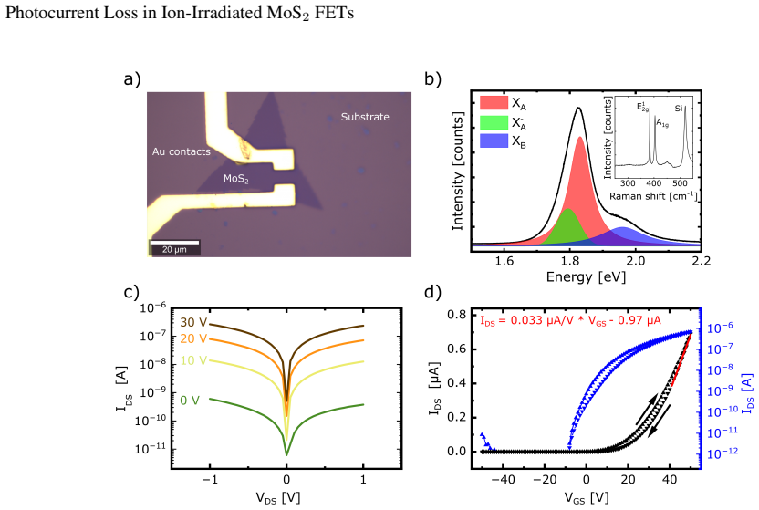
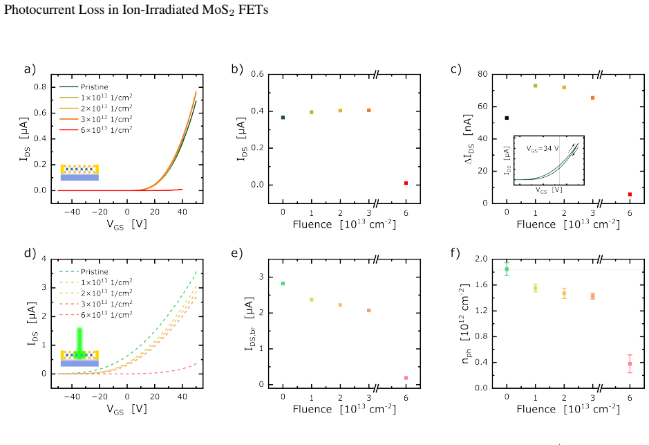
Low-energy 40 eV Ar+ irradiation preferentially generates sulfur vacancies in the MoS2 channel while limiting substrate damage. Dark transfer characteristics remain robust up to moderate fluences and degrade only at the highest fluence. Under 532 nm illumination, photocurrent and photodoping decrease systematically with increasing fluence, exposing the irradiation-induced changes. Atomic force microscopy and X-ray photoelectron spectroscopy detect substantial carbon-containing residues even after extended cleaning. These residues are proposed to act as a reservoir for hydrocarbon-mediated passivation of the vacancies. Density-functional-theory calculations show that unsaturated vacancies int
What carries the argument
Hydrocarbon-mediated passivation of sulfur vacancies by persistent carbon-containing surface residues, which suppresses in-gap states according to the DFT model of H-Cs configurations.
If this is right
- Dark transfer curves show apparent robustness against irradiation up to moderate fluences, with degradation appearing only at the highest fluence.
- Photocurrent and light-induced photodoping decrease systematically with ion fluence under 532 nm illumination.
- Atomic force microscopy and X-ray photoelectron spectroscopy confirm persistent carbon residues that can serve as a passivation reservoir.
- Density-functional-theory calculations establish that unsaturated sulfur vacancies create in-gap states while H-Cs configurations remove them.
Where Pith is reading between the lines
- Photocurrent measurements under above-band-gap light may function as a general probe for detecting passivated defects across other processed two-dimensional material devices.
- Processing-induced carbon contamination should be treated as a systematic variable in any defect-engineering study of transition-metal dichalcogenides rather than an incidental factor.
- Alternative surface-cleaning protocols or in-situ characterization under illumination could unmask vacancy effects that current dark-only workflows miss.
Load-bearing premise
Carbon-containing residues that remain on processed devices supply a reservoir enabling hydrocarbon-mediated passivation of the irradiation-created sulfur vacancies.
What would settle it
Thorough removal of all carbon residues before irradiation followed by the same fluence series would produce immediate degradation in dark transfer curves and eliminate the systematic photocurrent drop with fluence.
Figures


read the original abstract
Defect engineering in monolayer MoS$_2$ is a promising route to tune field-effect transistors (FETs), but the electronic response of defects in processed devices can be masked by contacts, substrate effects, adsorbates, and chemical passivation. Here, we irradiate MoS$_2$ FETs with low-energy 40~eV Ar$^+$ ions to preferentially create sulfur vacancies (V$_S$) in the channel while minimizing substrate damage. We compare dark and illuminated electrical characterization with surface analysis and first-principles calculations. Dark transfer characteristics show an apparent robustness against irradiation up to moderate fluences, with pronounced degradation only at the highest fluence. Under 532~nm illumination, however, the photocurrent and light-induced photodoping decrease systematically with increasing ion fluence, revealing irradiation-induced changes that are hidden in standard dark measurements. Atomic force microscopy and X-ray photoelectron spectroscopy show substantial carbon-containing residues on processed devices even after extended cleaning. We propose that such residues may provide a reservoir for hydrocarbon-mediated passivation of sulfur vacancies. Density-functional-theory calculations provide a microscopic model consistent with this scenario: unsaturated V$_S$ introduce in-gap states, H-C$_S$ configurations suppress these states, and carbon substitution without hydrogen leaves defect states in the band gap. Our results highlight carbon-containing surface contamination as a key factor in interpreting defect engineering experiments on MoS$_2$ and related TMDC devices.
Editorial analysis
A structured set of objections, weighed in public.
Referee Report
Summary. The manuscript claims that low-energy (40 eV) Ar+ irradiation of monolayer MoS2 FETs preferentially creates sulfur vacancies (VS) whose electronic effects are masked in dark transport by hydrocarbon passivation from carbon-containing surface residues. Dark transfer curves remain robust up to moderate fluences, but 532 nm photocurrent and light-induced photodoping decrease systematically with fluence. AFM/XPS detect persistent carbon residues after cleaning; DFT shows that H-CS configurations suppress the in-gap states of bare VS while CS does not. The work concludes that carbon contamination must be considered when interpreting defect-engineering results in TMDC devices.
Significance. If the passivation mechanism is confirmed, the result would be significant for defect engineering in 2D materials because it shows how standard dark measurements can miss irradiation-induced changes and demonstrates the diagnostic value of photocurrent. The fluence-dependent optical response, surface spectroscopy, and DFT together constitute a coherent multi-probe strategy; the explicit identification of H-CS as a passivating species is a concrete microscopic hypothesis that can be tested further.
major comments (3)
- [Surface analysis and discussion of passivation mechanism] The central claim that hydrocarbon passivation of VS explains the hidden photocurrent loss rests on correlative AFM/XPS detection of carbon residues plus DFT, but lacks fluence-dependent quantification of passivated versus unsaturated VS densities or direct controls that remove carbon (different substrates, UHV processing). This chain is load-bearing for the interpretation.
- [Illuminated electrical characterization] Alternative fluence-dependent mechanisms that could reduce photocurrent only under illumination (e.g., substrate adsorbates, contact barrier changes, or mobility degradation) are not quantitatively compared to the passivation model or ruled out by additional controls.
- [DFT calculations] DFT results establish that H-CS removes in-gap states while bare VS and CS do not, yet the calculations are not used to predict the expected magnitude or spectral dependence of the photocurrent drop, leaving the link to the experimental fluence trend qualitative.
minor comments (2)
- [Figures and experimental results] Error bars and number of devices measured should be stated explicitly for all fluence-dependent photocurrent and threshold-voltage data.
- [Methods] The ion fluence values and exact cleaning protocols could be tabulated for reproducibility.
Simulated Author's Rebuttal
We thank the referee for the constructive comments and the positive assessment of the work's significance. We address each major comment below with clarifications and proposed revisions.
read point-by-point responses
-
Referee: The central claim that hydrocarbon passivation of VS explains the hidden photocurrent loss rests on correlative AFM/XPS detection of carbon residues plus DFT, but lacks fluence-dependent quantification of passivated versus unsaturated VS densities or direct controls that remove carbon (different substrates, UHV processing). This chain is load-bearing for the interpretation.
Authors: We agree that fluence-dependent quantification of passivated versus unsaturated VS and direct controls (e.g., UHV processing or alternative substrates) would provide stronger evidence. In the revised manuscript, we will add quantitative analysis of existing XPS C 1s spectra to estimate carbon coverage trends with fluence and include an expanded discussion section explicitly addressing the correlative nature of the evidence, the limitations of current controls, and recommendations for future experiments. The systematic photocurrent fluence dependence (absent in dark data) together with AFM/XPS and the DFT model remains consistent with the proposed mechanism. revision: partial
-
Referee: Alternative fluence-dependent mechanisms that could reduce photocurrent only under illumination (e.g., substrate adsorbates, contact barrier changes, or mobility degradation) are not quantitatively compared to the passivation model or ruled out by additional controls.
Authors: We will revise the manuscript to add a dedicated comparison of alternatives. Mobility degradation is inconsistent with the observed robustness of dark transfer curves up to moderate fluences. Contact barrier modifications would be expected to appear in dark characteristics as well. Substrate adsorbates are mitigated by the described cleaning protocols and are directly addressed by the persistent carbon detected in post-cleaning XPS and AFM. These points will be quantified and discussed relative to the passivation model using the existing dataset. revision: yes
-
Referee: DFT results establish that H-CS removes in-gap states while bare VS and CS do not, yet the calculations are not used to predict the expected magnitude or spectral dependence of the photocurrent drop, leaving the link to the experimental fluence trend qualitative.
Authors: The DFT calculations supply a microscopic model explaining why illumination reveals the defects while dark transport does not. We acknowledge that the connection to the experimental fluence trend is qualitative. In the revision we will add explicit text stating that quantitative prediction of photocurrent magnitude or spectral dependence would require device-scale transport simulations that incorporate the calculated defect levels, which lies beyond the present scope. The 532 nm data are noted as consistent with involvement of the in-gap states identified by DFT. revision: partial
Circularity Check
No circularity: experimental photocurrent trends, surface spectroscopy, and independent DFT are self-contained.
full rationale
The paper's central claim rests on direct experimental observations (fluence-dependent photocurrent loss under 532 nm illumination versus robustness in dark) combined with AFM/XPS detection of carbon residues and separate first-principles DFT modeling of defect states (unsaturated V_S vs. H-C_S). No equations reduce by construction to fitted inputs, no predictions are statistically forced from the target data, and no load-bearing steps invoke self-citations or imported uniqueness theorems. The interpretation of hydrocarbon passivation is presented as a proposal consistent with the data rather than a derivation that collapses to its own inputs.
Axiom & Free-Parameter Ledger
axioms (1)
- domain assumption Density-functional-theory calculations with standard approximations accurately capture the in-gap states of V_S and their modification by H-C_S configurations in monolayer MoS2.
invented entities (1)
-
H-C_S configurations
no independent evidence
Reference graph
Works this paper leans on
-
[1]
Time-evolution of the electrical characteris- tics of MoS2 field-effect transistors after electron beam irradiation.Phys
Ming-Yen Lu, Shang-Chi Wu, Hsiang-Chen Wang, and Ming-Pei Lu. Time-evolution of the electrical characteris- tics of MoS2 field-effect transistors after electron beam irradiation.Phys. Chem. Chem. Phys., 20(14):9038–9044, 2018
2018
-
[2]
Electron irradiation of metal contacts in monolayer MoS2 field-effect transistors.ACS Appl
Aniello Pelella, Osamah Kharsah, Alessandro Grillo, Francesca Urban, Maurizio Passacantando, Filippo Giubileo, Laura Iemmo, Stephan Sleziona, Erik Pollmann, Lukas Madauß, Marika Schleberger, and Antonio Di Bartolomeo. Electron irradiation of metal contacts in monolayer MoS2 field-effect transistors.ACS Appl. Mater . Interfaces, 12(36):40532–40540, 2020
2020
-
[3]
Manipulation of the electrical and memory properties of MoS 2 field-effect transistors by highly charged ion irradiation.Nanoscale Adv., 5(24):6958–6966, 2023
Stephan Sleziona, Aniello Pelella, Enver Faella, Osamah Kharsah, Lucia Skopinski, André Maas, Yossarian Liebsch, Jennifer Schmeink, Antonio Di Bartolomeo, and Marika Schleberger. Manipulation of the electrical and memory properties of MoS 2 field-effect transistors by highly charged ion irradiation.Nanoscale Adv., 5(24):6958–6966, 2023
2023
-
[4]
Engineering chemically active defects in monolayer MoS 2 transistors via ion-beam irradiation and their healing via vapor deposition of alkanethiols.Adv
Simone Bertolazzi, Sara Bonacchi, Guangjun Nan, Anton Pershin, David Beljonne, and Paolo Samorì. Engineering chemically active defects in monolayer MoS 2 transistors via ion-beam irradiation and their healing via vapor deposition of alkanethiols.Adv. Mater ., 29(18):1606760, 2017
2017
-
[5]
Cullen, Yangbo Zhou, Huading Song, Clive Downing, Daniel Fox, Niall McEvoy, Rui Zhu, Jun Xu, Georg S
Jakub Jadwiszczak, Darragh Keane, Pierce Maguire, Conor P. Cullen, Yangbo Zhou, Huading Song, Clive Downing, Daniel Fox, Niall McEvoy, Rui Zhu, Jun Xu, Georg S. Duesberg, Zhi-Min Liao, John J. Boland, and Hongzhou Zhang. MoS 2 memtransistors fabricated by localized helium ion beam irradiation.ACS Nano, 13(12):14262–14273, 2019
2019
-
[6]
Low-defect-density monolayer MoS2 wafer by oxygen-assisted growth-repair strategy.Adv
Xiaomin Zhang, Jiahan Xu, Aomiao Zhi, Jian Wang, Yue Wang, Wenkai Zhu, Xingjie Han, Xuezeng Tian, Xuedong Bai, Baoquan Sun, Zhongming Wei, Jing Zhang, and Kaiyou Wang. Low-defect-density monolayer MoS2 wafer by oxygen-assisted growth-repair strategy.Adv. Sci., 11(42):e2408640, 2024
2024
-
[7]
Antonio Di Bartolomeo, Luca Genovese, Tobias Foller, Filippo Giubileo, Giuseppe Luongo, Luca Croin, Shi-Jun Liang, L. K. Ang, and Marika Schleberger. Electrical transport and persistent photoconductivity in monolayer MoS2 phototransistors.Nanotechnology, 28(21):214002, 2017
2017
-
[8]
Krasheninnikov, and Artur Erbe
Zahra Fekri, Phanish Chava, Gregor Hlawacek, Mahdi Ghorbani-Asl, Silvan Kretschmer, Wajid Awan, Vivek Mootheri, Tommaso Venanzi, Natalia Sycheva, Antony George, Andrey Turchanin, Kenji Watanabe, Takashi Taniguchi, Manfred Helm, Arkady V . Krasheninnikov, and Artur Erbe. Tuning the electronic characteristics of monolayer MoS 2-based transistors by ion irra...
2024
-
[9]
Kin Fai Mak, Changgu Lee, James Hone, Jie Shan, and Tony F. Heinz. Atomically thin MoS2: a new direct-gap semiconductor.Phys. Rev. Lett., 105(13):136805, 2010
2010
-
[10]
Radisavljevic, A
B. Radisavljevic, A. Radenovic, J. Brivio, V . Giacometti, and A. Kis. Single-layer MoS 2 transistors.Nat. Nanotechnol., 6(3):147–150, 2011
2011
-
[11]
Ultrasensitive photodetectors based on monolayer MoS2.Nat
Oriol Lopez-Sanchez, Dominik Lembke, Metin Kayci, Aleksandra Radenovic, and Andras Kis. Ultrasensitive photodetectors based on monolayer MoS2.Nat. Nanotechnol., 8(7):497–501, 2013
2013
-
[12]
Hysteresis in the transfer characteristics of MoS2 transistors.2D Mater ., 5(1):015014, 2018
Antonio Di Bartolomeo, Luca Genovese, Filippo Giubileo, Laura Iemmo, Giuseppe Luongo, Tobias Foller, and Marika Schleberger. Hysteresis in the transfer characteristics of MoS2 transistors.2D Mater ., 5(1):015014, 2018
2018
-
[13]
Fox, Yangbo Zhou, Pierce Maguire, Arlene O’Neill, Cormac Ó’Coileáin, Riley Gatensby, Alexey M
Daniel S. Fox, Yangbo Zhou, Pierce Maguire, Arlene O’Neill, Cormac Ó’Coileáin, Riley Gatensby, Alexey M. Glushenkov, Tao Tao, Georg S. Duesberg, Igor V . Shvets, Mohamed Abid, Mourad Abid, Han-Chun Wu, Ying Chen, Jonathan N. Coleman, John F. Donegan, and Hongzhou Zhang. Nanopatterning and electrical tuning of MoS2 layers with a subnanometer helium ion bea...
2015
-
[14]
Cochrane, Jun-Ho Lee, Christoph Kastl, Jonah B
Katherine A. Cochrane, Jun-Ho Lee, Christoph Kastl, Jonah B. Haber, Tianyi Zhang, Azimkhan Kozhakhmetov, Joshua A. Robinson, Mauricio Terrones, Jascha Repp, Jeffrey B. Neaton, Alexander Weber-Bargioni, and Bruno Schuler. Spin-dependent vibronic response of a carbon radical ion in two-dimensional WS 2.Nat. Commun., 12(1):7287, 2021
2021
-
[15]
Intentional carbon doping reveals ch as an abundant charged impurity in nominally undoped synthetic WS2 and WSe2.2D Mater ., 7(3):031003, 2020
KA Cochrane, T Zhang, A Kozhakhmetov, JH Lee, F Zhang, C Dong, JB Neaton, JA Robinson, M Terrones, A Weber Bargioni, et al. Intentional carbon doping reveals ch as an abundant charged impurity in nominally undoped synthetic WS2 and WSe2.2D Mater ., 7(3):031003, 2020
2020
-
[16]
How substitutional point defects in two-dimensional WS2 induce charge localization, spin–orbit splitting, and strain.ACS Nano, 13(9):10520– 10534, 2019
Bruno Schuler, Jun-Ho Lee, Christoph Kastl, Katherine A Cochrane, Christopher T Chen, Sivan Refaely- Abramson, Shengjun Yuan, Edo van Veen, Rafael Roldán, Nicholas J Borys, et al. How substitutional point defects in two-dimensional WS2 induce charge localization, spin–orbit splitting, and strain.ACS Nano, 13(9):10520– 10534, 2019. 11 Photocurrent Loss in ...
2019
-
[17]
Effect of adventitious carbon on pit formation of monolayer MoS2.Adv
Sangwook Park, Samira Siahrostami, Joonsuk Park, Amir Hassan Bagherzadeh Mostaghimi, Taeho Roy Kim, Lauren Vallez, Thomas Mark Gill, Woosung Park, Kenneth E Goodson, Robert Sinclair, et al. Effect of adventitious carbon on pit formation of monolayer MoS2.Adv. Mater ., 32(37):2003020, 2020
2020
-
[18]
Carbon doping of WS 2 monolayers: Bandgap reduction and p-type doping transport.Sci
Fu Zhang, Yanfu Lu, Daniel S Schulman, Tianyi Zhang, Kazunori Fujisawa, Zhong Lin, Yu Lei, Ana Laura Elias, Saptarshi Das, Susan B Sinnott, et al. Carbon doping of WS 2 monolayers: Bandgap reduction and p-type doping transport.Sci. Adv., 5(5):eaav5003, 2019
2019
-
[19]
Unveiling the origin of n-type doping of natural MoS 2: carbon.npj 2D Mater
Youngsin Park, Nannan Li, Daesung Jung, Laishram Tomba Singh, Jaeyoon Baik, Eunsook Lee, Dongseok Oh, Young Dok Kim, Jin Yong Lee, Jeongseok Woo, Seungmin Park, Hanchul Kim, Geunseop Lee, Geunsik Lee, and Chan-Cuk Hwang. Unveiling the origin of n-type doping of natural MoS 2: carbon.npj 2D Mater . Appl., 7(1):1–7, 2023
2023
-
[20]
Kinetic acceleration of MoS2 growth by oxy-metal-organic chemical vapor deposition.Science, 391(6784):494–498, 2026
Lei Liu, Yushu Wang, Ruikang Dong, Dongxu Fan, Si Meng, Lang Wu, Shengqiang Wu, Wei Xu, Mingwei Feng, Ningmu Zou, Qingyu Yan, Zehua Hu, Fei Lu, Shitong Zhu, Yuan Gao, Liang Ma, Yi Shi, Taotao Li, Jinlan Wang, and Xinran Wang. Kinetic acceleration of MoS2 growth by oxy-metal-organic chemical vapor deposition.Science, 391(6784):494–498, 2026
2026
-
[21]
Photoluminescence of freestanding single- and few-layer MoS 2.Phys
Nils Scheuschner, Oliver Ochedowski, Anne-Marie Kaulitz, Roland Gillen, Marika Schleberger, and Janina Maultzsch. Photoluminescence of freestanding single- and few-layer MoS 2.Phys. Rev. B, 89(12):125406, 2014
2014
-
[22]
Apparent differences between single layer molyb- denum disulphide fabricated via chemical vapour deposition and exfoliation.Nanotechnology, 31(50):505604, 2020
Erik Pollmann, Lukas Madauß, Simon Schumacher, Uttam Kumar, Flemming Heuvel, Christina vom Ende, Sümeyra Yilmaz, Sümeyra Güngörmüs, and Marika Schleberger. Apparent differences between single layer molyb- denum disulphide fabricated via chemical vapour deposition and exfoliation.Nanotechnology, 31(50):505604, 2020
2020
-
[23]
Christopher, Bennett B
Jason W. Christopher, Bennett B. Goldberg, and Anna K. Swan. Long tailed trions in monolayer MoS 2: Tem- perature dependent asymmetry and resulting red-shift of trion photoluminescence spectra.Sci. Rep., 7(1):14062, 2017
2017
-
[24]
B. Luo, J. Liu, S. C. Zhu, and L. Yi. Chromium is proposed as an ideal metal to form contacts with monolayer MoS2 and WS2.Mater . Res. Express, 2(10):106501, 2015
2015
-
[25]
Enhanced electrical properties of lithography- free fabricated MoS2 field effect transistors with chromium contacts.J
Hui Yang, Sa Cai, Yifei Zhang, Dongping Wu, and Xiaosheng Fang. Enhanced electrical properties of lithography- free fabricated MoS2 field effect transistors with chromium contacts.J. Phys. Chem. Lett., 12(11):2705–2711, 2021
2021
-
[26]
A current-voltage model for double schottky barrier devices.Adv
Alessandro Grillo and Antonio Di Bartolomeo. A current-voltage model for double schottky barrier devices.Adv. Electron. Mater ., 7(2):2000979, 2021
2021
-
[27]
Schulman, Andrew J
Daniel S. Schulman, Andrew J. Arnold, and Saptarshi Das. Contact engineering for 2D materials and devices. Chem. Soc. Rev., 47(9):3037–3058, 2018
2018
-
[28]
Desai, Surabhi R
Sujay B. Desai, Surabhi R. Madhvapathy, Angada B. Sachid, Juan Pablo Llinas, Qingxiao Wang, Geun Ho Ahn, Gregory Pitner, Moon J. Kim, Jeffrey Bokor, Chenming Hu, H-S Philip Wong, and Ali Javey. MoS2 transistors with 1-nanometer gate lengths.Science, 354(6308):99–102, 2016
2016
-
[29]
Optoelectronic memory in 2D MoS2 field effect transistor.J
Arun Kumar, Enver Faella, Ofelia Durante, Filippo Giubileo, Aniello Pelella, Loredana Viscardi, Kimberly Intonti, Stephan Sleziona, Marika Schleberger, and Antonio Di Bartolomeo. Optoelectronic memory in 2D MoS2 field effect transistor.J. Phys. Chem. Solids, 179:111406, 2023
2023
-
[30]
Defect- engineered competition between exciton annihilation and trapping in MOCVD WS2.Chem
Ruofei Zheng, Leon Daniel, Dedi Sutarma, Christian Viernes, Yingfang Ding, Tobiloba Fabunmi, Gerd Bacher, Michael Heuken, Holger Kalisch, Andrei Vescan, Peter Kratzer, Marika Schleberger, and Germán Sciaini. Defect- engineered competition between exciton annihilation and trapping in MOCVD WS2.Chem. Sci., 17(2):1176–1185, 2026
2026
-
[31]
Lesheng Li and Emily A. Carter. Defect-mediated charge-carrier trapping and nonradiative recombination in WSe2 monolayers.J. Am. Chem. Soc., 141(26):10451–10461, 2019
2019
-
[32]
Exciton dynamics and annihilation in WS 2 2D semiconductors.Nanoscale, 7(16):7402–7408, 2015
Long Yuan and Libai Huang. Exciton dynamics and annihilation in WS 2 2D semiconductors.Nanoscale, 7(16):7402–7408, 2015
2015
-
[33]
Hysteresis in the transfer characteristics of MoS2 field effect transistors: gas, temperature and photo-irradiation effect.RSC Adv., 14(49):36517–36526, 2024
Muhammad Shamim Al Mamun, Yasuyuki Sainoo, Tsuyoshi Takaoka, Atsushi Ando, and Tadahiro Komeda. Hysteresis in the transfer characteristics of MoS2 field effect transistors: gas, temperature and photo-irradiation effect.RSC Adv., 14(49):36517–36526, 2024
2024
-
[34]
Reservoir computing with charge-trap memory based on a MoS 2 channel for neuromorphic engineering.Adv
Matteo Farronato, Piergiulio Mannocci, Margherita Melegari, Saverio Ricci, Christian Monzio Compagnoni, and Daniele Ielmini. Reservoir computing with charge-trap memory based on a MoS 2 channel for neuromorphic engineering.Adv. Mater ., 35(37):e2205381, 2023. 12 Photocurrent Loss in Ion-Irradiated MoS2 FETs
2023
-
[35]
Vexler, Thomas Mueller, Max C
Yury Yu Illarionov, Theresia Knobloch, Markus Jech, Mario Lanza, Deji Akinwande, Mikhail I. Vexler, Thomas Mueller, Max C. Lemme, Gianluca Fiori, Frank Schwierz, and Tibor Grasser. Insulators for 2D nanoelectronics: the gap to bridge.Nat. Commun., 11(1):3385, 2020
2020
-
[36]
Polyushkin, Marco M
Yury Yu Illarionov, Theresia Knobloch, Michael Waltl, Gerhard Rzepa, Andreas Pospischil, Dmitry K. Polyushkin, Marco M. Furchi, Thomas Mueller, and Tibor Grasser. Energetic mapping of oxide traps in MoS 2 field-effect transistors.2D Mater ., 4(2):025108, 2017
2017
-
[37]
Characterization of single defects in ultrascaled MoS2 field-effect transistors.ACS Nano, 12(6):5368–5375, 2018
Bernhard Stampfer, Feng Zhang, Yury Yuryevich Illarionov, Theresia Knobloch, Peng Wu, Michael Waltl, Alexander Grill, Joerg Appenzeller, and Tibor Grasser. Characterization of single defects in ultrascaled MoS2 field-effect transistors.ACS Nano, 12(6):5368–5375, 2018
2018
-
[38]
Probing the intrinsic optical quality of CVD grown MoS2.Nano Res., 10(5):1608–1617, 2017
Amina Zafar, Haiyan Nan, Zainab Zafar, Zhangting Wu, Jie Jiang, Yumeng You, and Zhenhua Ni. Probing the intrinsic optical quality of CVD grown MoS2.Nano Res., 10(5):1608–1617, 2017
2017
-
[39]
Mobility enhancement in monolayer MoS 2 transistors on a polyimide substrate by reducing localized charge trap effect.ACS Appl
Yakui Mu, Siyu Liu, Yanming Wang, Chen Shu, Yi Han, Kai Liu, Zengqin Song, Yang Wang, Xiaoyan Yan, Zhikun Liu, and Mingzhen Zhao. Mobility enhancement in monolayer MoS 2 transistors on a polyimide substrate by reducing localized charge trap effect.ACS Appl. Electron. Mater ., 7(18):8571–8582, 2025
2025
-
[40]
Farmer, Jing Kong, Fengnian Xia, and Phaedon Avouris
Wenjuan Zhu, Tony Low, Yi-Hsien Lee, Han Wang, Damon B. Farmer, Jing Kong, Fengnian Xia, and Phaedon Avouris. Electronic transport and device prospects of monolayer molybdenum disulphide grown by chemical vapour deposition.Nat. Commun., 5(1):3087, 2014
2014
-
[41]
Understanding electron transport mechanisms in monolayer MoS2 transistors: Impact of lattice phonon scattering and localized charge traps.Phys
Yakui Mu, Siyu Liu, Yanming Wang, Zhikun Liu, and Mingzhen Zhao. Understanding electron transport mechanisms in monolayer MoS2 transistors: Impact of lattice phonon scattering and localized charge traps.Phys. Rev. B, 110(11), 2024
2024
-
[42]
Analyzing the carrier mobility in transition-metal dichalcogenide MoS2 field-effect transistors.Adv
Zhihao Yu, Zhun-Yong Ong, Songlin Li, Jian-Bin Xu, Gang Zhang, Yong-Wei Zhang, Yi Shi, and Xinran Wang. Analyzing the carrier mobility in transition-metal dichalcogenide MoS2 field-effect transistors.Adv. Funct. Mater ., 27(19):1604093, 2017
2017
-
[43]
Realization of room-temperature phonon-limited carrier transport in monolayer MoS2 by dielectric and carrier screening.Adv
Zhihao Yu, Zhun-Yong Ong, Yiming Pan, Yang Cui, Run Xin, Yi Shi, Baigeng Wang, Yun Wu, Tangsheng Chen, Yong-Wei Zhang, Gang Zhang, and Xinran Wang. Realization of room-temperature phonon-limited carrier transport in monolayer MoS2 by dielectric and carrier screening.Adv. Mater ., 28(3):547–552, 2016
2016
-
[44]
Thickness-dependent interfacial coulomb scattering in atomically thin field-effect transistors.Nano Lett., 13(8):3546–3552, 2013
Song-Lin Li, Katsunori Wakabayashi, Yong Xu, Shu Nakaharai, Katsuyoshi Komatsu, Wen-Wu Li, Yen-Fu Lin, Alex Aparecido-Ferreira, and Kazuhito Tsukagoshi. Thickness-dependent interfacial coulomb scattering in atomically thin field-effect transistors.Nano Lett., 13(8):3546–3552, 2013
2013
-
[45]
Furchi, Dmitry K
Marco M. Furchi, Dmitry K. Polyushkin, Andreas Pospischil, and Thomas Mueller. Mechanisms of photoconduc- tivity in atomically thin MoS2.Nano Lett., 14(11):6165–6170, 2014
2014
-
[46]
Gadelha, Alisson R
Andreij C. Gadelha, Alisson R. Cadore, Lucas Lafeta, Ana M. de Paula, Leandro M. Malard, Rodrigo G. Lacerda, and Leonardo C. Campos. Local photodoping in monolayer MoS 2.Nanotechnology, 31(25):255701, 2020
2020
-
[47]
Krasheninnikov
Silvan Kretschmer, Mikhail Maslov, Sadegh Ghaderzadeh, Mahdi Ghorbani-Asl, Gregor Hlawacek, and Arkady V . Krasheninnikov. Supported two-dimensional materials under ion irradiation: The substrate governs defect production.ACS Appl. Mater . Interfaces, 10(36):30827–30836, 2018
2018
-
[48]
Ziegler, M
James F. Ziegler, M. D. Ziegler, and J. P. Biersack. SRIM – the stopping and range of ions in matter (2010).Nucl. Instrum. Methods Phys. Res. B: Beam Interact. Mater . At., 268(11-12):1818–1823, 2010
2010
-
[49]
Spearot, and Arkady V
Mahdi Ghorbani-Asl, Silvan Kretschmer, Douglas E. Spearot, and Arkady V . Krasheninnikov. Two-dimensional MoS2 under ion irradiation: from controlled defect production to electronic structure engineering.2D Mater ., 4(2):025078, 2017
2017
-
[50]
Krasheninnikov, Matthias Batzill, Anouar-Akacha Delenda, Marija Drndi´c, Chris Ewels, Katharina J
Arkady V . Krasheninnikov, Matthias Batzill, Anouar-Akacha Delenda, Marija Drndi´c, Chris Ewels, Katharina J. Franke, Mahdi Ghorbani-Asl, Alexander Holleitner, Ado Jorio, Ute Kaiser, Daria Kieczka, Hannu-Pekka Komsa, Jani Kotakoski, Manuel Längle, David Lamprecht, Yun Liu, Steven G. Louie, Janina Maultzsch, Thomas Michely, Katherine Milton, Anna Niggas, H...
2026
-
[51]
Influence of highly charged ion irradiation on the electrical and memory properties of black phosphorus field-effect transistors.Adv
Stephan Sleziona, Osamah Kharsah, Lucia Skopinski, Leon Daniel, Jennifer Schmeink, and Marika Schleberger. Influence of highly charged ion irradiation on the electrical and memory properties of black phosphorus field-effect transistors.Adv. Electron. Mater ., 11(2):2400318, 2025
2025
-
[52]
Mechanism of oleic acid-mediated sulfur vacancy healing in monolayer WS2.ACS Nanosci
Leon Daniel, Dedi Sutarma, Osamah Kharsah, Charleen Lintz, Henrik Myja, Peter Kratzer, and Marika Schleberger. Mechanism of oleic acid-mediated sulfur vacancy healing in monolayer WS2.ACS Nanosci. Au, 5(6):576–584, 2025. 13 Photocurrent Loss in Ion-Irradiated MoS2 FETs
2025
-
[53]
Microscopic investigations of point defect interactions in WS 2 monolayers.ACS Nano, 19(37):33059–33069, 2025
Lisa Frammolino, Madisen Holbrook, Chao Lei, Jeng-Yuan Tsai, Yi Wan, Lin-Yun Huang, Lain-Jong Li, Qimin Yan, Allan MacDonald, and Chih-Kang Shih. Microscopic investigations of point defect interactions in WS 2 monolayers.ACS Nano, 19(37):33059–33069, 2025
2025
-
[54]
Oxygen atom adsorbed on the sulphur vacancy of monolayer MoS2: A promising method for the passivation of the vacancy defect.Comput
Aiqing Wu, Qinggong Song, and Hongpeng Liu. Oxygen atom adsorbed on the sulphur vacancy of monolayer MoS2: A promising method for the passivation of the vacancy defect.Comput. Theor . Chem., 1187:112906, 2020
2020
-
[55]
Photoluminescence lightening: Extraordinary oxygen modulated dynamics in WS2 monolayers.Nano Lett., 22(5):2112–2119, 2022
Ziyu Luo, Weihao Zheng, Nannan Luo, Bo Liu, Biyuan Zheng, Xing Yang, Delang Liang, Junyu Qu, Huawei Liu, Ying Chen, Ying Jiang, Shula Chen, Xiaolong Zou, and Anlian Pan. Photoluminescence lightening: Extraordinary oxygen modulated dynamics in WS2 monolayers.Nano Lett., 22(5):2112–2119, 2022
2022
-
[56]
Pap, Péter Petrik, Katalin Kamarás, Levente Tapasztó, and Péter Nemes-Incze
András Pálinkás, György Kálvin, Péter Vancsó, Konrád Kandrai, Márton Szendr ˝o, Gergely Németh, Miklós Németh, Áron Pekker, József S. Pap, Péter Petrik, Katalin Kamarás, Levente Tapasztó, and Péter Nemes-Incze. The composition and structure of the ubiquitous hydrocarbon contamination on van der waals materials.Nat. Commun., 13(1):6770, 2022
2022
-
[57]
Cheng and Gyeong S
Erik S. Cheng and Gyeong S. Hwang. Low-energy argon ion bombardment-induced decomposition of physisorbed hydrofluorocarbons on silicon nitride surfaces: A computational mechanistic study.J. Chem. Phys., 159(1), 2023
2023
-
[58]
Kresse and D
G. Kresse and D. Joubert. From ultrasoft pseudopotentials to the projector augmented-wave method.Phys. Rev. B, 59(3):1758–1775, 1999
1999
-
[59]
Kresse and J
G. Kresse and J. Furthmuller. Efficient iterative schemes for ab initio total-energy calculations using a plane-wave basis set.Phys. Rev. B, 54(16):11169–11186, 1996
1996
-
[60]
P. E. Blochl. Projector augmented-wave method.Phys. Rev. B, 50(24):17953–17979, 1994
1994
-
[61]
J. P. Perdew, K. Burke, and M. Ernzerhof. Generalized gradient approximation made simple.Phys. Rev. Lett., 77(18):3865–3868, 1996
1996
-
[62]
Effect of the damping function in dispersion corrected density functional theory.J
Stefan Grimme, Stephan Ehrlich, and Lars Goerigk. Effect of the damping function in dispersion corrected density functional theory.J. Comput. Chem., 32(7):1456–1465, 2011
2011
-
[63]
Vaspkit: A user-friendly interface facilitating high-throughput computing and analysis using vasp code.Comput
Vei Wang, Nan Xu, Jin-Cheng Liu, Gang Tang, and Wen-Tong Geng. Vaspkit: A user-friendly interface facilitating high-throughput computing and analysis using vasp code.Comput. Phys. Commun., 267:108033, 2021. 14
2021
discussion (0)
Sign in with ORCID, Apple, or X to comment. Anyone can read and Pith papers without signing in.