Si-incorporated amorphous indium oxide thin-film transistors
Pith reviewed 2026-05-25 18:40 UTC · model grok-4.3
The pith
Incorporating silicon into amorphous indium oxide reduces trap density at high concentrations, enabling stable thin-film transistor operation under bias stress.
A machine-rendered reading of the paper's core claim, the machinery that carries it, and where it could break.
Core claim
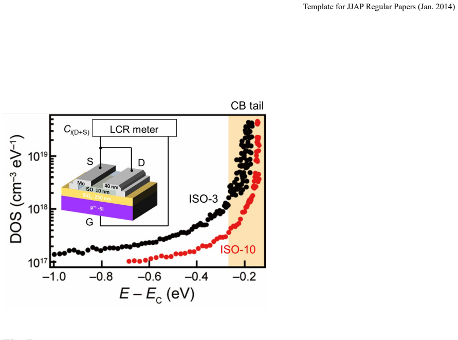
The central claim is that Si incorporation in amorphous InOx suppresses oxygen vacancies due to favorable bond energies, and that high Si concentrations reduce the activation energy and density of states, thereby decreasing trap density and allowing stable TFT operation under bias stresses, as evidenced by the inverse Meyer-Neldel rule indicating suitable ohmic contacts. A high-mobility bilayer TFT with homogeneous stacked channel further demonstrates the approach.
What carries the argument
Si selected as oxygen binder via bond-dissociation energy and Gibbs free energy to suppress unstable oxygen vacancies in the InOx TFT channel.
If this is right
- Activation energy and density of states decrease at high Si concentrations.
- Trap density is reduced in the TFT channel.
- Stable operation is realized under bias stresses.
- Inverse Meyer-Neldel rule appears, indicating reasonable ohmic contact.
- High-mobility bilayer TFT with homogeneous stacked channel is achieved.
Where Pith is reading between the lines
- Selecting dopants by thermodynamic binding strength could apply to vacancy control in other amorphous oxide semiconductors.
- The homogeneous stacked-channel design may simplify device fabrication compared to etch-stop-layer structures.
- Varying Si concentration offers a controlled system for testing models of carrier transport in disordered oxides.
- The vacancy-engineering approach could extend to improving long-term reliability in oxide-based electronics.
Load-bearing premise
That silicon binds oxygen more strongly than indium based on bond-dissociation energy and Gibbs free energy, allowing it to suppress unstable oxygen vacancies.
What would settle it
Measurement showing no reduction in activation energy or density of states at high Si concentrations, or continued bias-stress instability in high-Si InOx TFTs.
Figures


read the original abstract
Amorphous oxide semiconductors, especially indium oxide-based (InOx) thin-films, have been major candidates for high mobility with easy-to-use device processability. As one of the dopants in InOx semiconductors, we proposed Si to design a thin-film transistor (TFT) channel. Because the suppression of unstable oxygen vacancies in InOx is crucial to maintaining the semiconducting behavior, Si was selected as a strong oxygen binder that is reasonably available for large production. In this review, we focus on the overall properties observed in Si-incorporated amorphous InOx TFTs in terms of bond-dissociation energy, Gibbs free energy, Si-concentration dependence of TFT properties, carrier transport mechanism, and bias stress instability. In comparing low and high doping densities, we found that the activation energy and density of states decreased at a high Si concentration in InOx TFTs, implying that the trap density was reduced. As a result, stable operation under bias stresses could be realized. Furthermore, the inverse Meyer-Neldel rule was observed in the highly Si-doped InOx TFT, indicating reasonable ohmic contact. Based on our fundamental knowledge of the Si-doped InOx film, we developed a high-mobility bilayer TFT with a homogeneous stacked channel that was different from a TFT with an etch stop layer structure. The TFT showed remarkably stable operation. With simple element components based on InOx, it is possible to systematically discuss vacancy engineering in terms of conduction properties.
Editorial analysis
A structured set of objections, weighed in public.
Referee Report
Summary. The manuscript reviews Si-incorporated amorphous indium oxide (InOx) thin-film transistors, proposing Si as a dopant selected for its strong oxygen-binding properties (via bond-dissociation energy and Gibbs free energy) to suppress unstable oxygen vacancies. It summarizes concentration-dependent TFT properties, reporting that high Si levels reduce activation energy and density of states (implying lower trap density and improved bias-stress stability), observes the inverse Meyer-Neldel rule indicating reasonable ohmic contact, and demonstrates a high-mobility bilayer TFT with a homogeneous stacked channel that exhibits stable operation.
Significance. If the reported trends in electrical properties with Si incorporation are robustly supported by data, the work contributes a systematic discussion of vacancy engineering in simple InOx-based amorphous semiconductors. This could inform dopant strategies for stable, high-mobility TFTs in large-area electronics, with the bilayer device example providing a practical implementation distinct from etch-stop-layer structures.
major comments (2)
- [Abstract (Si selection criteria)] The rationale for selecting Si (abstract, second sentence) invokes its bond-dissociation energy and Gibbs free energy as stronger than In-O to explain vacancy suppression, but supplies no numerical values, comparison table, or cited references for the energies. This premise is load-bearing for the causal link to reduced trap density at high Si concentrations.
- [Abstract (high Si concentration effects)] The claim that activation energy and density of states decrease at high Si concentration (abstract), implying reduced trap density, is central to the stability conclusions but lacks detail on data extraction methods, error analysis, or specific figures/tables showing the quantitative trends.
minor comments (1)
- [Abstract] The abstract refers to 'this review' and 'our fundamental knowledge'; clarifying the manuscript's scope relative to the authors' prior publications on InOx TFTs would aid readers.
Simulated Author's Rebuttal
We thank the referee for the constructive comments and positive overall assessment of our review on Si-incorporated amorphous InOx TFTs. We address each major comment below and will revise the manuscript accordingly to improve clarity, particularly in the abstract.
read point-by-point responses
-
Referee: [Abstract (Si selection criteria)] The rationale for selecting Si (abstract, second sentence) invokes its bond-dissociation energy and Gibbs free energy as stronger than In-O to explain vacancy suppression, but supplies no numerical values, comparison table, or cited references for the energies. This premise is load-bearing for the causal link to reduced trap density at high Si concentrations.
Authors: We agree that the abstract would benefit from more explicit support for the Si selection rationale. While the main text discusses the bond-dissociation energies and Gibbs free energies (with numerical comparisons to In-O and supporting references), the abstract itself does not include these details. We will revise the abstract to incorporate a brief citation or key numerical values where space allows, thereby strengthening the causal connection to vacancy suppression and trap density reduction. revision: yes
-
Referee: [Abstract (high Si concentration effects)] The claim that activation energy and density of states decrease at high Si concentration (abstract), implying reduced trap density, is central to the stability conclusions but lacks detail on data extraction methods, error analysis, or specific figures/tables showing the quantitative trends.
Authors: The abstract summarizes findings that are presented with supporting data in the main manuscript, including concentration-dependent plots of activation energy and density of states extracted from temperature-dependent measurements. We will revise the abstract to include explicit references to the relevant figures and sections detailing the extraction methods. We will also ensure error analysis is more prominently described in the main text if it requires additional clarification. revision: partial
Circularity Check
No significant circularity; experimental observations on trap reduction are independent measurements.
full rationale
The paper reports direct experimental results from fabricated Si-incorporated InOx TFTs, including measured activation energies, density of states, and bias stress stability at varying Si concentrations. The selection of Si is presented as a prior design choice based on thermodynamic considerations (bond-dissociation energy, Gibbs free energy), but this rationale is not used to derive or force the reported data trends by construction. No equations, fits, or self-citations reduce the central claims (e.g., reduced trap density at high Si) to inputs; the results stand as independent empirical findings. This is the typical non-circular case for an experimental materials paper.
Axiom & Free-Parameter Ledger
axioms (2)
- domain assumption Si has higher bond-dissociation energy with oxygen than indium, making it an effective oxygen binder to suppress vacancies.
- domain assumption Oxygen vacancies are the dominant source of instability and carrier generation in amorphous InOx.
Reference graph
Works this paper leans on
- [1]
- [2]
- [3]
- [4]
- [5]
- [6]
- [7]
- [8]
-
[9]
J. Liu, D. B. Buchholz, R. P . Chang, A. Facchetti, and T. J. Marks, Adv. Mater. 22, 2333 (2010)
work page 2010
- [10]
-
[11]
N. Joo Hyon, R. Seung Yoon, J. Sung Jin, K. Chang Su, S. Sung -Woo, P . D. Rack, K. Dong-Joo, and B. Hong Koo, IEEE Electron Device Lett. 31, 567 (2010)
work page 2010
-
[12]
H. K. Müller, Phys. Status Solidi B 27, 723 (1968)
work page 1968
- [13]
- [14]
-
[15]
G. Gonçalves, P . Barquinha, L. Pereira, N. Franco, E. Alves, R. Martins, and E. Fortunato, Electrochem. Solid-State Lett. 13, H20 (2010)
work page 2010
- [16]
-
[17]
M.-F. Lin, X. Gao, N. Mitoma, T. Kizu, W. Ou -Yang, S. Aikawa, T. Nabatame, and K. Tsukagoshi, AIP Adv. 5, 017116 (2015)
work page 2015
- [18]
- [19]
-
[20]
T. Miyasako, M. Senoo, and E. Tokumitsu, Appl. Phys. Lett. 86, 162902 (2005)
work page 2005
-
[21]
S. Y. Park, K. H. Ji, H. Y. Jung, J.-I. Kim, R. Choi, K. S. Son, M. K. Ryu, S. Lee, and J. K. Jeong, Appl. Phys. Lett. 100, 162108 (2012)
work page 2012
- [22]
-
[23]
T. Kizu, S. Aikawa, N. Mitoma, M. Shimizu, X. Gao, M.- F. Lin, T. Nabatame, and K. Tsukagoshi, Appl. Phys. Lett. 104, 152103 (2014)
work page 2014
-
[24]
N. L. Dehuff, E. S. Kettenring, D. Hong, H. Q. Chiang, J. F. Wager, R. L. Hoffman, C. H. Park, and D. A. Keszler, J. Appl. Phys. 97, 064505 (2005)
work page 2005
-
[25]
P . Barquinha, A. Pimentel, A. Marques, L. Pereira, R. Martins, and E. Fortunato, J. Non- Cryst. Solids 352, 1749 (2006)
work page 2006
- [26]
-
[27]
K. Kurishima, T. Nabatame , N. Mitoma, T. Kizu, S. Aikawa, K. Tsukagoshi, A. Ohi, T. Chikyow, and A. Ogura, J. Vac. Sci. Technol., B 36, 061206 (2018)
work page 2018
-
[28]
K. Kurishima, T. Nabatame, T. Kizu, N. Mitoma, K. Tsukagoshi, T. Sawada, A. Ohi, I. Yamamoto, T. Ohishi, T. Chikyow, and A. Ogura, ECS Trans. 75, 149 (2016)
work page 2016
- [29]
-
[30]
K. Ghaffarzadeh, A. Nathan, J. Robertson, S. Kim, S. Jeon, C. Kim, U. I. Chung, and J.- H. Lee, Appl. Phys. Lett. 97, 143510 (2010)
work page 2010
-
[31]
J. W. Hennek, J. Smith, A. Yan, M. G. Kim, W. Zhao, V. P . Dravid, A. Facchetti, and T. J. Template for JJAP Regular Papers (Jan. 2014) 42 Marks, J Am Chem Soc 135, 10729 (2013)
work page 2014
-
[32]
W. Ou-Yang, N. Mitoma, T. Kizu, X. Gao, M. -F. Lin, T. Nabatame, and K. Tsukagoshi, Appl. Phys. Lett. 105, 163503 (2014)
work page 2014
- [33]
-
[34]
J. Y. Choi, K. Heo, K. S. Cho, S. W. Hwang, J. Chung, S. Kim, B. H. Lee, and S. Y. Lee, Sci Rep 7, 15392 (2017)
work page 2017
- [35]
- [36]
-
[37]
H.-W. Park, B.-K. Kim, J.-S. Park, and K.-B. Chung, Appl. Phys. Lett. 102, 102102 (2013)
work page 2013
- [38]
-
[39]
T. Kizu, N. Mitoma, M. Miyanaga, H. Awata, T. Nabatame, and K. Tsukagoshi, J. Appl. Phys. 118, 125702 (2015)
work page 2015
-
[40]
J.-S. Park, K. Kim, Y.-G. Park, Y.-G. Mo, H. D. Kim, and J. K. Jeong, Adv. Mater. 21, 329 (2009)
work page 2009
- [41]
-
[42]
E. Fortunato, P . Barquinha, and R. Martins, Adv. Mater. 24, 2945 (2012)
work page 2012
-
[43]
J. S. Park, W.-J. Maeng, H.-S. Kim, and J.-S. Park, Thin Solid Films 520, 1679 (2012)
work page 2012
-
[44]
H. Jeon, S. Na, M. R. Moon, D. Jung, H. Kim, and H.- J. Lee, J. Electrochem. Soc. 158, H949 (2011)
work page 2011
-
[45]
T. Iwasaki, N. Itagaki, T. Den, H. Kumomi, K. Nomura, T. Kamiya, and H. Hosono, Appl. Phys. Lett. 90, 242114 (2007)
work page 2007
- [46]
-
[47]
H.-K. Noh, K. Chang, B. Ryu, and W.-J. Lee, Phys. Rev. B 84, 115205 (2011)
work page 2011
- [48]
- [49]
-
[50]
D. Kang, H. Lim, C. Kim, I. Song, J. Park, Y. Park, and J. Chung, Appl. Phys. Lett. 90, 192101 (2007)
work page 2007
-
[51]
W.-T. Chen, S.-Y. Lo, S.-C. Kao, H.-W. Zan, C.-C. Tsai, J.-H. Lin, C.-H. Fang, and C. -C. Lee, IEEE Electron Device Lett. 32, 1552 (2011)
work page 2011
- [52]
-
[53]
S.-Y. Sung, J. H. Choi, U. B. Han, K. C. Lee, J.-H. Lee, J.-J. Kim, W. Lim, S. J. Pearton, D. P . Norton, and Y.-W. Heo, Appl. Phys. Lett. 96, 102107 (2010)
work page 2010
- [54]
-
[55]
J. Park, S. Kim, C. Kim, S. Kim, I. Song, H. Yin, K. -K. Kim, S. Lee, K. Hong, J. Lee, J. Jung, E. Lee, K.-W. Kwon, and Y. Park, Appl. Phys. Lett. 93, 053505 (2008)
work page 2008
-
[56]
X. Gao, S. Aikawa, N. Mitoma, M.-F. Lin, T. Kizu, T. Nabatame, and K. Tsukagoshi, Appl. Phys. Lett. 105, 023503 (2014)
work page 2014
- [57]
- [58]
-
[59]
Y. Abe, N. Ishiyama, H. Kuno, and K. Adachi, J. Mater. Sci. 40, 1611 (2005)
work page 2005
- [60]
-
[61]
L. T. Yan and R. E. I. Schropp, Thin Solid Films 520, 2096 (2012)
work page 2096
-
[62]
R. K. Gupta, K. Ghosh, and P . K. Kahol, Appl. Surf. Sci. 255, 8926 (2009)
work page 2009
-
[63]
K. Tsukagoshi, J. Tanabe, I. Yagi, K. Shigeto, K. Yanagisawa, and Y. Aoyagi, J. Appl. Phys. 99, 064506 (2006)
work page 2006
-
[64]
Z. Hu, J. Zhang, X. Chen, S. Ren, Z. Hao, X. Geng, and Y. Zhao, Sol. Energy Mater. Sol. Template for JJAP Regular Papers (Jan. 2014) 43 Cells 95, 2173 (2011)
work page 2014
-
[65]
T. Takenobu, T. Takahashi, T. Kanbara, K. Tsukagoshi, Y. Aoyagi, and Y. Iwasa, Appl. Phys. Lett. 88, 033511 (2006)
work page 2006
-
[66]
P . T. Liu, C. H. Chang, and C. J. Chang, ECS Trans. 67, 9 (2015)
work page 2015
- [67]
-
[68]
P . Kuo, C. Chang, and P . Liu: 2018 IEEE Symposium on VLSI Technology, 2018, p. 21
work page 2018
-
[69]
D.-B. Ruan, P .-T. Liu, K.-J. Gan, Y.-C. Chiu, M.-C. Yu, T.-C. Chien, Y.-H. Chen, P .-Y. Kuo, and S. M. Sze, Thin Solid Films 666, 94 (2018)
work page 2018
- [70]
- [71]
-
[72]
R. D. Shannon, Acta Crystallogr. 32, 751 (1976)
work page 1976
- [73]
- [74]
-
[75]
P . F. Carcia, R. S. McLean, M. H. Reilly, and G. Nunes, Appl. Phys. Lett. 82, 1117 (2003)
work page 2003
- [76]
-
[77]
Luo: Comprehensive Handbook of Chemical Bond Energies (CRC Press, 2007) Chap
Y.-R. Luo: Comprehensive Handbook of Chemical Bond Energies (CRC Press, 2007) Chap. 14, p. 667
work page 2007
-
[78]
Luo: Comprehensive Handbook of Chemical Bond Energies (CRC Press, 2007) Chap
Y.-R. Luo: Comprehensive Handbook of Chemical Bond Energies (CRC Press, 2007) Chap. 16, p. 713
work page 2007
-
[79]
Luo: Comprehensive Handbook of Ch emical Bond Energies (CRC Press, 2007) Chap
Y.-R. Luo: Comprehensive Handbook of Ch emical Bond Energies (CRC Press, 2007) Chap. 9, p. 455
work page 2007
-
[80]
Y. Q. Jia, J. Solid State Chem. 95, 184 (1991)
work page 1991
discussion (0)
Sign in with ORCID, Apple, or X to comment. Anyone can read and Pith papers without signing in.