REVIEW 6 minor 1 cited by
Superconducting nanowire single-photon spectrometer exploiting cascaded photonic crystal cavities
T0 review · 0 major / 6 minor · reviewed 2026-08-14 · deepseek-v4-flash
Pith's one-line read Cascaded photonic-crystal cavities give photon counters a ~1 nm spectrum.
desk verdict A clean TCMT-driven design for a cascaded-cavity SNSPD spectrometer, backed by 2D and 3D full-wave simulations, with only minor acknowledged simplifications. read the letter →
The pith
A machine-rendered reading of the paper's core claim, the machinery that carries it, and where it could break.
The reading
What carries the argument
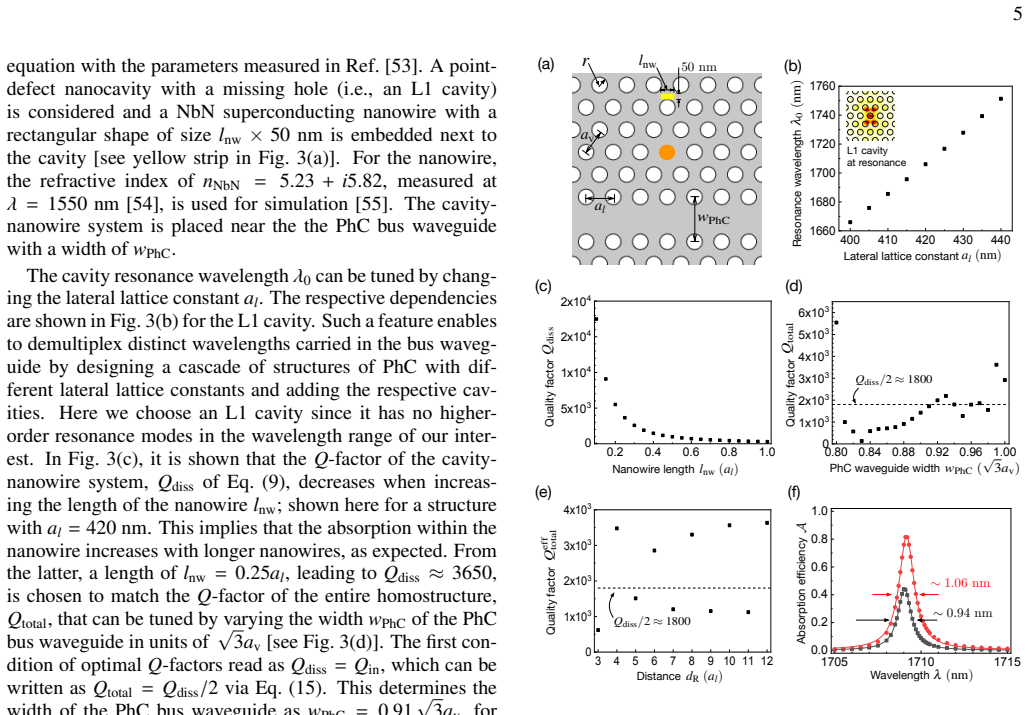
The central object is the side-coupled waveguide–cavity–nanowire building block described by temporal coupled-mode theory, with quality factors $Q_{\rm in}$ for waveguide–cavity coupling, $Q_{\rm diss}$ for the combined radiation and nanowire-absorption losses, and an effective input coupling $Q_{\rm in}^{\rm eff}$ that depends on the mirror phase $\theta=2\beta d_R+\Delta$. Setting $Q_{\rm diss}=Q_{\rm in}^{\rm eff}$ at the resonance of each cavity is what makes the reflected and cavity fields interfere so that nearly all light is dissipated, and cascading those blocks with different lattice constants demultiplexes wavelengths spatially. The Lorentzian absorption line shape yields the spectral resolution $\mathrm{FWHM}_\lambda\approx \lambda_0^{\rm eff}/Q_{\rm total}$.
What would settle it
Fabricate a two-cavity 3D device and record the absorption spectrum for input pulses whose temporal width is comparable to the device length; if the peaks deviate from Lorentzian shapes or the peak absorption falls well below 80%, the single-mode and long-pulse assumption behind the optimized conditions is the cause. A simpler numerical check is to run a full-wave simulation with the mirror distance $d_R$ made large, where the paper itself notes the Lorentzian prediction is no longer expected to hold.
Extended reading notes
Core claim
The central claim is that cascading side-coupled photonic-crystal cavities with distinct resonance wavelengths in front of superconducting nanowires yields a single-photon spectrometer with absorption efficiencies around 80% and spectral resolution around 1 nm. For one cavity–nanowire building block the paper derives from temporal coupled-mode theory that absorption is maximized at critical coupling, $Q_{\rm in}=Q_{\rm diss}$, but cannot exceed 50%. Attaching a far-detuned photonic-crystal mirror at the end of the bus waveguide creates coherent perfect absorption, and the modified condition $Q_{\rm diss}=Q_{\rm in}^{\rm eff}$ pushes total dissipation toward unity while the fraction absorbed in the nanowire grows with $Q_c/Q_{\rm nw}$. The paper verifies these conditions by full-wave simulation: four cascaded cavities in two dimensions absorb 74–84% per channel with about 1 nm linewidth, and two cascaded L3 cavities in a three-dimensional slab reach about 80% with similar resolution.
Load-bearing premise
Everything rests on the assumption that a single mode carries the light down the bus waveguide and that the incoming pulse is long enough to be treated as a steady wave; if reflections at the joints between photonic-crystal sections or short pulses excite additional modes, the optimal coupling conditions and the predicted 80% absorption need not hold.
Editorial extensions
If this is right
- A fabricated 2D device with four cascaded cavities should assign 74–84% of each wavelength channel to its own nanowire, with crosstalk in neighboring nanowires below 0.2%.
- Terminating the bus waveguide with a far-detuned photonic-crystal mirror is the element that lifts per-channel absorption above 50% and toward the theoretical unit ceiling.
- In a 3D slab geometry the same design reaches about 80% absorption with two cascaded channels, so the mechanism is not an artifact of the 2D approximation.
- Spectral resolution near 1 nm is set by the total quality factor, giving a direct design trade-off: longer nanowires absorb more but broaden the line, while higher cavity $Q$ sharpens the line and improves absorption.
Reading between the lines
- Beyond the paper: the same cascade could be built with a constant lattice constant by tuning each cavity's resonance through local hole shifts or radii, a route the paper mentions only as an alternative and one that would remove heterointerface reflections entirely.
- Beyond the paper: the Fabry–Pérot peak the simulations show near 1529 nm suggests that optimizing the input access waveguide should further flatten the channel response, a step the paper leaves for future work.
- Beyond the paper: a direct experimental check of the line shape under short pulses would test the single-mode and long-pulse assumption on which the optimized conditions rest.
- Beyond the paper: if the mirror phase alone can tune $Q_{\rm in}^{\rm eff}$, one might make the spectrometer reconfigurable by moving or adjusting the mirror, reallocating efficiency and resolution without changing the cavities.
Signed reviews
Editorial analysis
A structured set of objections, weighed in public.
Referee Report
Summary. This paper proposes an on-chip single-photon spectrometer based on cascaded photonic crystal cavities side-coupled to a photonic crystal bus waveguide, with superconducting nanowires placed adjacent to each cavity. Using temporal coupled-mode theory, the authors derive three design conditions for high absorption efficiency and fine spectral resolution: critical coupling between waveguide and cavity (Q_diss = Q_in), a high cavity quality factor relative to the nanowire absorption (Q_c >> Q_nw), and a large total quality factor for a narrow linewidth. They further show that a terminating mirror lifts the 50% upper bound on total dissipation, enabling absorption efficiencies up to unity in the absence of loss. Full-wave COMSOL simulations in 2D for four cascaded L1 cavities give absorption efficiencies of 74–84% with a FWHM of about 1 nm; 3D slab simulations for two cascaded L3 cavities give about 80% absorption with FWHMs between 0.64 nm and 0.99 nm, and negligible crosstalk. The paper acknowledges the single-mode limitation of the TCMT formalism (footnote [52]), the fixed NbN refractive index (footnote [55]), and the computational restriction to two 3D cavities.
Significance. The proposed design addresses a genuine need in integrated quantum photonics: adding spectral resolution to superconducting nanowire single-photon detectors. If the simulated performance is realized in experiments, the device would offer a compact, wavelength-multiplexed alternative to grating-based on-chip spectrometers, with potential application to multicolor entangled light and quantum white-light interferometry. The paper's strengths include a parameter-free TCMT derivation, independent full-wave validation of the predicted absorption and linewidth, explicit crosstalk estimates, and open discussion of the main simplifications. The mirror concept is correctly attributed to prior work (ref. [44]). The final performance numbers come from the full-wave simulations themselves, not from the TCMT, so the acknowledged single-mode limitation of the analytical model does not undermine the central claim.
minor comments (6)
- [Figure 5 caption] The caption states "with (black curve) and without (red curve) the PhC mirror," whereas the main text and the red circles/black squares in the figure indicate the opposite color assignment; please correct the caption or the text for consistency.
- [Section IV.B] The chosen waveguide width wPhC = 0.66√3av yields Qtotal ≈ 1390, which deviates from the stated critical-coupling condition Qtotal = Qdiss/2 ≈ 1700 shown in Fig. A2(b); since the text calls the structure "moderately optimized," please quantify this deviation and explain why the 80% absorption is nonetheless obtained.
- [Footnote [55]] The fixed NbN refractive index measured at 1550 nm is used for resonances near 1670–1710 nm in 2D and 1530–1535 nm in 3D, although nNbN varies with wavelength; a short discussion of the expected impact on Q-factor matching and resonance positions would strengthen the design claims.
- [Footnote [52]] Footnote [52] correctly limits the TCMT model to the single-mode regime; because the final absorption values come from full-wave simulations, this is not an obstacle to the central claim, but the main text could state more explicitly that the TCMT is used only for parameter selection and that the simulations incorporate multi-mode effects at the heterointerfaces.
- [Section IV] "Waveoptics module" should read "Wave Optics module"; also, the phrase "the measured wavelength range" in Section IV.B appears to refer to simulated rather than measured data.
- [Figure 3(d)] The axis label uses √3av while the caption says the width is given in units of √3al; since av = 400 nm and al = 420 nm, please make the notation consistent throughout the figure and text.
Circularity Check
No circularity: the TCMT-derived conditions are used only to choose structural parameters, while the central efficiency and resolution claims come from independent full-wave simulations.
full rationale
The paper's derivation chain is self-contained with respect to its central claim. In Sec. III, temporal coupled-mode theory is used to derive optimal Q-factor conditions such as Q_diss = Q_in^eff, starting from an independent analytical framework (refs. [44], [45]). These conditions are then used in Sec. IV and Appendix B only to select structural parameters (nanowire length, waveguide width, mirror distance). The reported absorption efficiencies of about 80% and FWHMs of about 1 nm are obtained from full-wave COMSOL simulations that solve Maxwell's equations, not by re-inserting TCMT outputs into the same model. Lorentzian fitting is used only to read off resonance positions and widths from the simulated spectra; it is a data-reduction step, not a fitted input that generates the claimed efficiency. The mirror enhancement mechanism is attributed to prior work on coherent perfect absorption (ref. [44]) and is applied rather than redefined in terms of this paper's own data. The only self-citations (e.g., ref. [17] for context on SNSPDs in photonic-crystal cavities) are background references and are not load-bearing for the derivation. Footnote [52] candidly states the single-mode approximation limitation, which is a correctness caveat rather than evidence of circularity. No fitted parameter is renamed as a prediction, and no uniqueness or ansatz is imported from same-author prior work to force the result. The central numerical claims are therefore independently verified rather than circularly constructed.
Assumptions & free parameters
free parameters (8)
- Nanowire length in 2D structures (lnw) =
0.25 a_l (about 105 nm for a_l = 420 nm)
- PhC bus waveguide width in 2D (w_PhC) =
0.91 sqrt(3) a_v (with a_v = 400 nm)
- Mirror distance in 2D (d_R) =
5 a_l (2.1 um)
- Nanowire length in 3D (lnw) =
2 a_l
- PhC waveguide width in 3D (w_PhC) =
0.66 sqrt(3) a_v
- Mirror distance in 3D (d_R) =
10 a_l
- Nearest-neighbor hole shift in L3 cavity (s) =
0.2 a_l
- Lateral lattice constants for cascaded channels =
2D: 420, 415, 410, 405, 400 nm; 3D: 420 and 418 nm
assumptions (5)
- domain assumption Single-mode approximation in temporal coupled-mode theory
- domain assumption The PhC mirror acts as an ideal reflector with a wavelength-independent phase
- domain assumption The superconducting nanowire is modeled as a simple rectangular loss channel with constant complex refractive index
- domain assumption Light is injected in the fundamental TE-like guided mode
- domain assumption No absorption or scattering loss in the silicon photonic crystal itself
Cite this review
Pith. "Pith review of Superconducting nanowire single-photon spectrometer exploiting cascaded photonic crystal cavities." pith.science (2026). https://pith.science/paper/RNMUZN6G
@misc{pith2026190801681,
  author       = {Pith},
  title        = {Pith review of: Superconducting nanowire single-photon spectrometer exploiting cascaded photonic crystal cavities},
  year         = {2026},
  howpublished = {\url{https://pith.science/paper/RNMUZN6G}},
  note         = {Machine review of arXiv:1908.01681}
}
read the original abstract
Superconducting nanowire single-photon detectors promise efficient (~100%) and fast (~Gcps) detection of light at the single-photon level. They constitute one of the building blocks to realize integrated quantum optical circuits in a waveguide architecture. The optical response of single-photon detectors, however, is limited to measure only the presence of photons. It misses the capability to resolve the spectrum of a possible broadband illumination. In this work, we propose the optical design for a superconducting nanowire single-photon spectrometer in an integrated optical platform. We exploit a cascade of cavities with different resonance wavelengths side-coupled to a photonic crystal bus waveguide. This allows to demultiplex different wavelengths into different spatial regions, where individual superconducting nanowires that measure the presence of single photons are placed next to these cavities. We employ temporal coupled-mode theory to derive the optimal conditions to achieve a high absorption efficiency in the nanowire with fine spectral resolution. It is shown that the use of a mirror at the end of the cascaded system that terminates the photonic crystal bus waveguide increases the absorption efficiency up to unity, in principle, in the absence of loss. The expected response is demonstrated by full-wave simulations for both two-dimensional and three-dimensional structures. Absorption efficiencies of about 80% are achieved both in two-dimensional structures for four cascaded cavities and in three-dimensional structures for two cascaded cavities. The achieved spectral resolution is about 1 nm. We expect that the proposed setup, both analytically studied and numerically demonstrated in this work, offers a great impetus for future quantum nanophotonic on-chip technologies.
Figures


Figures from the paper (3 more)


Forward citations
Cited by 1 Pith paper
-
Chip-based measurement-device-independent quantum key distribution
A demonstration of measurement-device-independent quantum key distribution using monolithically integrated indium phosphide transmitters, with asymptotic secure key rates up to 200 km and a predicted range beyond 350 km.
Reference graph
Works this paper leans on
-
[52]
K. Bogumil, J. Orphal, T. Homann, S. V oigt, P. Spietz, O. C. Fleischmann, A. V ogel, M. Hartmann, H. Kromminga, H. Bovensmann, J. Frerick, and J. P. Burrows, “Measurements of molecular absorption spectra with the sciamachy pre-flight model: instrument characterization and reference data for at- mospheric remote-sensing in the 230–2380 nm region,” Jour- na...
work page 2003
-
[55]
Efficiently coupling light to superconducting nanowire single-photon detectors,
X. Hu, C. W. Holzwarth, D. Masciarelli, E. A. Dauler, and K. K. Berggren, “Efficiently coupling light to superconducting nanowire single-photon detectors,” IEEE Trans. Appl. Super- cond. 19, 336 (2009)
work page 2009
-
[44]
Large-scale integration of wavelength-addressable all-optical memories on a photonic crystal chip,
E. Kuramochi, K. Nozaki, A. Shinya, K. Takeda, T. Sato, S. Matsuo, H. Taniyama, H. Sumikura, and M. Notomi, “Large-scale integration of wavelength-addressable all-optical memories on a photonic crystal chip,” Nat. Photon. 8, 474 (2014)
work page 2014
-
[1]
Single-photon detectors for optical quantum information applications,
R. H. Hadfield, “Single-photon detectors for optical quantum information applications,” Nature Photonics 3, 696 (2009)
work page 2009
-
[2]
(7) One can see that the absorptionA cannot be greater than 50% since light extraction from the bus waveguide to the cavity is limited to maximally 50%. Such upper bound can also be explained by looking at the extent to which light is neither transmitted nor reflected, i.e., the total dissipationD =A +L, whereL =|l|2, written as D = 1 Qdiss 1 2Qin ⏐⏐⏐⏐i ( ...
work page 2000
-
[3]
Invited review article: Single-photon sources and detectors,
M. D. Eisaman, A. Migdall J. Fan, and S. V . Polyakov, “Invited review article: Single-photon sources and detectors,” Rev. Sci. Instrum. 82, 071101 (2011)
work page 2011
-
[4]
Quantum cryptography,
N. Gisin, G. Ribordy, W. Tittel, and H. Zbinden, “Quantum cryptography,” Rev. Mod. Phys.74, 145 (2002)
2002
-
[5]
A scheme for e ffi- cient quantum computation with linear optics,
E. Knill, R. Laflamme, and G. J. Milburn, “A scheme for e ffi- cient quantum computation with linear optics,” Nature 409, 46 (2001)
work page 2001
Show all 65 references
-
[6]
Linear optical quantum computing with photonic qubits,
P. Kok, W. J. Munro, K. Nemoto, T. C. Ralph, J. P. Dowling, and G. J. Milburn, “Linear optical quantum computing with photonic qubits,” Rev. Mod. Phys.79, 135 (2007)
2007
-
[7]
Quantum imaging,
L. A. Lugiato, A. Gatti, and E. Brambilla, “Quantum imaging,” J. Opt. B: Quantum Semiclass. Opt. 4, S176 (2002)
2002
-
[8]
Advances in photonic quantum sensing,
S. Pirandola, B. R. Bardhan, T. Gehring, C. Weedbrook, and S. Lloyd, “Advances in photonic quantum sensing,” Nat. Pho- ton. 12, 724 (2018)
2018
-
[9]
Picosecond superconducting single- photon optical detector,
G. N. Gol’tsman, O. Okunev, G. Chulkova, A. Lipatov, A. Se- menov, K. Smirnov, B. V oronov, A. Dzardanov, C. Williams, and R. Sobolewski, “Picosecond superconducting single- photon optical detector,” Applied Physics Letters 79, 705 (2001)
2001
-
[10]
Detection effi- ciency of large-active-area NbN single-photon superconducting detectors in the ultraviolet to near-infrared range,
A. Verevkin, J. Zhang, and Roman Sobolewski, “Detection effi- ciency of large-active-area NbN single-photon superconducting detectors in the ultraviolet to near-infrared range,” Appl. Phys. Lett. 80, 4687 (2002)
2002
-
[11]
Nanowire single-photon detector with an integrated optical cavity and anti-reflection coating,
K. M. Rosfjord, J. K. W. Yang, E. A. Dauler, A. J. Kerman, V . Anant, B. M. V oronov, G. N. Gol’tsman, and Karl K. Berggren, “Nanowire single-photon detector with an integrated optical cavity and anti-reflection coating,” Opt. Express14, 527 (2006)
2006
-
[12]
Photon-number-resolution with sub-30-ps timing using multi- element superconducting nanowire single photon detectors,
E. A. Dauler, A. J. Kerman, B. S. Robinson, J. K. W. Yang, B. V oronov, G. Gol’tsman, S. A. Hamilton, and K. K. Berggren, “Photon-number-resolution with sub-30-ps timing using multi- element superconducting nanowire single photon detectors,” J. Mod. Opt. 56, 364 (2009)
2009
-
[13]
Waveguide supercon- ducting single-photon detectors for integrated quantum pho- tonic circuits,
J. P. Sprengers, A. Gaggero, D. Sahin, S. Jahanmirinejad, G. Frucci, F. Mattioli, R. Leoni, J. Beetz, M. Lermer, M. Kamp, S. H ¨ofling, R. Sanjines, and A. Fiore, “Waveguide supercon- ducting single-photon detectors for integrated quantum pho- tonic circuits,” Appl. Phys. Lett....
2011
-
[14]
Waveguide-integrated superconducting nanowire single-photon detectors,
S. Ferrari, C. Schuck, and W. Pernice, “Waveguide-integrated superconducting nanowire single-photon detectors,” Nanopho- tonics 7, 1725 (2018)
2018
-
[15]
Fully integrated quantum photonic circuit with an electrically driven light source,
S. Khasminskaya, F. Pyatkov, K. Słowik, S. Ferrari, O. Kahl, V . Kovalyuk, P. Rath, A. Vetter, F. Hennrich, M. M. Kappes, G. Gol’tsman, A. Korneev, C. Rockstuhl, R. Krupke, and W. H. P. Pernice, “Fully integrated quantum photonic circuit with an electrically driven light sourc...
2016
-
[16]
Waveguide in- tegrated superconducting single-photon detectors implemented as near-perfect absorbers of coherent radiation,
M. K. Akhlaghi, E. Schelew, and J. F. Young, “Waveguide in- tegrated superconducting single-photon detectors implemented as near-perfect absorbers of coherent radiation,” Nat. Commun. 6, 8233 (2015)
2015
-
[17]
Cavity-enhanced and ultrafast superconduct- ing single-photon detectors,
A. Vetter, S. Ferrari, P. Rath, R. Alaee, O. Kahl, V . Kovalyuk, S. Diewald, G. N. Goltsman, A. Korneev, C. Rockstuhl, and W. H. P. Pernice, “Cavity-enhanced and ultrafast superconduct- ing single-photon detectors,” Nano Letters 16, 7085 (2016)
2016
-
[18]
Superconducting nanowire single-photon detector implemented in a 2D photonic crystal cavity,
J. M ¨unzberg, A. Vetter, F. Beutel, W. Hartmann, S. Fer- rari, W. H. P. Pernice, and C. Rockstuhl, “Superconducting nanowire single-photon detector implemented in a 2D photonic crystal cavity,” Optica5, 658 (2018)
2018
-
[19]
Detection mechanism of superconducting nanowire single-photon detec- tors,
A. Engel, J. J. Renema, K. Il’in, and A. Semenov, “Detection mechanism of superconducting nanowire single-photon detec- tors,” Supercond. Sci. Technol.28, 114003 (2015)
2015
-
[20]
Universal response curve for nanowire superconducting single-photon detectors,
J. J. Renema, G. Frucci, Z. Zhou, F. Mattioli, A. Gaggero, R. Leoni, M. J. A. de Dood, A. Fiore, and M. P. van Ex- ter, “Universal response curve for nanowire superconducting single-photon detectors,” Phys. Rev. B87, 174526 (2013)
2013
-
[21]
Discrete tunable color entanglement,
S. Ramelow, L. Ratschbacher, A. Fedrizzi, N. K. Langford, and A. Zeilinge, “Discrete tunable color entanglement,” Phys. Rev. Lett. 103, 253601 (2009)
2009
-
[22]
Generalized multiphoton quantum interference,
M. Tillmann, S.-H. Tan, S. E. Stoeckl, B. C. Sanders, H. de Guise, R. Heilmann, S. Nolte, A. Szameit, and P. Walther, “Generalized multiphoton quantum interference,” Phys. Rev. X 5, 041015 (2015)
2015
-
[23]
Quantum enhancement of accuracy and precision in optical interferometry,
F. Kaiser, P. Vergyris, D. Aktas, C. Babin, L. Labont ´e, and S. Tanzilli, “Quantum enhancement of accuracy and precision in optical interferometry,” Light: Sci. & Appl.7, 17163 (2018)
2018
-
[24]
Spectrally multiplexed single-photon detection with hybrid superconducting nanophotonic circuits,
O. Kahl, S. Ferrari, V . Kovalyuk, A. Vetter, G. Lewes- Malandrakis, C. Nebel, A. Korneev, G. Goltsman, and Wol- fram Pernice, “Spectrally multiplexed single-photon detection with hybrid superconducting nanophotonic circuits,” Optica 4, 557 (2017)
2017
-
[25]
Broadband on-chip single-photon spectrometer,
R. Cheng, C.-L. Zou, X. Guo, S. Wang, X. Han, and H. X. Tang, “Broadband on-chip single-photon spectrometer,” arXiv:1908.00824
1908 arXiv
-
[26]
Photonic quan- tum technologies,
J. L. O’Brien, A. Furusawa, and J. Vucˇckovi´c, “Photonic quan- tum technologies,” Nat. Photon. 3, 687 (2009)
2009
-
[27]
Quan- tum dots in photonic crystals: From quantum information processing to single photon nonlinear optics,
D. Englund, I. Fushman, A. Faraon, and J. Vu ˇckovi´c, “Quan- tum dots in photonic crystals: From quantum information processing to single photon nonlinear optics,” Photonics and Nanostructures – Fundamentals and Applications 7, 56 (2009). 11
2009
-
[28]
Photonic crystal microcavities for cavity quantum electrodynamics with a single quantum dot,
J. Vu ˇckovi´c and Y . Yamamoto, “Photonic crystal microcavities for cavity quantum electrodynamics with a single quantum dot,” Appl. Phys. Lett. 82, 2374 (2003)
2003
-
[29]
Con- trolling the spontaneous emission rate of single quantum dots in a two-dimensional photonic crystal,
D. Englund, D. Fattal, E. Waks, G. Solomon, B. Zhang, T. Nakaoka, Y . Arakawa, Y . Yamamoto, and J. Vuˇckovi´c, “Con- trolling the spontaneous emission rate of single quantum dots in a two-dimensional photonic crystal,” Phys. Rev. Lett. 95, 013904 (2005)
2005
-
[30]
Controlling cavity reflectivity with a single quan- tum dot,
D. Englund, A. Faraon, I. Fushman, N. Stoltz, P. Petro ff, and J. Vuˇckovi´c, “Controlling cavity reflectivity with a single quan- tum dot,” Nature 450, 857 (2007)
2007
-
[31]
Generation and transfer of single photons on a photonic crystal chip,
D. Englund, A. Faraon, B. Zhang, Y . Yamamoto, and J. Vuˇckovi´c, “Generation and transfer of single photons on a photonic crystal chip,” Opt. Exp. 15, 5550 (2007)
2007
-
[32]
Generation and manipulation of nonclassical light using pho- tonic crystals,
J. Vuckovic, D. Englund, D. Fattal, E. Waks, and Y . Yamamoto, “Generation and manipulation of nonclassical light using pho- tonic crystals,” Physica E: Low- Dimension. Sys. Nanostruct. 32, 466 (2006)
2006
-
[33]
Single-photon non-linear optics with a quantum dot in a waveguide,
A. Javadi, I. S ¨ollner, M. Arcari, S. Lindskov Hansen, L. Mi- dolo, S. Mahmoodian, G. Kir ˇsansk˙e, T. Pregnolato, E. H. Lee, J. D. Song, S. Stobbe, and P. Lodahl, “Single-photon non-linear optics with a quantum dot in a waveguide,” Nature Communi- cations 6, 8655 (2015)
2015
-
[34]
Subwavelength vacuum lattices and atom–atom interactions in two-dimensional photonic crystals,
A. Gonz ´alez-Tudela, C.-L. Hung, D. E. Chang, J. I. Cirac, and H. J. Kimble, “Subwavelength vacuum lattices and atom–atom interactions in two-dimensional photonic crystals,” Nature Pho- tonics 9, 320 (2015)
2015
-
[35]
Two- dimensional photonic crystals for engineering atom-light inter- actions,
S.-P. Yu, J. A. Muniz, C.-L. Hung, and H. J. Kimble, “Two- dimensional photonic crystals for engineering atom-light inter- actions,” PNAS116, 12743 (2019)
2019
-
[36]
Chiral quan- tum optics,
P. Lodahl, S. Mahmoodian, S. Stobbe, A. Rauschenbeutel, P. Schneeweiss, J. V olz, H. Pichler, and P. Zoller, “Chiral quan- tum optics,” Nature 541, 473 (2017)
2017
-
[37]
Highly ef- ficient in-plane channel drop filter in a two-dimensional het- erophotonic crystal,
H. Takano, B.-S. Song, T. Asano, and S. Noda, “Highly ef- ficient in-plane channel drop filter in a two-dimensional het- erophotonic crystal,” Appl. Phys. Lett. 86, 241101 (2005)
2005
-
[38]
Multichannel add/drop filter based on in-plane hetero photonic crystals,
B.-S. Song, T. Asano, Y . Akahane, Y . Tanaka, and S. Noda, “Multichannel add/drop filter based on in-plane hetero photonic crystals,” J. Light. Technol.23, 1449 (2005)
2005
-
[39]
Highly e ffi- cient multi-channel drop filter in a two-dimensional hetero pho- tonic crystal,
H. Takano, B.-S. Song, T. Asano, and S. Noda, “Highly e ffi- cient multi-channel drop filter in a two-dimensional hetero pho- tonic crystal,” Opt. Express 14, 3491 (2006)
2006
-
[40]
High transmission through sharp bends in photonic crystal waveguides,
A. Mekis, J. C. Chen, I. Kurland, S. Fan, P. R. Villeneuve, and J. D. Joannopoulos, “High transmission through sharp bends in photonic crystal waveguides,” Phys. Rev. Lett.77, 3787 (1996)
1996
-
[41]
Extremely large group-velocity dispersion of line-defect waveguides in photonic crystal slabs,
M. Notomi, K. Yamada, A. Shinya, J. Takahashi, C. Takahashi, and I. Yokohama, “Extremely large group-velocity dispersion of line-defect waveguides in photonic crystal slabs,” Phys. Rev. Lett. 87, 253902 (2001)
2001
-
[42]
Coupling light in photonic crystal waveguides: A review,
H. S. Dutta, A. K. Goyal, V . Srivastava, and S. Pal, “Coupling light in photonic crystal waveguides: A review,” Photonics and Nanostructures – Fundamentals and Applications20, 41 (2016)
2016
-
[43]
High-Q pho- tonic nanocavity in a two-dimensional photonic crystal,
Y . Akahane, T. Asano, B.-S. Song, and S. Noda, “High-Q pho- tonic nanocavity in a two-dimensional photonic crystal,” Nature 425, 944 (2003)
2003
-
[45]
Role of inter- faces in heterophotonic crystals for manipulation of photons,
B.-S. Song, T. Asano, Y . Akahane, and S. Noda, “Role of inter- faces in heterophotonic crystals for manipulation of photons,” Phys. Rev. B 71, 195101 (2005)
2005
-
[46]
Temporal coupled- mode theory for the fano resonance in optical resonators,
S. Fan, W. Suh, and J. D. Joannopoulos, “Temporal coupled- mode theory for the fano resonance in optical resonators,” J. Opt. Soc. Am. A 20, 569 (2003)
2003
-
[47]
(1) and (2)
The absence of a factor of √ 2 in the coupling terms can be explained when comparing it to the other coupling terms given in Eqs. (1) and (2). Because the fields Erad and Enw are con- sidered to be the superposed field of right- and left-propagating waves with the normalization ...
-
[48]
Optical microsphere res- onators: optimal coupling to high-q whispering-gallery modes,
M. L. Gorodetsky and V . S. Ilchenko, “Optical microsphere res- onators: optimal coupling to high-q whispering-gallery modes,” J. Opt. Soc. Am. B 16, 147 (1999)
1999
-
[49]
Observation of criti- cal coupling in a fiber taper to a silica-microsphere whispering- gallery mode system,
M. Cai, O. Painter, and K. J. Vahala, “Observation of criti- cal coupling in a fiber taper to a silica-microsphere whispering- gallery mode system,” Phys. Rev. Lett.85, 74 (2000)
2000
-
[50]
Critical coupling and its control in optical waveguide-ring resonator systems,
A. Yariv, “Critical coupling and its control in optical waveguide-ring resonator systems,” IEEE Photonics Technol. Lett. 14, 483 (2002)
2002
-
[51]
Coherent perfect absorbers: Time-reversed lasers,
Y . D. Chong, Li Ge, H. Cao, and A. D. Stone, “Coherent perfect absorbers: Time-reversed lasers,” Phys. Rev. Lett.105, 053901 (2010)
2010
-
[53]
As a remark, it is also worth to note that the formalism we use is valid only when the single-mode approximation holds or equiv- alently the temporal width of a propagating wave is extremely long with respect to the size of the whole structure. The formal- ism is thus not vali...
-
[54]
Infrared refractive indexes of sil- icon germanium and modified selenium glass,
C. D Salzberg and J. J Villa, “Infrared refractive indexes of sil- icon germanium and modified selenium glass,” J. Opt. Soc. A. 47, 244 (1957)
1957
-
[56]
For simplicity, a fixed value of nNbN mea- sured atλ = 1550 nm is used in the whole range of wavelength considered in this work
The nNbN varies with the wavelength, e..g, nNbN = 5.62 + i6.14 atλ = 1750 nm [54]. For simplicity, a fixed value of nNbN mea- sured atλ = 1550 nm is used in the whole range of wavelength considered in this work
-
[57]
Fine-tuned high-Q photonic-crystal nanocavity,
Y . Akahane, T. Asano, B.-S. Song, and S. Noda, “Fine-tuned high-Q photonic-crystal nanocavity,” Opt. Express 13, 1202 (2005)
2005
-
[58]
Systematic hole-shifting of l- type nanocavity with an ultrahigh q factor,
E. Kuramochi, El. Grossman, K. Nozaki, K. Takeda, A. Shinya, H. Taniyama, and M. Notomi, “Systematic hole-shifting of l- type nanocavity with an ultrahigh q factor,” Opt. Express 39, 5780 (2014)
2014
-
[59]
Resonant- wavelength control of nanocavities by nanometer-scaled ad- justment of two-dimensional photonic crystal slab structures,
B.-S. Song, T. Nagashima, T. Asano, and S. Noda, “Resonant- wavelength control of nanocavities by nanometer-scaled ad- justment of two-dimensional photonic crystal slab structures,” IEEE Photonics Tech. Lett. 20, 532 (2008)
2008
-
[60]
Structural dependence of coupling between a two-dimensional photonic crystals waveguide and a wire waveguide,
E. Miyai and S. Noda, “Structural dependence of coupling between a two-dimensional photonic crystals waveguide and a wire waveguide,” J. Opt. Soc. Amer. B, Opt. Phys. 21, 67 (2004)
2004
-
[61]
Active control of slow light on a chip with photonic 12 crystal waveguide,
Y . A. Vlasv, M. O’Boyle, H. F. Hamann, S. J. McNab, and N. Moll, “Active control of slow light on a chip with photonic 12 crystal waveguide,” Nature438, 66 (2005)
2005
-
[62]
Linewidth narrowing and pur- cell enhancement in photonic crystal cavities on an er-doped silicon nitride platform,
Y . Gong, M. Makarova, S. Yerci, R. Li, M. J. Stevens, B. Baek, S. W. Nam, R. H. Hadfield, S. N. Dorenbos, V . Zwiller, J. Vuˇckovi´c, and L. Dal Negro, “Linewidth narrowing and pur- cell enhancement in photonic crystal cavities on an er-doped silicon nitride platform,” Opt. Ex...
2010
-
[63]
These values are much smaller than the Q-factors of L1 (s=0.2), L3 (s=0.2), and L5 (s=0.25) cavities on air substrate, which are 3975, 93046, and 114856, respectively
We have calculated the Q-factors of L1 (with the shift of s=0.2), L3 (s =0.2), and L5 (s =0.25) cavities on SiO 2 substrate and they are 771, 983, and 2356, respectively. These values are much smaller than the Q-factors of L1 (s=0.2), L3 (s=0.2), and L5 (s=0.25) cavities on ai...
-
[64]
Slow light in photonic crystals,
T. Baba, “Slow light in photonic crystals,” Nat. Photon. 2, 465 (2008)
2008
-
[65]
J. D. Joannopoulos, R. D. Meade, J. N. Winn, and S. G. John- son, Photonic Crystals: Molding the Flow of Light (Princeton University Press, 1995)
1995
Reviewed August 14, 2026 · model on record in the stance chip above.
Discussion (0). Continue with ORCID to comment.