REVIEW 3 major objections 3 minor 33 references
Electric selective activation of memristive interfaces in TaO$_x$-based devices
T0 review · 3 major / 3 minor · reviewed 2026-08-14 · deepseek-v4-flash
Pith's one-line read A single TaOx memristive device can be made to switch between clockwise and counter-clockwise resistance loops simply by choosing the voltage excursion asymmetry.
desk verdict Solid experimental demonstration of protocol-tunable loop circulation in a single TaOx device; the mechanistic model is fitted rather than predictive, and a missing control leaves the two-interface story underdetermined. read the letter →
The pith
A machine-rendered reading of the paper's core claim, the machinery that carries it, and where it could break.
The reading
What carries the argument
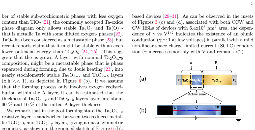
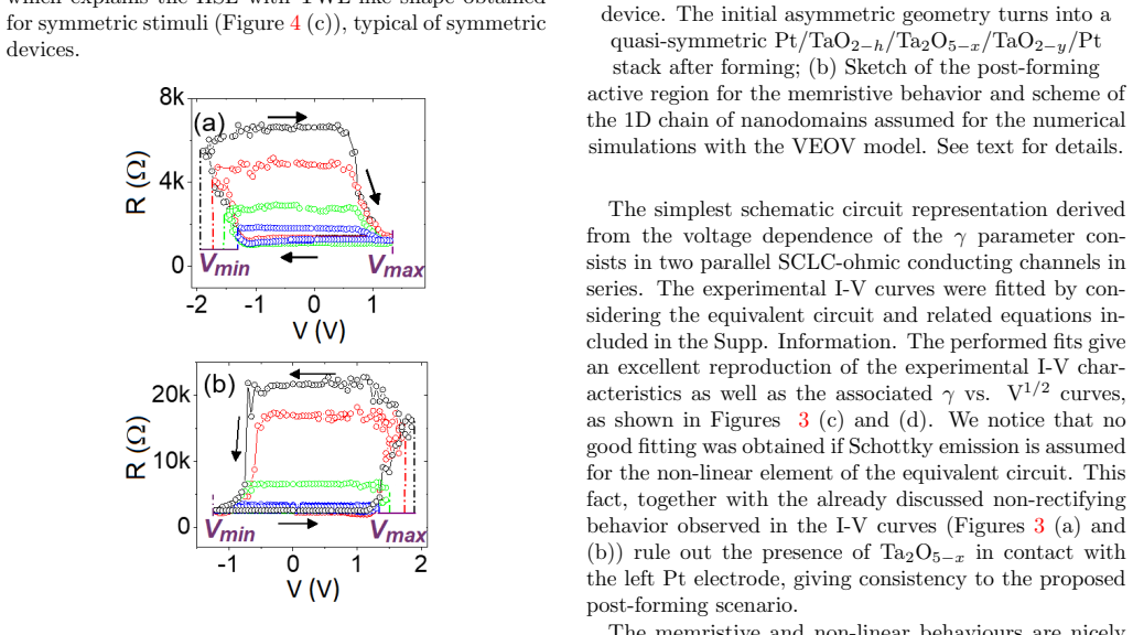
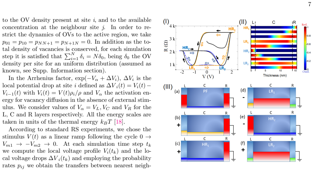
The argument is carried by a three-zone oxygen-vacancy drift model (the VEOV model): the active Ta2O5−x layer is represented as a 1D chain of nanodomains divided into a central bulk zone C and two interfacial zones L and R with lower sensitivity of resistivity to vacancy density. Site resistivity is $\rho_i = \rho_0(1 - A_i\delta_i)$, and vacancy transfer between neighboring sites proceeds with rate probability $p_{ij} = \delta_i(1-\delta_j)\exp(-V_\alpha + \Delta V_i)$, with the total vacancy count conserved. This machinery reproduces, from a single post-forming vacancy profile, the table-with-legs loop for symmetric stimuli and the two squared loops for asymmetric stimuli, and it explains why the active interface is the one whose neighboring electrode drives vacancies into or out of the bulk zone. The two-step rule, one interface drains before the other engages, is the core mechanism.
What would settle it
Take a post-formed device and, while cycling through the asymmetric protocol that gives a squared loop, image the oxygen distribution in cross-section using in-situ TEM/EELS or map local conductance with conductive atomic force microscopy: the claim predicts that only one interface changes its oxygen content and resistance during that cycle, and that the switching side flips when Vmax and Vmin are exchanged. Observing switching at a single fixed location regardless of stimulus asymmetry would refute it.
Extended reading notes
Core claim
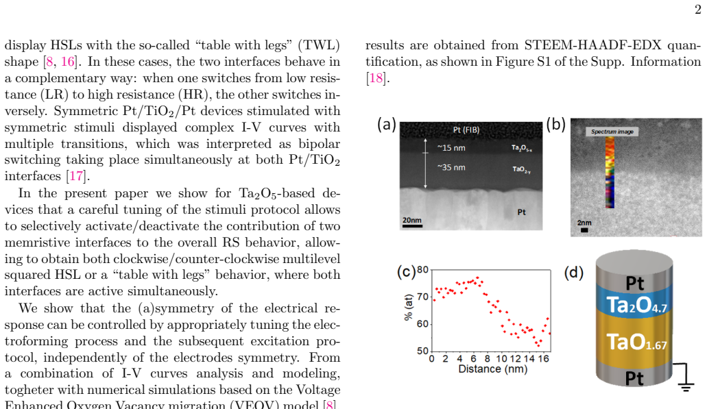
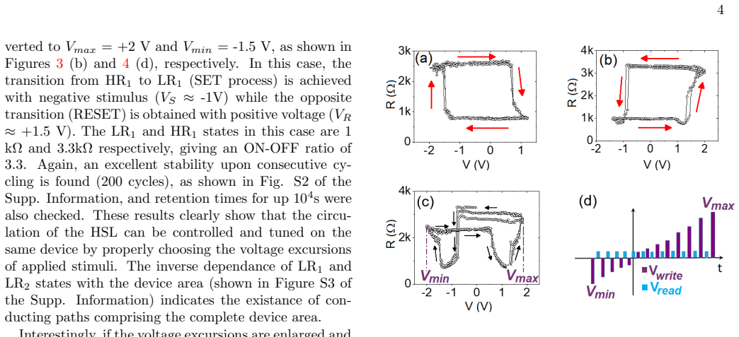
The central claim is that the post-forming structure of these devices is a quasi-symmetric Pt/TaO2−h/Ta2O5−x/TaO2−y/Pt stack in which both oxide/metal-like interfaces are memristive and behave independently depending on stimulus amplitude. By choosing Vmax and Vmin, one interface's oxygen vacancies exchange with the central bulk layer while the other interface remains ohmic, yielding a single active interface and a squared clockwise or counter-clockwise hysteresis switching loop; with symmetric stimuli neither interface is pinned, both exchange vacancies, and the loop acquires the `table with legs' shape. The inversion of loop circulation is not tied to electrode work function, since replacing Pt by Au leaves the behavior unchanged. The paper further claims that the two-step vacancy-transfer process, in which one interface must be almost drained before the other begins to exchange with the bulk, is the physical origin of this selective activation.
Load-bearing premise
The load-bearing premise is that after forming the device really contains a continuous quasi-symmetric stack with two active interfaces in series, as inferred from non-rectifying I-V curves and ex-situ microscopy; if switching is actually localized in one filament or one asymmetric interface, the three-zone vacancy mechanism does not apply.
Editorial extensions
If this is right
- The same device can be programmed to clockwise, counter-clockwise, or table-with-legs loops, so loop direction becomes a controllable degree of freedom rather than a fixed property of electrode asymmetry.
- Multilevel remanent resistance states are available in both loop directions, so synaptic weight can be incremented or decremented with pulses of the same polarity.
- Because only one CMOS-compatible oxide and one metal are needed at room temperature, the functionality is accessible to simple, scalable fabrication.
- Since the behavior is independent of the electrode metal, the effect should transfer to devices with Pt, Au, or other metal top electrodes.
- For memory arrays, the direction of the hysteresis switching loop can be chosen to optimize the ON-OFF ratio for a given application.
Reading between the lines
- If the three-zone volumetric mechanism is generic, other binary oxides with metastable suboxide phases (such as TiO2) may show the same selective-interface control under the right forming protocol, not just TaOx.
- A practical extension suggested by the paper but not tested there: using intermediate voltage amplitudes to write multiple intermediate vacancy profiles could yield a larger number of stable levels than the two-state demonstration, possibly approaching analog conductance tuning for crossbar arrays.
- The forming-polarity dependence implies that the first electrical step can be used to choose which interface is active, a design handle for resistive-switch cells that require a predefined switching direction.
Signed reviews
Editorial analysis
A structured set of objections, weighed in public.
Referee Report
Summary. The manuscript reports that TaOx bilayer devices, initially Pt/Ta2O4.70/TaO1.67/Pt, can be electrically formed into a state that displays memristive hysteresis switching loops (HSLs) whose circulation direction is controlled by the asymmetry of the applied voltage protocol: clockwise for one asymmetric excursion, counter-clockwise for the inverted excursion, and a table-with-legs shape for symmetric excursions. The devices show multilevel remanent resistance states, 200-cycle stability, retention up to 10^4 s, and area-dependent resistance. The authors propose that the post-forming device contains a quasi-symmetric TaO2-h/Ta2O5-x/TaO2-y stack with two memristive interfaces in series, and they interpret the switching as oxygen-vacancy electromigration between a central bulk zone and one or the other interfacial zone, supported by equivalent-circuit fits and VEOV model simulations.
Significance. If the two-interface mechanistic interpretation holds, the work would demonstrate a simple route to tunable switching polarity in a CMOS-compatible oxide, with potential relevance for neuromorphic and non-standard logic devices. The experimental phenomenology is valuable: the CW/CCW/TWL loop control is clearly demonstrated, the 200-cycle stability and retention data support reproducibility, the area scaling in Supp. Fig. S3 argues against a single nanofilament, and the use of a second top electrode (Au) in Supp. Fig. S5 is a useful generality check. The main weakness is that the load-bearing physical mechanism rests on an inferred post-forming microstructure and on simulations whose parameters are fitted to the same devices; the evidence is consistent with the model but does not yet exclude plausible single-interface or filamentary alternatives. These strengths and weaknesses are balanced, so the contribution is significant but the mechanistic claim needs stronger support.
major comments (3)
- [Results (post-forming scenario)] The central mechanistic claim—selective activation of two series memristive interfaces—rests on the inferred post-forming stack Pt/TaO2-h/Ta2O5-x/TaO2-y/Pt, which is not directly observed during switching. Non-rectifying I-V curves and equivalent-circuit fits are consistent with this stack, but the paper itself cites alternative TaOx mechanisms for opposite switching polarity from a single interface or a single filament (Refs. 10-12); area-dependent resistance (Supp. Fig. S3) rules out a single nanofilament but does not establish two discrete active interfaces. The positive-forming control devices in Supp. Fig. S4, which are rectifying and therefore have a single active Ta2O5-x interface, are a natural discriminating experiment: if the same asymmetric voltage protocols produced CW and CCW squared HSLs on those devices, the two-interface interpretation would be in doubt, but this control is not reported.
- [Numerical simulations (VEOV model)] The simulation support for the three-zone mechanism is partly circular. The initial OV density profile δi(t0) is 'chosen to guarantee the post forming high resistance state', and the layer sensitivities Ai, activation energies Vα, and chain sizes N_L, N_C, N_R are tuned to reproduce the measured HSLs; Eq. (1) is an ad hoc linear relation. Consequently, the agreement in Fig. 7 demonstrates internal consistency rather than predictive power, and the statement that the model has 'predictive power' is overstated. The manuscript should either provide an independent determination of these parameters or explicitly frame the simulations as a fit.
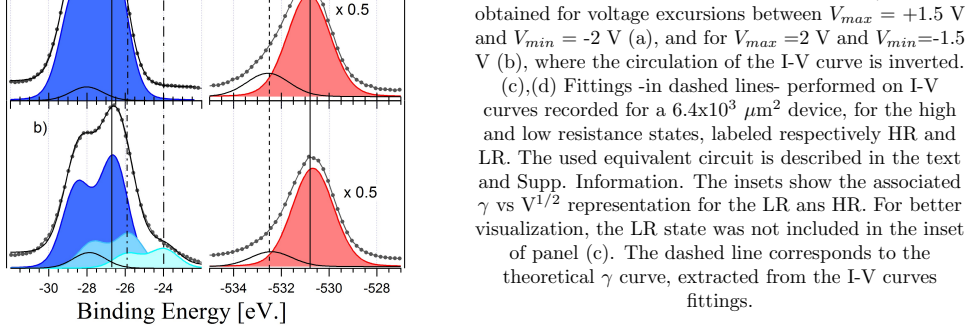
- [Table I and equivalent-circuit assignment] The association of the CCW HSL with the left interface (R1, RNL1) and the CW HSL with the right interface (R2, RNL2) in Table I is inferred from the circuit fits, not from an independent measurement of the interface states. Because the equivalent circuit is a lumped model, the same electrical data could in principle be reproduced by a single interface whose effective barrier or series resistance changes with the voltage protocol; the assignment to two separate interfaces therefore needs additional support, for example switching probed at intermediate states or a control device with one interface passivated.
minor comments (3)
- [Throughout] Several typographical errors should be corrected, including 'scability', 'scketch', 'sinaptic', 'togheter', 'existance', 'characerized', and 'stochiometry'.
- [Figure 1] The caption of Figure 1(c) states that the oxygen concentration quantification comes from data presented in panel (c), but it should refer to panel (b); the text describing the quantification should be checked for consistency.
- [Abstract and Discussion] The claim that the behavior is 'independent of the nature of the used metallic electrodes' is based on Pt and Au top electrodes only, both of which are high-work-function noble metals; this should be stated more cautiously.
Circularity Check
The experimental CW/CCW phenomenon is real, but the VEOV modeling pass is partly circular: the initial OV profile is chosen to reproduce the measured post-forming resistance and the parameters are calibrated to the same HSLs, after which the paper calls the resulting agreement 'predictive power.'
-
fitted input called prediction
[Numerical Simulations, initial OV density profile (Fig. 7, panel III(a))]
"This initial OVs profile is chosen to guarantee the post forming high resistance state, in which the C zone contributes with the dominant resistance, while L and R layers present both a lower resistivity due to a large density of OVs, and contribute little to the total resistance ... This initial profile gives a resistance of 3KΩ, in perfect agreement with the reported experimental value."
The initial OV density profile is an adjustable input of the VEOV model, and the text states it was chosen to guarantee the measured post-forming high-resistance state. Therefore the simulated resistance of 3 kΩ agreeing with the experiment is true by construction, not a prediction. Because this same calibrated profile is the starting point for all simulated HSLs in Fig. 7, the subsequent simulated loop shapes inherit that calibration rather than being an independent first-principles output.
-
fitted input called prediction
[Numerical Simulations, after the simulated TWL-like HSL in Fig. 7(I)]
"The agreement between the simulated and the experimental TWL-like HSL show in Figure 4 (c) is remarkable, denoting the predictive power of the VEOV model."
The paper does not report an out-of-sample prediction. The asymmetric HSL simulations are described as 'emulating the experimental response' after the model parameters and initial OV profile were already adjusted to the measured device. Calling this agreement 'predictive power' renames a calibrated fit as a prediction, since no withheld data or parameter-free forecast is used to validate the model.
full rationale
The headline experimental result—voltage-protocol-controlled CW and CCW squared remanent loops, multilevel states, and TWL behavior—is a genuine measurement and is not itself circular. The circularity is confined to the modeling and interpretation layer. The VEOV simulation starts from an initial OV profile explicitly 'chosen to guarantee the post forming high resistance state,' and the paper then reports the resulting 3 kΩ resistance as being in 'perfect agreement' with the experiment; that is a constructed agreement. The same tuned model is used to reproduce the measured TWL, CW, and CCW HSLs, which the text calls 'emulating the experimental response,' yet the paper also claims 'predictive power of the VEOV model.' That is overclaiming for a calibrated simulation. Additionally, the three-zone L/C/R structure is an assumption imported from the authors' earlier VEOV work (Refs. 8 and 14, with overlapping authorship), and the paper's mechanistic conclusion—oxygen vacancy exchange between a central zone and one of two interfaces—rests on that assumed structure. The equivalent-circuit fits and non-rectifying I-V curves are consistent with two series interfaces, but they do not uniquely force that geometry: a single asymmetric interface or a filamentary mechanism could also produce polarity inversion, and the positive-forming rectifying devices (Supp. Fig. S4) are not used as a discriminating control for the same asymmetric voltage protocols. The experimental phenomenon is independent and valuable, so the paper is not wholly circular, but the model-based 'predictions' partially reduce to fitted inputs, warranting a score of 6.
Assumptions & free parameters
free parameters (4)
- Initial oxygen vacancy density profile δ_i(t0) =
not given; chosen to yield 3 kΩ post-forming resistance
- Layer sensitivity factors A_L, A_R, A_C =
not given in main text (see SI)
- Activation energies V_L, V_C, V_R =
not given in main text (see SI)
- Chain sizes N_L, N_C, N_R =
N_C > N_L = N_R
assumptions (5)
- domain assumption VEOV model equations for OV hopping and local potential drops (from refs [8,14])
- ad hoc to paper Resistivity is a linear decreasing function of local OV density (Eq. 1)
- domain assumption Post-forming stack is quasi-symmetric TaO2-h/Ta2O5-x/TaO2-y with two metallic interfaces
- domain assumption Three-zone structure with distinct L, C, R properties inside the active layer
- standard math Total oxygen vacancy count is conserved during switching
Cite this review
Pith. "Pith review of Electric selective activation of memristive interfaces in TaO$_x$-based devices." pith.science (2026). https://pith.science/paper/5NM62YOL
@misc{pith2026190803056,
  author       = {Pith},
  title        = {Pith review of: Electric selective activation of memristive interfaces in TaO$_x$-based devices},
  year         = {2026},
  howpublished = {\url{https://pith.science/paper/5NM62YOL}},
  note         = {Machine review of arXiv:1908.03056}
}
abstract
The development of novel devices for neuromorphic computing and non-traditional logic operations largely relies on the fabrication of well controlled memristive systems with functionalities beyond standard bipolar behavior and digital ON-OFF states. In the present work we demonstrate for Ta$_2$O$_5$-based devices that it is possible to selectively activate/deactivate two series memristive interfaces in order to obtain clockwise or counter-clockwise multilevel squared remanent resistance loops, just by controlling the (a)symmetry of the applied stimuli and independently of the nature of the used metallic electrodes. Based on our thorough characterization, analysis and modeling, we show that the physical origin of this electrical behavior relies on controlled oxygen vacancies electromigration between three different zones of the active Ta$_2$O$_{5-x}$ layer: a central -- bulk -- one and two quasi-symmetric interfaces with reduced TaO$_{2-h(y)}$ layers. Our devices fabrication process is rather simple as it implies the room temperature deposition of only one CMOS compatible oxide -- Ta-oxide -- and one metal, suggesting that it might be possible to take advantage of these properties at low cost and with easy scability. The tunable opposite remanent resistance loops circulations with multiple -- analogic -- intermediate stable states allows mimicking the adaptable synaptic weight of biological systems and presents potential for non-standard logic devices.
Figures

Figures from the paper (4 more)
Reference graph
Works this paper leans on
-
[1]
(a)symmetric systems give (a)symmetric electrical response
for different resistance states, as labeled respectively in the HSL of panel I); III) Scheme of the L, C and R regions defined in Figure 6 (b), where the colors qualitatively show the different total number of OVs in each region for: (a) post forming (PF) state, (c)-(f) HR1, LR1, HR2 and LR2 states, as labeled in panel I). file along the active region is show...
work page 2017
-
[2]
J. Borghetti, G. S. Snider, P. J. Kuekes, J. J. Yang, D. R. Stewart, and R. S. Williams, Nature 464, 873 (2010)
work page 2010
-
[3]
D. Ielmini and R. Waser, Resistive Switching: From Fun- damentals of Nanoionic Redox Processes to Memristive Device Applications (Wiley-VCH, 2016)
work page 2016
-
[4]
A. Prakash, D. Jana, and S. Maikap, Nanoscale Research Letters 8, 418 (2013)
work page 2013
-
[5]
S. Yu, Neuro-inspiring computing using resistive synaptic devices (Springer International Publishing, 2017)
work page 2017
-
[6]
K. X. Shi, H. Y. Xu, Z. Q. Wang, X. N. Zhao, W. Z. Liu, J. G. Ma, and Y. C. Liu, Applied Physics Letters 111, 223505 (2017), https://doi.org/10.1063/1.5002571
-
[7]
M.-J. Lee, C. B. Lee, D. Lee, S. R. Lee, M. Chang, J. H. Hur, Y.-B. Kim, C.-J. Kim, D. H. Seo, S. Seo, U.-I. Chung, I.-K. Yoo, and K. Kim, Nature Materials 10, 625 (2011)
work page 2011
-
[8]
M. J. Rozenberg, M. J. S´ anchez, R. Weht, C. Acha, F. Gomez-Marlasca, and P. Levy, Phys. Rev. B 81, 115101 (2010)
work page 2010
Show all 33 references
-
[9]
G. H. Baek, A. R. Lee, T. Y. Kim, H. S. Im, and J. P. Hong, Applied Physics Letters 109, 143502 (2016), https://doi.org/10.1063/1.4963884
2016 doi
-
[10]
La Torre, A
C. La Torre, A. Kindsmller, D. J. Wouters, C. E. Graves, G. A. Gibson, J. P. Strachan, R. S. Williams, R. Waser, and S. Menzel, Nanoscale 9, 14414 (2017)
2017
-
[11]
Zhang, Y
H. Zhang, Y. Sijung, S. Menzel, C.-F. W. D. J. H. C. S. W. R. Funck, Carsten, and S. Hoffmann-Eifert, ACS Applied Materials and Interfaces 10, 29766 (2018)
2018
-
[12]
T. H. Park, H. J. Kim, W. Y. Park, S. G. Kim, B. J. Choi, and C. S. Hwang, Nanoscale 9, 6010 (2017)
2017
-
[13]
T. H. Park, S. J. Song, H. J. Kim, S. G. Kim, S. Chung, B. Y. Kim, K. J. Lee, K. M. Kim, B. J. Choi, and C. S. Hwang, Scientific Reports 5, 15965 (2015)
2015
-
[14]
Ghenzi, M
N. Ghenzi, M. J. S´ anchez, and P. Levy, Journal of Physics D: Applied Physics 46, 415101 (2013)
2013
-
[15]
Y. Yang, P. Sheridan, and W. Lu, Applied Physics Let- ters 100, 203112 (2012)
2012
-
[16]
X. Chen, N. J. Wu, J. Strozier, and A. Ig- natiev, Applied Physics Letters 87, 233506 (2005), https://doi.org/10.1063/1.2139843
2005 doi
-
[17]
Ghenzi, M
N. Ghenzi, M. J. S´ anchez, D. Rubi, M. J. Rozenberg, C. Urdaniz, M. Weissman, and P. Levy, Applied Physics Letters 104, 183505 (2014)
2014
-
[18]
for further details on the numerical values of the pa- rameters employed in the simulations. As it was already described in Sec., the negative form- ing sets the device in a high resistance state, associ- ated to which we define an initial OV density profile, δi(t0)∀i = 1..N, to...
-
[19]
D. S. Jeong, H. Schroeder, and R. Waser, Nanotechnol- ogy 20, 375201 (2009)
2009
-
[20]
See Supporting Information for details
-
[21]
Simpson, R
R. Simpson, R. G. White, J. F. Watts, and M. A. Baker, Applied Surface Science 405, 79 (2017)
2017
-
[22]
V. Y.-Q. Zhuo, Y. Jiang, M. H. Li, E. K. Chua, Z. Zhang, J. S. Pan, R. Zhao, L. P. Shi, T. C. Chong, and J. Robert- son, Applied Physics Letters 102, 062106 (2013)
2013
-
[23]
Okamoto, Journal of Phase Equilibria 22, 515 (2001)
H. Okamoto, Journal of Phase Equilibria 22, 515 (2001)
2001
-
[24]
S. P. Garg, N. Krishnamurthy, A. Awasthi, and M. Venkatraman, Journal of Phase Equilibria 17, 63 (1996)
1996
-
[25]
J. J. Yang, M.-X. Zhang, J. P. Strachan, F. Miao, M. D. Pickett, R. D. Kelley, G. Medeiros-Ribeiro, and R. S. Williams, Applied Physics Letters 97, 232102 (2010)
2010
-
[26]
Z. Wei, Y. Kanzawa, K. Arita, Y. Katoh, K. Kawai, S. Muraoka, S. Mitani, S. Fujii, K. Katayama, M. Iijima, T. Mikawa, T. Ninomiya, R. Miyanaga, Y. Kawashima, K. Tsuji, A. Himeno, T. Okada, R. Azuma, K. Shi- makawa, H. Sugaya, T. Takagi, R. Yasuhara, K. Horiba, H. Kumigashira, ...
2008
-
[27]
Y. C. Yang, C. Chen, F. Zeng, and F. Pan, Journal of Applied Physics 107, 093701 (2010)
2010
-
[28]
Acha, Journal of Applied Physics 121 (2017), 10.1063/1.4979723
C. Acha, Journal of Applied Physics 121 (2017), 10.1063/1.4979723
2017 doi
-
[29]
C. Acha, A. Schulman, M. Boudard, K. Daoudi, and T. Tsuchiya, Applied Physics Letters 109 (2016), 10.1063/1.4955204
2016 doi
-
[30]
Acevedo Rom´ an, C
W. Acevedo Rom´ an, C. Acha, M. Sanchez, P. Levy, and D. Rubi, Applied Physics Letters 110 (2017), 10.1063/1.4975157
2017 doi
-
[31]
Acha, Journal of Physics D: Applied Physics 44, 345301 (2011)
C. Acha, Journal of Physics D: Applied Physics 44, 345301 (2011)
2011
-
[32]
Cerchez, H
M. Cerchez, H. Langer, M. El Achhab, T. Heinzel, D. Os- termann, H. Lder, and J. Degenhardt, Applied Physics Letters 103, 033522 (2013)
2013
-
[33]
Blasco, N
J. Blasco, N. Ghenzi, J. Su, P. Levy, and E. Miranda, Microelectronics Reliability 55, 1 (2015)
2015
Reviewed August 14, 2026 · model on record in the stance chip above.
Discussion (0). Continue with ORCID to comment.