REVIEW 4 major objections 4 minor 1 cited by
Elongated Nano Domains and Molecular Intermixing induced Doping in Organic Photovoltaic Active Layers with Electric Field Treatment
T0 review · 4 major / 4 minor · reviewed 2026-08-14 · deepseek-v4-flash
Pith's one-line read Electric-field annealing stretches polymer domains, shrinks band gaps
desk verdict A useful XSTM/S study showing field-assisted annealing elongates P3HT/PCBM domains, but the stronger claim about intermixing-induced band-gap collapse needs more statistical and artifact control before it carries the 'competing factors' narrative. read the letter →
The pith
A machine-rendered reading of the paper's core claim, the machinery that carries it, and where it could break.
The reading
What carries the argument
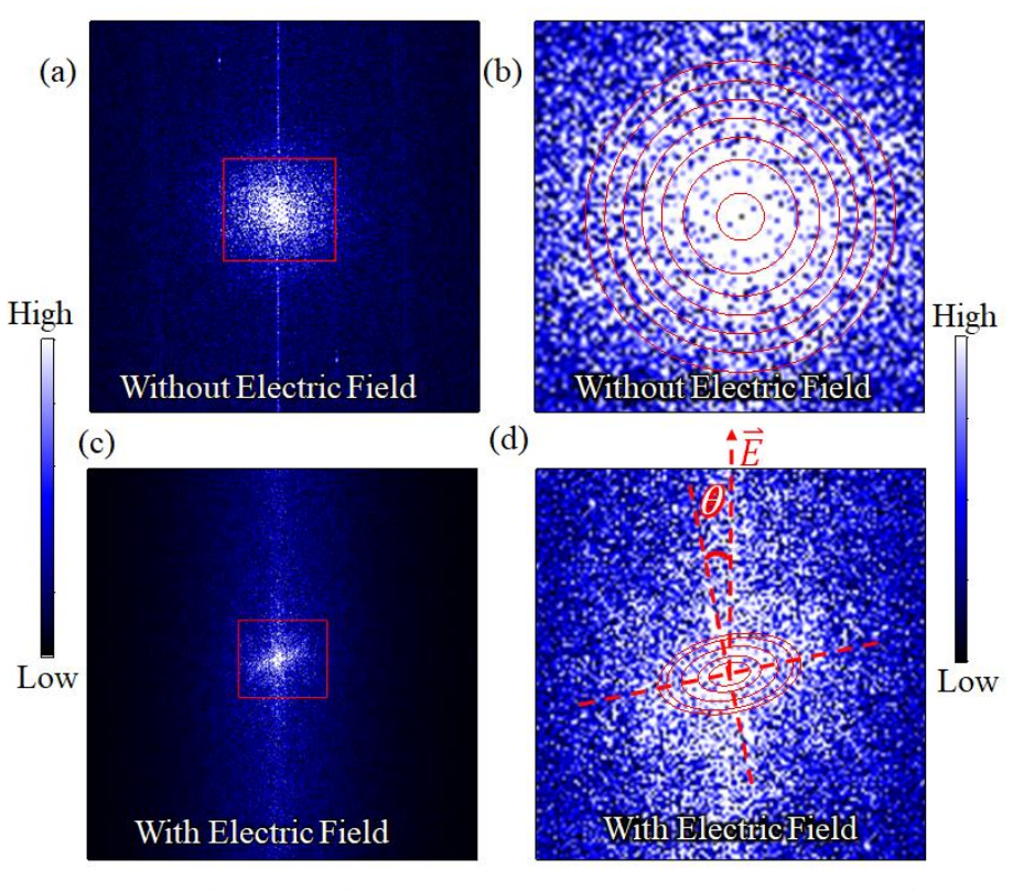
The load-bearing tool is cross-sectional scanning tunneling microscopy and spectroscopy (XSTM/S), in which a freshly fractured film surface is probed with a tip to map topography and dI/dV, a local density-of-states signal that distinguishes P3HT-rich from PCBM-rich domains. The quantitative claim about elongation rests on a 2D Fourier transform of the dI/dV maps: the near-zero-frequency feature is fit by a rotated ellipse Gaussian, and the ellipse's eccentricity and orientation angle give the domain anisotropy and its angle to the electric field. X-ray diffraction and small-angle X-ray scattering supply the supporting claim about intermixing: the downshift of the P3HT (100) peak signals PCBM incorporation into the P3HT lattice, and the narrowed SAXS peak signals a more uniform domain-domain spacing.
What would settle it
Re-measuring band gaps and dI/dV spectra at many independent locations on freshly fractured field-treated and untreated samples, with tip-condition checks and a control surface that has no molecular domains, would settle whether the 0.77/0.59 eV gaps and 0.44 eV offset are intrinsic; if the gap reduction disappears or varies wildly across locations, the intermixing-doping claim fails. Alternatively, if field-treated devices show no drop in open-circuit voltage despite the smaller $\mathrm{LUMO_{acc}}-\mathrm{HOMO_{don}}$ offset, the claimed voltage penalty is not operating.
Extended reading notes
Core claim
On its own terms, the central discovery is that electric-field-assisted annealing of the P3HT/PCBM blend changes both morphology and local electronic structure. In dI/dV maps the treated film shows elongated domains with eccentricity 0.824 ± 0.004 oriented at 6.2° ± 4.8° to the applied field, whereas untreated annealed films are isotropic (eccentricity 0.13 ± 0.06). Point spectra from treated films give band gaps of 0.77 eV for P3HT-rich and 0.59 eV for PCBM-rich regions, compared with 1.62 eV and 1.95 eV without field treatment, and the offset $\mathrm{LUMO_{acc}}-\mathrm{HOMO_{don}}$ drops from 1.57 eV to 0.44 eV. The paper argues that XRD peak shifts show increased P3HT-PCBM intermixing under the field, and that this intermixing dopes the domains and lowers the gaps; the lowered offset would reduce open-circuit voltage while the elongated domains would raise short-circuit current.
Load-bearing premise
The claim rests on assuming that the small set of dI/dV point spectra chosen from high- and low-contrast regions fairly represents the domains, and that the anisotropic band-gap and offset changes are real electronic effects rather than artifacts of the fracture surface or the tip.
Editorial extensions
If this is right
- If field-assisted annealing reliably elongates and aligns donor/acceptor domains, the same treatment should improve charge percolation and short-circuit current in other polar-polymer/fullerene blends.
- If intermixing-induced doping is real, electric fields could be used as a dial to tune domain purity and energy-level alignment, not just crystallinity.
- The competing-effects picture predicts an optimal field strength: enough alignment for current, but not so much intermixing that voltage collapses.
- XRD peak position could become a quick proxy for intermixing level in field-treated active layers.
Reading between the lines
- If the few dI/dV spectra are representative, the field-induced gap reduction is larger than any reported treatment effect, which would make domain-level spectroscopy a sensitive probe of intermixing; this is my inference, not demonstrated here.
- The same mechanism might apply to non-fullerene acceptors with polar donor polymers, since intermixing-induced doping depends on molecular interaction rather than on PCBM specifically; the paper does not test this.
- A direct test would be comparing XSTM/S band gaps with device open-circuit voltage for identical treatment conditions; a linear correlation would strengthen the claimed trade-off.
- Fracture-induced topography remains a confounder: elongated features could partly reflect crack propagation along the field-oriented domains, so measurements on surfaces prepared without fracture would separate morphology from fracture artifact; the paper itself raises this concern.
Signed reviews
Editorial analysis
A structured set of objections, weighed in public.
Referee Report
Summary. This manuscript combines cross-sectional scanning tunneling microscopy/spectroscopy (XSTM/S), X-ray diffraction (XRD), and small-angle X-ray scattering (SAXS) to study how electric-field-assisted annealing affects the nanomorphology and electronic structure of P3HT/PCBM bulk heterojunction active layers. The authors report two main findings: (i) field-assisted annealing produces elongated molecular domains oriented near the electric-field direction (quantified by eccentricity 0.824 ± 0.004 and orientation 6.2° ± 4.8° from six dI/dV maps), and (ii) the same treatment reduces the local band gaps (1.62 eV to 0.77 eV for P3HT-rich and 1.95 eV to 0.59 eV for PCBM-rich regions) and reduces the LUMO(acceptor)-HOMO(donor) offset from 1.57 eV to 0.44 eV, which the authors attribute to PCBM-P3HT intermixing-induced doping. These opposing effects are invoked to explain the moderate performance changes seen in prior device studies.
Significance. If the electronic-structure changes are confirmed, the paper provides a plausible nanoscale explanation for the competing positive and negative effects of electric-field-assisted annealing, namely better percolation (raising Jsc) versus worse energy alignment (lowering Voc). The domain-elongation result is a strength: it is based on quantitative Fourier-transform analysis of six independent dI/dV maps, with explicit fitting (Eq. 1) and reported statistics. The use of XSTM/S on freshly fractured cross-sections is an appropriate method for avoiding annealing artifacts. However, the doping/band-gap conclusion is currently load-bearing and inadequately supported, as it rests on a small number of uncharacterized point spectra without statistical or artifact controls.
major comments (4)
- [Result and Discussion, Fig. 2(f)-(g), pages 8-9] The central claim of intermixing-induced doping rests entirely on dI/dV point spectra taken from 'high and low contrast regions,' with no reported number of spectra, no standard deviations, no setpoint/current conditions, and no tip-condition checks. Because the topographic roughness increases from ~0.2 nm to ~1.2 nm after field treatment, topographic crosstalk or tip-gap changes could suppress the apparent band gaps. The authors should provide statistical distributions of HOMO/LUMO energies across multiple spectra and multiple regions, plus control measurements (e.g., varying setpoint, or spectra on pristine reference samples) to rule out measurement artifacts.
- [Result and Discussion, XRD data, Fig. 4(a) and Table S3, page 11-12] The XRD support for increased intermixing is weak: the (100) peak shifts from 5.30° ± 0.04° (unannealed) to 5.24° ± 0.03° (annealed) to 5.18° ± 0.04° (field-treated), with the last shift comparable to the stated uncertainty, and the peak width is unchanged between annealed and field-treated samples (0.44° ± 0.05° versus 0.42° ± 0.06°). These data do not independently demonstrate that field treatment increases intermixing beyond the annealing effect. The authors should either present higher-precision diffraction data or temper the claim that XRD 'strongly supports' the doping mechanism.
- [Result and Discussion, page 7] The manuscript acknowledges that anisotropic topography 'does not necessarily indicate that the molecular domain textures are anisotropic,' yet the elongation conclusion is drawn from dI/dV maps acquired on the same fracture surfaces. The authors should directly address the possible correlation between fracture-induced topographic features and the apparent dI/dV anisotropy, for example by comparing the orientation and length scale of topographic versus dI/dV features quantitatively, and by showing representative topographic images for all six maps used in the statistics.
- [Result and Discussion, SAXS data, Fig. 4(b) and Table S4, page 13] The SAXS-derived domain-domain distances change from 29.1 nm to 27.6 nm between annealed and field-treated samples, a ~5% difference, while the fitted peak widths change by roughly a factor of two. Given that the dI/dV maps show much more dramatic differences, the SAXS results should be presented with a more explicit discussion of whether these differences are statistically significant and how they connect to the molecular-level intermixing claim, or they should be described as only qualitative.
minor comments (4)
- [Abstract, line 1] There is a typo: 'accepter domains' should be 'acceptor domains.'
- [Conclusion, page 14] The phrase 'in additional to the nanomorphology control' should be 'in addition to the nanomorphology control.'
- [General] For Fig. 2(f)-(g), the authors should state the number of point spectra shown and the acquisition parameters (setpoint current, bias voltage, stabilization time) since these affect the interpretation of dI/dV onsets.
- [Result and Discussion, page 9] The statement that 'the LUMO(acc) - HOMO(don) value changes from 1.57 eV (annealed) to 0.44 eV (electric-field-assisted annealed)' would be clearer if the error bars on these values were reported; currently no uncertainties are given for any of the spectroscopy-derived energy levels.
Circularity Check
No circularity: XSTM/S observations and descriptive fits are self-contained; self-citations are methodological and not load-bearing.
full rationale
I walked the paper's derivation chain: electric-field-assisted annealing -> XSTM topography and dI/dV maps showing elongated domains; STS point spectra giving reduced band gaps and reduced LUMO(acc)-HOMO(don) offset; XRD/SAXS supporting molecular intermixing and doping; and a final competing-effects narrative for Jsc and Voc. None of these steps is a fitted input relabeled as a prediction. The band gaps and orbital offsets are directly measured point-spectrum values, not outputs of a model fit to those same values. The Fourier-analysis ellipse fit (Eq. 1) is a descriptive quantification of eccentricity and orientation from six independent dI/dV maps; it does not create the anisotropy, and the statistics are reported. The XRD and SAXS fits are similarly descriptive. The only self-citations (refs. 35-36, 44-45) support the XSTM/S sample-fracturing methodology; they are applied to new samples and do not presuppose the paper's conclusions. The intermixing-induced-doping interpretation is also supported by an independent literature citation (ref. 34). The paper itself flags a topographic ambiguity ('This anisotropic topography does not necessarily indicate that the molecular domain textures are anisotropic'), but that is a data-interpretation robustness concern, not a circularity. Similarly, the limited STS statistics and the XRD shift comparable to the stated uncertainties weaken evidential strength but do not make the derivation circular. Thus no load-bearing step reduces by construction or by self-citation to its own inputs.
Assumptions & free parameters
assumptions (5)
- domain assumption dI/dV signal is proportional to the local density of states, so HOMO and LUMO positions can be read from the spectra.
- domain assumption The fractured cross-section is representative of the bulk active layer, and fracturing does not alter the nanomorphology or molecular intermixing.
- domain assumption The XRD (100) peak shift to lower angle indicates PCBM incorporation into the P3HT lattice, i.e., intermixing.
- domain assumption The SAXS peak position corresponds to domain-domain distance.
- domain assumption Local LUMO(acc)-HOMO(don) measured by STS determines the device open-circuit voltage.
Cite this review
Pith. "Pith review of Elongated Nano Domains and Molecular Intermixing induced Doping in Organic Photovoltaic Active Layers with Electric Field Treatment." pith.science (2026). https://pith.science/paper/L37NXABH
@misc{pith2026190803229,
  author       = {Pith},
  title        = {Pith review of: Elongated Nano Domains and Molecular Intermixing induced Doping in Organic Photovoltaic Active Layers with Electric Field Treatment},
  year         = {2026},
  howpublished = {\url{https://pith.science/paper/L37NXABH}},
  note         = {Machine review of arXiv:1908.03229}
}
read the original abstract
The effects of the electric-field-assisted annealing on the bulk heterojunction nano-morphology in the P3HT/PCBM active layer of the organic photovoltaic cells (OPVCs) are presented here. It was widely accepted that the electric-field-assisted annealing will facilitate the P3HT, the polar polymer, to be better crystalline to enhance the charge mobility, hence the improvement of the OPVC performance. The influences on the nano-morphology of the electron donor and accepter domains are not well understood. Here, using the cross-sectional scanning tunneling microscopy and spectroscopy (XSTM/S), the electric-field-assisted annealing treatment is found to influence the molecular domains to be elongated with the orientation near the direction of the external electric field. The elongation of the molecular domains is believed to facilitate the domain percolation, which causes higher charge mobility, hence the higher short-circuit current density (Jsc). On the other hand, it was also observed that the electronic properties of the P3HT-rich and PCBM-rich domains in the electric-field-assisted annealed samples showed smaller energy band gaps and smaller molecular orbital offset between the two domains, which is argued to decrease the open circuit voltage (Voc) and negatively impact the OPVC performance. Based on the X-ray diffraction (XRD) and small angle X-ray scattering (SAXS) results, the altered electronic properties are argued to be due to the molecular intermixing induced doping effects. These results point out competing factors affecting the OPVC performance with the electric-field-assisted annealing treatment.
Figures
Forward citations
Cited by 1 Pith paper
-
Designing Anisotropic Microstructures with Spectral Density Function
Adding an anisotropy index to a spectral density function descriptor lets Bayesian optimization discover organic photovoltaic active layers with aligned PCBM wires, raising simulated IPCE from 41.57% to 43.14% versus ...
Reference graph
Works this paper leans on
-
[1]
P. R. Berger and M. Kim, J. Renew. Sustain. Energy 10, 013508 (2018)
work page 2018
- [2]
-
[3]
M. T. Dang, L. Hirsch, and G. Wantz, Adv. Mater. 23, 3597 (2011). 15
work page 2011
- [4]
- [5]
-
[6]
G. Li, V. Shrotriya, J. Huang, Y. Yao, T. Moriarty, K. Emery, and Y. Yang, Nat. Mater. 4, 864 (2005)
work page 2005
-
[7]
Y. A. M. Ismail, T. Soga, and T. Jimbo, Int. J. New Horizons Phys. 93, 87 (2015)
work page 2015
- [8]
Show all 54 references
-
[9]
Kadem, A
B. Kadem, A. Hassan, and W. Cranton, J. Mater. Sci. Mater. Electron. 27, 7038 (2016)
2016
-
[10]
Chambon, L
S. Chambon, L. Derue, M. Lahaye, B. Pavageau, L. Hirsch, and G. Wantz, Materials (Basel). 5, 2521 (2012)
2012
-
[11]
Padinger, R
F. Padinger, R. S. Rittberger, N. S. Sariciftci, F. Padinger, R. S. Rittberger, R. S. Rittberger, N. S. Sariciftci, and N. S. Sariciftci, Adv. Funct. Mater. 13, 85 (2003)
2003
-
[12]
Chang, Y
S. Chang, Y. Hsiao, and T. Li, Int. J. Electrochem. Sci. 10, 1658 (2015)
2015
-
[13]
H. Yu, Y. Li, Y. Dong, and X. Huang, Int. J. Photoenergy 2016, 1 (2016)
2016
-
[14]
G. Li, V. Shrotriya, Y. Yao, and Y. Yang, J. Appl. Phys. 98, 043704 (2005)
2005
-
[15]
Bagui and S
A. Bagui and S. S. K. Iyer, IEEE Trans. Electron Devices 58, 4061 (2011)
2011
-
[16]
Y. M. Shen, C. S. Chen, P. C. Yang, S. Y. Ma, and C. F. Lin, Sol. Energy Mater. Sol. Cells 99, 263 (2012)
2012
-
[17]
Reyes-Reyes, K
M. Reyes-Reyes, K. Kim, and D. L. Carroll, Appl. Phys. Lett. 87, (2005)
2005
-
[18]
C. X. Zhao, X. Wang, W. Zeng, Z. K. Chen, B. S. Ong, K. Wang, L. Deng, and G. Xu, Appl. Phys. Lett. 99, 1 (2011). 16
2011
-
[19]
C. C. Lin, Y. Y. Lin, S. S. Li, C. C. Yu, C. L. Huang, S. H. Lee, C. H. Du, J. J. Lee, H. L. Chen, and C. W. Chen, Energy Environ. Sci. 4, 2134 (2011)
2011
-
[20]
Solanki, B
A. Solanki, B. Wu, T. Salim, E. K. L. Yeow, Y. M. Lam, and T. C. Sum, J. Phys. Chem. C 118, 11285 (2014)
2014
-
[21]
Solanki, A
A. Solanki, A. Bagui, G. Long, B. Wu, T. Salim, Y. Chen, Y. M. Lam, and T. C. Sum, ACS Appl. Mater. Interfaces 8, 32282 (2016)
2016
-
[22]
Vijayan, K
R. Vijayan, K. Swathi, and K. S. Narayan, ACS Appl. Mater. Interfaces 9, 19436 (2017)
2017
-
[23]
Q. Shi, Y. Hou, J. Lu, H. Jin, Y. Li, Y. Li, X. Sun, and J. Liu, Chem. Phys. Lett. 425, 353 (2006)
2006
-
[24]
Zhi-Hui, H
F. Zhi-Hui, H. Yan-Bing, S. Quan-Min, Q. Li-Fang, L. Yan, Z. Lei, L. Xiao-Jun, T. Feng, W. Yong-Sheng, and X. Rui-Dong, Chinese Phys. B 19, 038601 (2010)
2010
-
[25]
H. Jin, Y. Hou, Q. Shi, X. Meng, and F. Teng, Solid State Commun. 140, 555 (2006)
2006
-
[26]
A. K. Pandey, J. M. Nunzi, H. Wang, C. C. Oey, A. B. Djurišić, M. H. Xie, Y. H. Leung, K. K. Y. Man, and W. K. Chan, Org. Electron. 8, 396 (2007)
2007
-
[27]
Y. Li, Y. Hou, Y. Wang, Z. Feng, B. Feng, L. Qin, and F. Teng, Synth. Met. 158, 190 (2008)
2008
-
[28]
T. J. Savenije, J. E. Kroeze, X. Yang, and J. Loos, Thin Solid Films 511–512, 2 (2006)
2006
-
[29]
Vanlaeke, G
P. Vanlaeke, G. Vanhoyland, T. Aernouts, D. Cheyns, C. Deibel, J. Manca, P. Heremans, and J. Poortmans, Thin Solid Films 511–512, 358 (2006)
2006
-
[30]
J. J. Dittmer, E. A. Marseglia, and R. G. Friend, Adv. Mater. 12, 1270 (2000)
2000
-
[31]
T. W. Lee and O. O. Park, Appl. Phys. Lett. 77, 3334 (2000)
2000
-
[32]
T. L. Lim, C. W. Chang, A. R. Inigo, Y. F. Huang, J. D. White, and W. Fann, Chem. Phys. Lett. 432, 564 (2006). 17
2006
-
[33]
M. C. Shih, B. C. Huang, C. C. Lin, S. S. Li, H. A. Chen, Y. P. Chiu, and C. W. Chen, Nano Lett. 13, 2387 (2013)
2013
-
[34]
L. E. Garner, A. Bera, B. W. Larson, D. P. Ostrowski, A. J. Pal, and W. A. Braunecker, ACS Energy Lett. 2, 1556 (2017)
2017
-
[35]
U. F. Ghumman, A. Iyer, R. Dulal, J. Munshi, A. Wang, T. Chien, G. Balasubramanian, and W. Chen, ASME IDETC/CIE 2018 2B, 1 (2018)
2018
-
[36]
U. F. Ghumman, A. Iyer, R. Dulal, J. Munshi, A. Wang, T. Chien, G. Balasubramanian, and W. Chen, J. Mech. Des. 140, 111408 (2018)
2018
-
[37]
W. Wang, S. Guo, E. M. Herzig, K. Sarkar, M. Schindler, D. Magerl, M. Philipp, J. Perlich, and P. Müller-Buschbaum, J. Mater. Chem. A 4, 3743 (2016)
2016
-
[38]
A. L. Ayzner, C. J. Tassone, S. H. Tolbert, and B. J. Schwartz, J. Phys. Chem. 113, 20050 (2009)
2009
-
[39]
B. Y. Kadem, R. G. Kadhim, and H. Banimuslem, J. Mater. Sci. Mater. Electron. 29, 9418 (2018)
2018
-
[40]
M. A. Brady, G. M. Su, and M. L. Chabinyc, Soft Matter 7, 11065 (2011)
2011
-
[41]
Y. M. Chang and L. Wang, J. Phys. Chem. C 112, 17716 (2008)
2008
-
[42]
Vanlaeke, A
P. Vanlaeke, A. Swinnen, I. Haeldermans, G. Vanhoyland, T. Aernouts, D. Cheyns, C. Deibel, J. D’Haen, P. Heremans, J. Poortmans, and J. V. Manca, Sol. Energy Mater. Sol. Cells 90, 2150 (2006)
2006
-
[43]
J. W. Kiel, B. J. Kirby, C. F. Majkrzak, B. B. Maranville, and M. E. Mackay, Soft Matter 6, 641 (2010)
2010
-
[44]
Wang and T
A. Wang and T. Chien, Phys. Lett. A 382, 739 (2018)
2018
-
[45]
A. J. Yost, A. Pimachev, C. C. Ho, S. B. Darling, L. Wang, W. F. Su, Y. Dahnovsky, and 18 T. Chien, ACS Appl. Mater. Interfaces 8, 29110 (2016)
2016
-
[46]
J. Li, M. Xue, N. Xue, H. Li, L. Zhang, Z. Ren, S. Yan, and X. Sun, Langmuir 35, 7841 (2019)
2019
-
[47]
D. E. Motaung, G. F. Malgas, C. J. Arendse, and T. Malwela, Mater. Chem. Phys. 124, 208 (2010)
2010
-
[48]
H. Li, Z. Chen, H. Tang, W. Xu, J. Li, X. Zhao, and X. Yang, RSC Adv. 2, 10231 (2012)
2012
-
[49]
Seidler, G
N. Seidler, G. M. Lazzerini, G. Li Destri, G. Marletta, and F. Cacialli, J. Mater. Chem. C 1, 7748 (2013)
2013
-
[50]
W. Wang, C. Chen, C. Tollan, F. Yang, Y. Qin, and M. Knez, J. Mater. Chem. C 5, 2686 (2017)
2017
-
[51]
F. Liu, D. Chen, C. Wang, K. Luo, W. Gu, A. L. Briseno, J. W. P. Hsu, and T. P. Russell, ACS Appl. Mater. Interfaces 6, 19876 (2014)
2014
-
[52]
A. J. Parnell, A. J. Cadby, O. O. Mykhaylyk, A. D. F. Dunbar, P. E. Hopkinson, A. M. Donald, and R. A. L. Jones, Macromolecules 44, 6503 (2011)
2011
-
[53]
Ophir and G
Z. Ophir and G. L. Wilkes, J. Polym. Sci. Polym. Phys. Ed. 18, 1469 (1980)
1980
-
[54]
Huang, C.-S
Y.-C. Huang, C.-S. Tsao, C.-M. Chuang, C.-H. Lee, F.-H. Hsu, H.-C. Cha, C.-Y. Chen, T.-H. Lin, C.-J. Su, U.-S. Jeng, and W.-F. Su, J. Phys. Chem. C 116, 10238 (2012)
2012
Reviewed August 14, 2026 · model on record in the stance chip above.
Discussion (0). Continue with ORCID to comment.