REVIEW 3 major objections 4 minor 64 references
Electronic properties of air-exposed GaN$(1\bar{1}00)$ and $(0001)$ surfaces after several device processing compatible cleaning steps
T0 review · 3 major / 4 minor · reviewed 2026-08-14 · deepseek-v4-flash
Pith's one-line read Under ultraviolet illumination, the work function of HCl-cleaned GaN surfaces drops by at least 0.2 eV while the Ga 2p3/2 core level does not move, showing the photovoltage is a light-induced surface-dipole change, not band-bending…
desk verdict New quantitative GaN(1-100) band-bending and work-function data after common cleanings, with a UV-induced dipole effect on HCl surfaces that is supported by sub-band-gap KPFM. read the letter →
The pith
A machine-rendered reading of the paper's core claim, the machinery that carries it, and where it could break.
The reading
What carries the argument
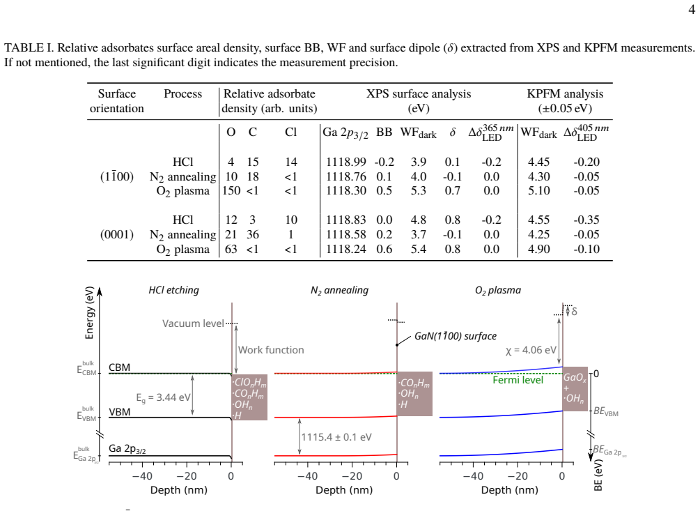
The analysis rests on two complementary probes and a bookkeeping identity. Band bending is extracted from the Ga $2p_{3/2}$ core-level binding energy through $$\mathrm{BB} = [E_{\mathrm{VBM}} - E_{\mathrm{Ga}\,2p_{3/2}}] + E_g - BE_{\mathrm{Ga}\,2p_{3/2}} - [E_{\mathrm{CBM}} - E_F]_{\mathrm{bulk}},$$ using the measured constant $[E_{\mathrm{VBM}} - E_{\mathrm{Ga}\,2p_{3/2}}] = 1115.4\pm0.1$ eV; the work function is read from the secondary-electron cutoff, and the Kelvin probe gives the contact potential difference. Subtracting the band bending from the work function, with the electron affinity taken as 4.06 eV, isolates the surface dipole $\delta$. The decisive move is the illumination comparison: when the core levels do not shift under UV light, any measured work-function change must equal a change in the surface dipole, $\Delta\delta_{\mathrm{LED}} = WF_{\mathrm{LED}} - WF_{\mathrm{dark}}$. The three cleaning steps are themselves part of the machinery, since they serve as the controllable way to populate or strip specific adsorbate terminations ($\cdot\mathrm{ClO}_n\mathrm{H}_m$, $\cdot\mathrm{CO}_n\mathrm{H}_m$, $\cdot\mathrm{OH}_n$, $\cdot\mathrm{H}$, and $\mathrm{GaO}_x + \cdot\mathrm{OH}_n$).
What would settle it
Measure the Ga $2p_{3/2}$ core-level position under the same 365 nm illumination with a detection limit below roughly 50 meV (for example, by longer acquisition or a calibrated reference line). If any core-level shift appears on the HCl-treated surfaces while the work function drops by 0.2 eV, part of the photovoltage is band-bending screening, and the dipole-only attribution would be falsified.
Extended reading notes
Core claim
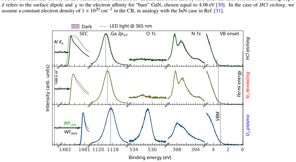
On n-type GaN(1-100) and GaN(0001) surfaces exposed to air, the three cleaning steps reproducibly produce very different electronic landscapes. HCl etching leaves Cl- and H-containing adsorbates that act as surface donors, giving flat bands on (0001) and downward band bending with an electron accumulation layer on (1-100). Annealing at 400–500 °C in N2 removes the Cl and yields a moderate 0.1–0.2 eV upward band bending, while O2 plasma forms a thin GaOx capping layer with OH terminations and drives a 0.5–0.6 eV upward band bending together with a large inward surface dipole. Under 365 nm illumination, no Ga $2p_{3/2}$ core-level shift is observed on any surface, ruling out photo-induced screening of the band bending. Yet on the HCl-treated surfaces the work function drops by at least 0.2 eV, so the authors attribute the surface photovoltage to a photo-induced change of the surface dipole built by the Cl/OH adsorbates. The conclusion is that Kelvin-probe surface photovoltage alone cannot separate dipole changes from band-bending screening, so earlier interpretations of such measurements on HCl-treated GaN need revision.
Load-bearing premise
The claim that the 0.2 eV UV-induced work-function drop is entirely a surface-dipole effect rests on the assumption that the XPS core-level measurement would have detected any band-bending screening of a few tens of millielectronvolts, since the paper reports no core-level shift without stating the detection limit.
Editorial extensions
If this is right
- Kelvin-probe surface photovoltage measurements on HCl-treated GaN cannot be read directly as band-bending screening; a UV-induced work-function drop of at least 0.2 eV can be a pure surface-dipole effect.
- The three cleaning steps give a practical recipe to set air-exposed GaN(1-100) and GaN(0001) surfaces into defined electronic states, with band bending tunable over several hundred millielectronvolts and the work function by more than 1 eV in vacuum.
- HCl etching produces an electron accumulation layer on GaN(1-100), so Cl/H adsorbates act as surface donors rather than merely removing surface states.
- O2 plasma exposure, by creating a thin GaOx layer with OH terminations, drives a large upward band bending and inward dipole, a state that must be accounted for when later processing contacts on the surface.
- Earlier reports that interpret UV-induced photovoltage on HCl-treated GaN only in terms of band-bending screening (references [3,7,59-61]) should be revisited with a core-level probe.
Reading between the lines
- If the 0.2 eV photo-induced dipole drop is specific to Cl/H termination, dosing a clean GaN surface with HCl in vacuum and cycling the UV light should reproduce the effect; if it appears only after air exposure, co-adsorbed water or oxygen is part of the mechanism.
- The result implies contact-barrier engineering on GaN may be achievable purely through surface chemistry: because the cleaning steps change the work function by more than the band bending, Schottky barrier heights on air-exposed GaN should shift by roughly the dipole change, a prediction the paper does not test.
- The same two-channel picture (band-bending screening plus dipole change) likely applies to other III-nitrides and to oxide-covered semiconductors; comparative Kelvin-probe/XPS measurements under sub-band-gap versus above-band-gap illumination would show whether the dipole channel is a general adsorbate phenomenon.
- Because the paper relies on a single electron-affinity value (4.06 eV) for absolute dipole amplitudes, a direct measurement of the affinity on atomically clean surfaces of both orientations would sharpen all quantitative dipole estimates; the relative trends between cleaning steps would presumably survive.
Signed reviews
Editorial analysis
A structured set of objections, weighed in public.
Referee Report
Summary. The manuscript reports a combined XPS and Kelvin-probe study of the electronic properties of air-exposed GaN(1-100) and GaN(0001) surfaces subjected to three device-processing-compatible cleaning steps: HCl etching, annealing in N2, and O2 plasma exposure. The authors quantify adsorbate coverages, band bending, work function, and surface dipoles in the dark and under UV illumination. The central claim is that on HCl-treated surfaces, UV illumination reduces the work function by at least 0.2 eV while the XPS core levels do not shift, implying that the band bending is not screened and that the work-function change is a photo-induced modification of the surface dipole. On this basis the authors argue that surface photovoltage measurements by Kelvin probe alone cannot be used to characterize GaN surface band bending.
Significance. If the central claim holds, the paper provides practically useful cleaning protocols for resetting air-exposed GaN surfaces into defined electronic states and delivers a cautionary result for the interpretation of Kelvin-probe surface photovoltage measurements on GaN. The strength of the paper is that the relative trends across cleaning steps are directly measured with two complementary techniques, the work-function span is large and internally consistent, and the adsorbate analysis supports the qualitative picture of cleaning-dependent surface dipoles. However, the load-bearing conclusion that the observed photovoltage is entirely a surface-dipole effect rests on an unquantified null result: the reported absence of core-level shifts is given without a detection limit. The absolute band-bending values also depend on a self-calibrated reference, which adds systematic uncertainty to the absolute claims. These issues are addressable but require revision.
major comments (3)
- [Section III.D and Table I] The central claim that the work-function decrease of HCl-treated surfaces under 365 nm illumination occurs 'without screening of the band bending' is supported only by the statement that 'no shift of the core levels' is observed. No detection limit, confidence interval, or repeated-measurement statistics are reported for the Ga 2p3/2 or N 1s centroid positions in the dark/illuminated comparison. The Au Fermi-edge control described in Section II checks for charging, not for the minimum band-bending change that would be visible in the GaN core levels. On the GaN(0001) HCl surface, whose reported dark band bending is 0.0 eV, a surface photovoltage of 0.1-0.2 eV would lower the work function by exactly the observed amount and would be masked by an unquantified 'no shift.' Please provide the centroid shift, its uncertainty, and an explicit statement of the minimum detectable surface photovoltage, or restrict the conclusion accordingly.
- [Section III.B, Eq. (1)] The absolute band-bending scale is set by the material constant [E_VBM - E_Ga2p3/2] = 1115.4 +/- 0.1 eV, which the authors obtain by averaging their own 25 XPS spectra of GaN samples with different orientations and adsorbates. If those spectra were not acquired at flat band, the zero of the absolute band-bending scale is systematically offset, and the stated uncertainty of 0.1 eV reflects only the uncertainty in the VBM linear fit, not this systematic effect. This matters for the absolute claims of 'flat band' after HCl etching on GaN(0001) and a downward band bending of -0.2 eV on GaN(1-100), as well as for the derived surface-dipole amplitudes. Please provide a calibration of the bulk reference against an independently known flat-band condition, or explicitly state the systematic uncertainty and temper the absolute values.
- [Section III.D and Section II] The XPS and KPFM illumination conditions are not equivalent: the XPS measurements use a 365 nm LED with an excitation density of 10-100 mW/cm2, whereas the KPFM measurements use a 405 nm LED with an excitation density of about 0.1 mW/cm2. The no-screening evidence comes exclusively from the XPS measurements at 365 nm, while the KPFM data at 405 nm are presented as complementary values of the same surface-dipole change. Since the magnitude of a surface photovoltage depends strongly on photon energy and excitation density, the two data sets are not directly comparable. Please either perform the KPFM measurements under the same above-band-gap illumination conditions, or explicitly restrict the claim to the 365 nm excitation used for the XPS core-level null result.
minor comments (4)
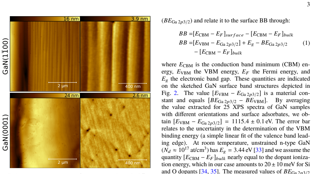
- [Section III.C and Table I] The text states that the work function is modulated over a range of 0.6 eV in N2 atmosphere, but the KPFM values in Table I span from 4.25 to 5.10 eV, i.e., about 0.85 eV. Please clarify whether the 0.6 eV value refers to a single orientation or correct the statement.
- [Section III.C] The electron affinity of 4.06 eV used for the dipole estimates is taken from a scanning tunneling spectroscopy study of the GaN(1-100) surface and is applied to the GaN(0001) surface as well. Please justify this transfer or add a caveat that the absolute dipole values for GaN(0001) are approximate.
- [Section III.D and Fig. 3] The statement that 'similar trends are observed for the cleaned GaN(0001) surface' would be better supported by showing the corresponding dark/illumination core-level spectra for the GaN(0001) surface, particularly for the O2-plasma-treated case where a large upward band bending is claimed.
- [Section II] The comparison between XPS (vacuum, 365 nm) and KPFM (N2 atmosphere, 405 nm) results would benefit from an explicit discussion of how the different measurement environments and photon energies affect the observed work-function changes, especially the role of physisorbed water.
Circularity Check
No significant circularity: the band-bending extraction is a standard core-level calibration and the UV-dipole attribution rests on direct measurements, not on its own inputs.
full rationale
The paper's central derivation chain does not reduce to its inputs. Equation (1) converts Ga 2p3/2 binding energies into band bending using the core-level-to-VBM offset [EVBM - EGa2p3/2] = 1115.4 +/- 0.1 eV, which the authors obtain by averaging 25 of their own XPS spectra. This is a material-constant calibration, not a fitted parameter that predetermines the reported band-bending values: band bending shifts the VBM and the Ga 2p3/2 level rigidly together, so their difference is independent of the actual band bending of the calibration spectra. The bulk Fermi-level term [ECBM - EF]bulk = 20 +/- 10 meV is taken from external references [34,35], not from the same fit, so the absolute BB scale is not self-referential. The UV illumination conclusion in Section III.D rests on the directly observed constancy of the core-level positions under illumination and the measured work-function decrease; attributing the work-function decrease to a surface-dipole change is a conditional inference from the asserted absence of band-bending screening. The 'no shift of the core levels' claim is an unquantified null result without a stated detection limit, which is a legitimate experimental-evidence concern but not a circularity. The paper contains no load-bearing self-citations and invokes no uniqueness result from its own authors to forbid alternatives. The derivation is therefore self-contained against external measurements and calibration references, and no circular step can be exhibited.
Assumptions & free parameters
free parameters (2)
- Bulk reference [E_VBM - E_Ga2p3/2] =
1115.4 ± 0.1 eV
- Assumed electron density in conduction band for HCl-etched GaN(1-100) =
1 x 10^20 cm^-3
assumptions (5)
- domain assumption The Ga 2p3/2 binding energy shift relative to the valence band maximum is a material constant independent of surface preparation.
- domain assumption The absence of core-level shifts under UV illumination implies no band-bending screening.
- domain assumption The thin GaOx layer formed by O2 plasma can be treated as a single GaN/ambient interface rather than a two-interface heterostructure.
- domain assumption KPFM work-function values calibrated against HOPG (4.5 eV) are accurate to the stated precision.
- domain assumption The electron affinity chi = 4.06 eV for bare GaN(1-100) from Ref [30] is accurate enough to estimate absolute surface dipoles.
Cite this review
Pith. "Pith review of Electronic properties of air-exposed GaN$(1\bar{1}00)$ and $(0001)$ surfaces after several device processing compatible cleaning steps." pith.science (2026). https://pith.science/paper/3MGIAD6V
@misc{pith2026190803376,
  author       = {Pith},
  title        = {Pith review of: Electronic properties of air-exposed GaN$(1\bar100)$ and $(0001)$ surfaces after several device processing compatible cleaning steps},
  year         = {2026},
  howpublished = {\url{https://pith.science/paper/3MGIAD6V}},
  note         = {Machine review of arXiv:1908.03376}
}
abstract
We report on the electronic properties of GaN$(1\bar{1}00)$ and $(0001)$ surfaces after three different and subsequent device processing compatible cleaning steps: HCl etching, annealing at $400$ $^\circ$C in N$_2$ atmosphere, and O$_2$ plasma exposure. The surface electronic properties are quantified, in the dark and under ultraviolet illumination, using X-ray photoelectron spectroscopy and a Kelvin probe. We find that the cleaning steps largely affect the work function and the band bending of both GaN orientations. These modifications are attributed to the presence of different surface states as well as to the formation of adsorbates building up distinct surface dipoles. Besides these results, we detect that under ultraviolet illumination the work function of the surfaces exposed to HCl decreases by at least $0.2$ eV without screening of the band bending. We thus attribute the observed surface photovoltage to a photo-induced modification of the surface dipole. Overall, these results emphasize the strong dependence of the electronic properties of air-exposed GaN surfaces on adsorbates. As a result, we advocate the use of the common cleaning steps analyzed here to re-initialize at will GaN$(1\bar{1}00)$ and $(0001)$ surfaces into pre-defined states.
Figures
Reference graph
Works this paper leans on
-
[1]
HCl etching: the GaN sample is dipped for10min in a 32% HCl (< 0.0012% contaminants) aqueous solutionandsubsequentlyrinsedinaboiling 99%pure ethylacetate solvent
-
[2]
Annealing: theGaNsampleisannealedat 400–500◦C for a minimum of20min in a N2 atmosphere
-
[3]
O2 plasma: the GaN sample is exposed for5min to an O2 plasma (forward power of900W in a O2 atmo- sphere of 0.3mbar), which is conceptually similar to UV/O3 exposure, although a larger kinetic energy is provided to O radicals. As largely reported for the GaN(0001) surface, HCl etch- ingdecreases to low levels the areal concentration of typical surface cont...
work page 2016
- [4]
-
[5]
P.-S.Chen,T.-H.Lee,L.-W.Lai, andC.-T.Lee,J.Appl.Phys. 101, 024507 (2007)
work page 2007
-
[6]
I. Shalish, Y. Shapira, L. Burstein, and J. Salzman, J. Appl. Phys. 89, 390 (2001)
work page 2001
-
[7]
S. Tripathy, S. J. Chua, and A. Ramam, J. Phys. Condens. Matter 14, 4461 (2002)
work page 2002
-
[8]
M.Foussekis,A.A.Baski, andM.A.Reshchikov,Appl.Phys. Lett. 94, 16 (2009)
work page 2009
Show all 64 references
-
[9]
Pfüller, O
C. Pfüller, O. Brandt, F. Grosse, T. Flissikowski, C. Chèze, V. Consonni, L. Geelhaar, H. T. Grahn, and H. Riechert, Phys. Rev. B82, 045320 (2010)
2010
-
[10]
R.GurwitzandI.Shalish,Nanotechnology 22,435705(2011)
2011
-
[11]
N. A. Sanford, L. H. Robins, P. T. Blanchard, K. Soria, B. Klein, B. S. Eller, K. A. Bertness, J. B. Schlager, and A. W. Sanders, J. Appl. Phys.113, 174306 (2013)
2013
-
[12]
González-Posada, R
F. González-Posada, R. Songmuang, M. Den Hertog, and E. Monroy, Appl. Phys. Lett.102, 21 (2013)
2013
-
[13]
J.-H. Kim, D. Elmaghraoui, M. Leroux, M. Korytov, P. Ven- néguès, S. Jaziri, J. Brault, and Y.-H. Cho, Nanotechnology 25, 305703 (2014)
2014
-
[14]
Ramírez-López, J
Łukasz Janicki, M. Ramírez-López, J. Misiewicz, G. Cy- wiński, M. Boćkowski, G. Muzioł, C. Chèze, M. Sawicka, C. Skierbiszewski, and R. Kudrawiec, Jpn. J. Appl. Phys.55, 05FA08 (2016)
2016
-
[15]
147, 104703 (2017)
Q.Wang,A.Puntambekar, andV.Chakrapani,J.Chem.Phys. 147, 104703 (2017)
2017
-
[16]
JiříŁek, J
I.Bartoš,O.Romanyuk,J.Houdkova,P.P.Paskov,T.Paskova, and P. JiříŁek, J. Appl. Phys.119, 10 (2016)
2016
-
[17]
U. Behn, A. Thamm, O. Brandt, and H. T. Grahn, J. Appl. Phys. 87, 4315 (2000)
2000
-
[18]
M.Hetzl,M.Kraut,T.Hoffmann,J.Winnerl,K.Boos,A.Zei- dler, I. D. Sharp, and M. Stutzmann, J. Appl. Phys. 124, 035704 (2018)
2018
-
[19]
Y. Dong, R. M. Feenstra, and J. E. Northrup, J. Vac. Sci. Technol. B24, 2080 (2006)
2006
-
[20]
89, 17 (2006)
Y.Dong,R.M.Feenstra, andJ.E.Northrup,Appl.Phys.Lett. 89, 17 (2006)
2006
-
[21]
Bermudez, Surf
V. Bermudez, Surf. Sci. Rep.72, 147 (2017)
2017
-
[22]
J. Shao, L. Tang, C. Edmunds, G. Gardner, O. Malis, and M. Manfra, J. Appl. Phys.114, 023508 (2013)
2013
-
[23]
C. B. Lim, A. Ajay, and E. Monroy, Appl. Phys. Lett.111, 022101 (2017)
2017
-
[24]
Uhlrich, L
J. Uhlrich, L. Grabow, M. Mavrikakis, and T. Kuech, J. Elec- tron. Mater.37, 439 (2008)
2008
-
[25]
K. A. Rickert, A. B. Ellis, F. J. Himpsel, J. Sun, and T. F. Kuech, Appl. Phys. Lett.80, 204 (2002)
2002
-
[26]
Irokawa, T
Y. Irokawa, T. T. Suzuki, K. Yuge, A. Ohi, T. Nabatame, K. Kimoto, T. Ohnishi, K. Mitsuishi, and Y. Koide, Jpn. J. Appl. Phys.56, 128004 (2017)
2017
-
[27]
Irokawa, K
Y. Irokawa, K. Mitsuishi, T. T. Suzuki, K. Yuge, A. Ohi, T. Nabatame, T. Ohnishi, K. Kimoto, and Y. Koide, Jpn. J. Appl. Phys.57, 098003 (2018)
2018
-
[28]
D. A. Shirley, Phys. Rev. B5, 4709 (1972)
1972
-
[29]
J. P. Long and V. M. Bermudez, Phys. Rev. B66, 121308 (2002)
2002
-
[30]
J.Colchero,A.Gil, andA.M.Baró,Phys.Rev.B 64,245403 (2001)
2001
-
[31]
W. N. Hansen and G. J. Hansen, Surf. Sci.481, 172 (2001)
2001
-
[32]
Scofield, J
J. Scofield, J. Electron Spectros. Relat. Phenomena8, 129 (1976)
1976
-
[33]
Portz, M
V. Portz, M. Schnedler, H. Eisele, R. E. Dunin-Borkowski, and P. Ebert, Phys. Rev. B97, 115433 (2018). 7
2018
-
[34]
Mahboob, T
I. Mahboob, T. D. Veal, C. F. McConville, H. Lu, and W. J. Schaff, Phys. Rev. Lett.92, 036804 (2004)
2004
-
[35]
J. R. Waldrop and R. W. Grant, Appl. Phys. Lett.68, 2879 (1996)
1996
-
[36]
Feneberg, S
M. Feneberg, S. Osterburg, K. Lange, C. Lidig, B. Garke, R.Goldhahn,E.Richter,C.Netzel,M.D.Neumann,N.Esser, S.Fritze,H.Witte,J.Bläsing,A.Dadgar, andA.Krost,Phys. Rev. B90, 075203 (2014)
2014
-
[37]
W. Götz, N. M. Johnson, C. Chen, H. Liu, C. Kuo, and W. Imler, Appl. Phys. Lett.68, 3144 (1996)
1996
-
[38]
J.C.Zolper,R.G.Wilson,S.J.Pearton, andR.A.Stall,Appl. Phys. Lett.68, 1945 (1996)
1996
-
[39]
84,5248 (1998)
S.W.King,J.P.Barnak,M.D.Bremser,K.M.Tracy,C.Ron- ning,R.F.Davis, andR.J.Nemanich,J.Appl.Phys. 84,5248 (1998)
1998
-
[40]
K.M.Tracy,W.J.Mecouch,R.F.Davis, andR.J.Nemanich, J. Appl. Phys.94, 3163 (2003)
2003
-
[41]
KoŁan, A
M. KoŁan, A. Rizzi, H. Lüth, S. Keller, and U. Mishra, Phys. Status Solidi B234, 773 (2002)
2002
-
[42]
A.L.RosaandJ.Neugebauer,Phys.Rev.B 73,205346(2006)
2006
-
[43]
Himmerlich, A
M. Himmerlich, A. Eisenhardt, S. Shokhovets, S. Krischok, J. Räthel, E. Speiser, M. D. Neumann, A. Navarro-Quezada, and N. Esser, Appl. Phys. Lett.104, 17 (2014)
2014
-
[44]
M. S. Miao, J. R. Weber, and C. G. Van de Walle, J. Appl. Phys. 107, 12 (2010)
2010
-
[45]
103, 094504 (2008)
C.-T.Lee,C.-C.Lin,H.-Y.Lee, andP.-S.Chen,J.Appl.Phys. 103, 094504 (2008)
2008
-
[46]
Schultz, R
T. Schultz, R. Schlesinger, J. Niederhausen, F. Henneberger, S. Sadofev, S. Blumstengel, A. Vollmer, F. Bussolotti, J.-P. Yang, S. Kera, K. Parvez, N. Ueno, K. Müllen, and N. Koch, Phys. Rev. B93, 125309 (2016)
2016
-
[47]
Neugebauer and C
J. Neugebauer and C. G. Van de Walle, Phys. Rev. B50, 8067 (1994)
1994
-
[48]
J.Sun,K.A.Rickert,J.M.Redwing,A.B.Ellis,F.J.Himpsel, and T. F. Kuech, Appl. Phys. Lett.76, 415 (2000)
2000
-
[49]
Miceli and A
G. Miceli and A. Pasquarello, Microelectron. Eng.147, 51 (2015)
2015
-
[50]
Steinhoff, M
G. Steinhoff, M. Hermann, W. J. Schaff, L. F. Eastman, M. Stutzmann, and M. Eickhoff, Appl. Phys. Lett.83, 177 (2003)
2003
-
[51]
Wallys, J
J. Wallys, J. Teubert, F. Furtmayr, D. M. Hofmann, and M. Eickhoff, Nano Lett.12, 6180 (2012)
2012
-
[52]
Anvari, D
R. Anvari, D. Spagnoli, G. A. Umana-Membreno, G. Parish, and B. Nener, Appl. Surf. Sci.452, 75 (2018)
2018
-
[53]
Lymperakis, J
L. Lymperakis, J. Neugebauer, M. Himmerlich, S. Krischok, M. Rink, J. Kröger, and V. M. Polyakov, Phys. Rev. B95, 195314 (2017)
2017
-
[54]
Lähnemann, P
J. Lähnemann, P. Corfdir, F. Feix, J. Kamimura, T. Flis- sikowski, H. T. Grahn, L. Geelhaar, and O. Brandt, Nano Lett. 16, 917 (2016)
2016
-
[55]
Kahn, Mater
A. Kahn, Mater. Horiz.3, 7 (2016)
2016
-
[56]
Lymperakis, P
L. Lymperakis, P. H. Weidlich, H. Eisele, M. Schnedler, J.-P. Nys, B. Grandidier, D. Stiévenard, R. E. Dunin-Borkowski, J.Neugebauer, andP.Ebert,Appl.Phys.Lett. 103,15(2013)
2013
-
[57]
Grandjean, J
I.Rousseau,G.Callsen,G.Jacopin,J.-F.Carlin,R.Butté, and N. Grandjean, J. Appl. Phys.123, 113103 (2018)
2018
-
[58]
98, 111901 (2011)
H.Sezen,E.Ozbay,O.Aktas, andS.Suzer,Appl.Phys.Lett. 98, 111901 (2011)
2011
-
[59]
Sezen, E
H. Sezen, E. Ozbay, and S. Suzer, Appl. Surf. Sci.323, 25 (2014)
2014
-
[60]
Aphek, L
O. Aphek, L. Kronik, M. Leibovitch, and Y. Shapira, Surf. Sci. 409, 485 (1998)
1998
-
[61]
Zhuang, W
P. Zhuang, W. Lin, B. Tian, T. mo Shih, and W. Cai, Carbon 123, 380 (2017)
2017
-
[62]
Foussekis, J
M. Foussekis, J. D. Ferguson, J. D. McNamara, A. A. Baski, and M. A. Reshchikov, J. Vac. Sci. Technol. B30, 051210 (2012)
2012
-
[63]
J. D. McNamara, M. A. Foussekis, A. A. Baski, X. Li, V. Avrutin, H. Morkoç, J. H. Leach, T. Paskova, K. Udwary, E. Preble, and M. A. Reshchikov, Phys. Status Solidi C10, 536 (2013)
2013
-
[64]
Winnerl, R
A. Winnerl, R. N. Pereira, and M. Stutzmann, J. Appl. Phys. 121, 205307 (2017)
2017
Reviewed August 14, 2026 · model on record in the stance chip above.
Discussion (0). Continue with ORCID to comment.