REVIEW 4 major objections 5 minor 58 references
Bias current dependence of superconducting transition temperature in superconducting spin valve nanowires
T0 review · 4 major / 5 minor · reviewed 2026-08-14 · deepseek-v4-flash
Pith's one-line read In superconducting spin-valve nanowires, raising the bias current reverses which magnetic configuration superconducts first.
desk verdict Bias-current sign reversal of the spin switch effect is a new observation, but the Tc midpoint extraction may be fooled by Joule heating; referee-worthy nonetheless. read the letter →
The pith
A machine-rendered reading of the paper's core claim, the machinery that carries it, and where it could break.
The reading
What carries the argument
The mechanism carrying the argument is the spin Hall effect in the superconducting niobium layer. An in-plane charge current Jc generates a perpendicular spin current JS = (ħ/2e) Θ_SH Jc × σ, where Θ_SH ≈ 10^−3 for Nb. Near Tc, thermal fluctuations make Nb a patchwork of normal and superconducting regions; the normal regions generate spin Hall current and the superconducting regions transmit it efficiently because the spin diffusion length is strongly enhanced near Tc. This transverse spin current suppresses the superconducting condensation energy in a way that depends on whether the two cobalt magnetizations are parallel or antiparallel, because the spin-dependent conductances of the P and AP states differ. The paper uses this mechanism together with prior transport calculations to show that the spin current magnitude near Idc ≈ 40 μA corresponds to an energy scale kBΔTc ≈ 2 × 10^−4 meV, consistent with the observed sign change.
What would settle it
Measure ΔTc versus bias current in a device where the Nb layer is replaced by a superconductor with a much smaller spin Hall angle (e.g., aluminum): if the sign reversal still occurs at comparable currents, the spin Hall explanation would be ruled out. Alternatively, perform the same measurement while applying a transverse magnetic field that suppresses spin accumulation; the reversal should move to higher currents or vanish if the spin Hall picture holds.
Extended reading notes
Core claim
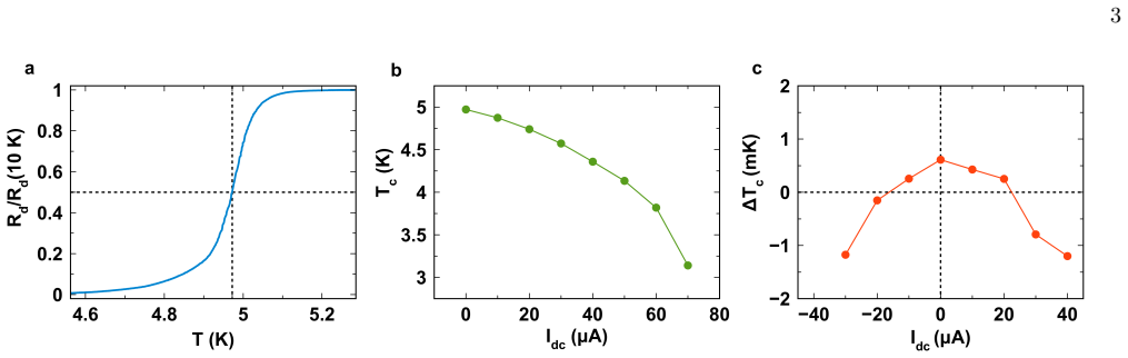
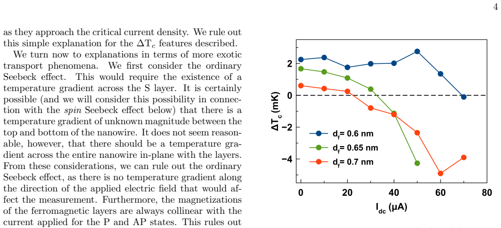
The central experimental discovery is a sign reversal of the spin-switch effect with bias current in Nb(20 nm)/Co(0.7 nm)/Cu(6 nm)/Co(2 nm)/CoOx(2 nm) nanowires. Measuring the differential-resistance midpoint as Tc, the authors find that ΔTc ≡ Tc(AP) − Tc(P) decreases monotonically with |Idc| and crosses zero near |Idc| = 20 μA. The same trend appears in devices with free-layer thicknesses from 0.6 to 0.7 nm. The authors argue that the reversal is produced by a spin Hall current in the niobium layer driven by the in-plane charge current: near Tc, Nb is a fluctuating mixture of normal and superconducting regions, so it both generates and transmits spin currents, and the resulting out-of-plane spin accumulation acts as a pair-breaking agent whose effect depends on the relative orientation of the two cobalt layers. Order-of-magnitude estimates of the spin current, using the known spin Hall angle of Nb, match the observed energy scale kBΔTc ≈ 2 × 10^−4 meV, and alternative mechanisms (ordinary Seebeck, anomalous Hall, Nernst, spin Seebeck, and simple current redistribution between layers) are ruled out qualitatively or quantitatively.
Load-bearing premise
The extraction of ΔTc assumes that the ±1 kOe field sweeps fully switch the free cobalt layer between well-defined parallel and antiparallel states at every bias current, and that the midpoint of the differential-resistance transition remains a faithful measure of Tc at finite bias.
Editorial extensions
If this is right
- In the operating range of cryogenic memory devices, the bias current itself can invert the sign of the spin-switch effect, so the magnetic state with higher Tc at zero bias becomes the lower-Tc state at finite bias.
- At non-zero bias, |ΔTc| can be enhanced relative to its zero-bias value, which may be exploited to strengthen the readout signal of a spin-valve memory element.
- The sign-reversal point provides a direct, calibration-free measure of the spin Hall current generated in the superconductor near Tc.
- The bias dependence must be considered in any S/F/N/F device design where sensing currents approach tens of microamps in nanowire-sized cross-sections.
Reading between the lines
- If the spin Hall mechanism is correct, replacing Nb with a superconductor of opposite spin Hall angle should reverse the direction of the ΔTc shift with bias, a testable prediction not made in the paper.
- The sign reversal could be used as a sensitive local probe of spin accumulation in superconducting devices: the crossing current measures the spin current density integrated over the wire cross-section.
- The same spin Hall picture suggests that the effect should scale with the nanowire width-to-thickness ratio; narrower or thicker wires should show the sign reversal at smaller or larger currents, which can be checked by systematic geometric sweeps.
Signed reviews
Editorial analysis
A structured set of objections, weighed in public.
Referee Report
Summary. The paper reports an experimental study of the spin switch effect (SSE) in Nb(20 nm)/Co(0.7 nm)/Cu(6 nm)/Co(2 nm)/CoOx(2 nm) nanowires patterned into Hall bars, in which the superconducting transition temperature Tc is measured as a function of direct bias current Idc for parallel (P) and antiparallel (AP) magnetic configurations. The central empirical claim is that ΔTc = Tc(AP) - Tc(P) decreases with increasing |Idc| and changes sign near |Idc| ≈ 20 μA, with a similar trend for devices with slightly different free-layer thicknesses. The paper attributes the behavior to a spin Hall current generated in Nb that flows perpendicular to the layers and suppresses Tc, and it argues against several alternative mechanisms on qualitative or quantitative grounds. The manuscript includes three data points per device family, no error bars, and no raw transition curves at finite bias; the theoretical interpretation is presented as a semi-quantitative plausibility argument.
Significance. If the sign-change of ΔTc with bias current is real, it is an interesting and potentially device-relevant nonequilibrium proximity effect: the magnetic configuration that is more superconducting at equilibrium becomes the less superconducting configuration at finite current. The paper has several strengths: the central quantity ΔTc is measured directly rather than inferred from a model, the measurements are repeated on three devices with different free-layer thicknesses, and the discussion explicitly eliminates several mundane mechanisms (ordinary Seebeck, anomalous Hall, Nernst, current redistribution) on stated grounds. The spin Hall interpretation is also framed as a consistency check rather than an ab initio prediction. However, the empirical claim is not yet established to the standard needed for publication: the sign change rests entirely on a single midpoint Tc-extraction criterion, no statistical or systematic uncertainty is reported, and possible current-induced magnetic-state and heating artifacts are not excluded experimentally.
major comments (4)
- [Section II, Fig. 2c] The central sign-change claim depends on defining Tc as the midpoint Rd(Tc)=Rd(10 K)/2 of the differential-resistance transition for P and AP states selected by alternating ±1 kOe during a slow temperature sweep at fixed Idc. The manuscript does not show any raw Rd(T) curves at finite bias, does not report an alternative Tc criterion (e.g., onset or 10%/90% points), and does not show high-bias GMR loops confirming that the free Co layer is fully and repeatedly switched between the same P and AP states at every current. Without such evidence, the observed ΔTc reversal could be a property of the extraction protocol rather than of the intrinsic pair-breaking in the two magnetic configurations.
- [Section II and Fig. 1c] Two specific artifacts are not experimentally excluded. First, Joule heating: because the P and AP states have different resistances (GMR ≈ 0.55% at 10 K, and the MR sign and magnitude can change near Tc), the I^2ΔR term makes the higher-resistance state locally warmer at Idc ≈ 20-40 μA, shifting its apparent transition to a lower cryostat temperature in exactly the direction of the observed reversal. Second, the Oersted field from 20 μA in a 200 nm wide wire is of order 200 Oe, comparable to the 0.2 kOe switching field of the free layer, so the alternating-field protocol may not prepare the same saturated configurations at every bias. The paper provides no control measurements (e.g., GMR loops at the bias currents used, or temperature-sweep data with reversed field history) to rule out either effect.
- [Section III, Eqs. (1)-(3)] The spin Hall interpretation is a consistency check, not a validation: the measured ΔTc is used to infer a required spin current via IS = kB ΔTc G Nch, with G assumed of order G0 and Nch left as a free parameter, and then Eq. (1) is used to ask whether the spin Hall effect can supply that current. The relation between a transverse spin current and the suppression of Tc is not derived from the proximity-effect theory used in the paper, and the assumed ΘSH for Nb ranges over an order of magnitude (10^-3 to 10^-2). As written, the estimate cannot discriminate the spin Hall mechanism from any mechanism that produces a comparable longitudinal spin current; a falsifiable prediction (e.g., a computed ΔTc(Idc) curve with fixed material parameters, or a measurement on a control sample with a different normal-metal layer) would be needed.
- [Figs. 2c and 3] The paper reports no error bars, no statement of measurement uncertainty, and no reproducibility information for the sign-change point. The zero-bias values and the bias-dependent trends are shown as single points for each device without indicating the scatter from repeated thermal cycles or from field-history repetitions. Given that the sign reversal is the main new result, the absence of any uncertainty estimate makes it impossible to assess whether the crossing near |Idc| = 20 μA is statistically significant.
minor comments (5)
- [Section III] The term 'transverse current' is used for a current flowing in the plane of the layers, which is transversely oriented with respect to the layer normal; this is the reverse of the usual convention in spin-Hall literature and is confusing. The authors should define the geometry explicitly with respect to both the layer normal and the nanowire axis.
- [Introduction and Fig. 1c] The text states that 'all samples exhibit conventional current-in-plane GMR' but only one device's GMR curve is shown in Fig. 1c; the GMR loops for the other two devices, and any device-to-device variation in the switching field, should be reported.
- [References] There are several presentation errors: in reference [30] the author name appears as 'C. Srgers' instead of 'C. Sürgers', and the paper uses both '0.55 %' and '0.55%' inconsistently. Also, the spin Hall angle reference [53] is for Nb but the text notes a competing value [54]; the authors should clarify which value is used for the central estimate.
- [Fig. 3] The figure caption does not state whether the three devices were co-fabricated on the same wafer or from different deposition runs, nor does it specify the measurement conditions (temperature sweep rate, field alternation sequence) for the data shown; this information is needed to judge the comparability of the three curves.
- [Section II] The temperature stability is quoted as 0.1 mK, but the reported ΔTc values and their bias dependence are not accompanied by a discussion of how the 2 mK/min sweep rate and the lock-in time constant affect the effective temperature resolution; this could be a minor source of systematic uncertainty in Tc extraction.
Circularity Check
No significant circularity: the central ΔTc(I) sign reversal is a direct measurement, and the spin Hall discussion is an explicitly semi-quantitative consistency check.
full rationale
The paper's central claim—that ΔTc ≡ Tc(AP)−Tc(P) decreases with |Idc| and changes sign near |Idc| ≈ 20 μA—is an experimental result extracted from measured differential-resistance transitions (Fig. 2c), not a quantity derived from a fitted parameter or from the authors' prior theory. The theoretical content in Section III is used retrospectively: the authors take the measured ΔTc, convert it to an energy scale kBΔTc ≈ 2×10^-4 meV, then ask what spin Hall current and channel count would be required to match it, finding Nch ≈ 5×10^6 to 5×10^8. This is a plausibility/consistency argument rather than a prediction, so it does not reduce the observation to the theory by construction. The self-citations to Refs. 42–46 support the qualitative premise that sharp P/AP conductance changes occur near a critical bias, but that premise is not used to generate the sign reversal, and no uniqueness theorem is invoked to forbid alternatives. Alternative mechanisms are excluded by independent order-of-magnitude estimates, not by circular appeal to self-citation. The midpoint definition of Tc and the ±1 kOe switching protocol could raise legitimate measurement-artifact concerns, but those concerns concern experimental correctness and robustness, not circular derivation. No fitted input is renamed as a prediction, and no equation reduces to another by definition. Therefore the paper is not circular in the sense under review.
Assumptions & free parameters
free parameters (1)
- Spin Hall angle of Nb (Theta_SH) =
~10^-3, with 10^-2 considered as upper estimate
assumptions (4)
- domain assumption Quasiclassical self-consistent theory of S/F proximity systems (Refs. 39-41) quantitatively describes equilibrium Delta-Tc in these samples.
- domain assumption Transport calculations for longitudinal (out-of-plane) current (Refs. 42, 44-46) provide relevant insight for the in-plane current data, at least semi-quantitatively.
- ad hoc to paper The relation between spin current and Tc suppression, IS = kB Delta-Tc G Nch, holds with G of order G0.
- domain assumption The free Co layer is fully switched between P and AP configurations by +/-1 kOe at all measured bias currents.
Cite this review
Pith. "Pith review of Bias current dependence of superconducting transition temperature in superconducting spin valve nanowires." pith.science (2026). https://pith.science/paper/IMJHZZFU
@misc{pith2026190803612,
  author       = {Pith},
  title        = {Pith review of: Bias current dependence of superconducting transition temperature in superconducting spin valve nanowires},
  year         = {2026},
  howpublished = {\url{https://pith.science/paper/IMJHZZFU}},
  note         = {Machine review of arXiv:1908.03612}
}
abstract
Competition between superconducting and ferromagnetic ordering at interfaces between ferromagnets (F) and superconductors (S) gives rise to several proximity effects such as odd-triplet superconductivity and spin-polarized supercurrents. A prominent example of an S/F proximity effect is the spin switch effect (SSE) observed in S/F/N/F superconducting spin-valve multilayers, in which the superconducting transition temperature T$_c$ is controlled by the angle $\phi$ between the magnetic moments of the F layers separated by a nonmagnetic metallic spacer N. Here we present an experimental study of SSE in Nb/Co/Cu/Co/CoO$_x$ nanowires measured as a function of bias current flowing in the plane of the layers. These measurements reveal an unexpected dependence of T$_c(\phi)$ on the bias current: T$_c(\pi)$--T$_c(0)$ changes sign with increasing current bias. We attribute the origin of this bias dependence of the SSE to a spin Hall current flowing perpendicular to the plane of the multilayer, which suppresses T$_c$ of the multilayer. The bias dependence of SSE can be important for hybrid F/S devices such as those used in cryogenic memory for superconducting computers as device dimensions are scaled down to the nanometer length scale.
Figures

Reference graph
Works this paper leans on
- [1]
-
[2]
N. Bergeal, F. Schackert, M. Metcalfe1, R. Vijay, V. E. Manucharyan, L. Frunzio, D. E. Prober, R. J. Schoelkopf, S. M. Girvin, and M. H. Devoret, Nature 465, 64 (2010)
work page 2010
-
[3]
H. Paik, D. I. Schuster, L. S. Bishop, G. Kirchmair, G. Catelani, A. P. Sears, B. R. Johnson, M. J. Reagor, L. Frunzio, L. I. Glazman, S. M. Girvin, M. H. Devoret, and R. J. Schoelkopf, Phys. Rev. Lett. 107, 240501 (2011)
work page 2011
- [4]
-
[5]
R. Barends, J. Kelly, A. Megrant, D. Sank, E. Jeffrey, Y. Chen, Y. Yin, B. Chiaro, J. Mutus, C. Neill, P. OMalley, P. Roushan, J. Wenner, T. C. White, A. N. Cleland, and J. M. Martinis, Phys. Rev. Lett. 111, 080502 (2013)
work page 2013
-
[6]
M. H. Devoret and R. J. Schoelkopf, Science 339, 1169 (2013)
2013
-
[7]
Krantz, M
P. Krantz, M. Kjaergaard, F. Yan, T. P. Orlando, S. Gus- tavsson, and W. D. Oliver, Appl. Phys. Rev. 6, 021318 (2019)
2019
-
[8]
V. K. Semenov, Y. A. Polyakov, and S. K. Tolpygo, IEEE Trans. Appl. Supercond. 29, 1302809 (2019)
work page 2019
Show all 58 references
-
[9]
D. S. Holmes, A. L. Ripple, and M. A. Manheimer, IEEE Trans. Appl. Supercond. 23, 1701610 (2013)
2013
-
[10]
M. A. Manheimer, IEEE Trans. Appl. Supercond. 25, 1301704 (2015)
2015
-
[11]
D. S. Holmes, A. M. Kadin, and M. W. Johnson, Com- puter 48, 34 (2015)
2015
-
[12]
T. I. Larkin, V. V. Bolginov, V. S. Stolyarov, V. V. Ryazanov, I. V. Vernik, S. K. Tolpygo, and O. A. Mukhanov, Appl. Phys. Lett. 100, 222601 (2012)
2012
-
[13]
F. S. Bergeret, A. F. Volkov, and K. B. Efetov, Phys. Rev. Lett. 86, 3140 (2001)
2001
-
[14]
Y. M. Blanter and F. W. J. Hekking, Phys. Rev. B 69, 024525 (2004)
2004
-
[15]
Linder and A
J. Linder and A. Sudbo, Phys. Rev. B 76, 064524 (2007)
2007
-
[16]
B. Baek, W. H. Rippard, M. R. Pufall, S. P. Benz, S. E. Russek, H. Rogalla, and P. D. Dresselhaus, Phys. Rev. Appl. 3, 011001 (2015)
2015
-
[17]
M. L. Schneider, C. A. Donnelly, S. E. Russek, B. Baek, M. R. Pufall, P. F. Hopkins, P. D. Dresselhaus, S. P. Benz, and W. H. Rippard, Sci. Adv. 4, e1701329 (2018)
2018
-
[18]
I. M. Dayton, T. Sage, E. C. Gingrich, M. G. Loving, T. F. Ambrose, N. P. Siwak, S. Keebaugh, C. Kirby, D. L. Miller, A. Y. Herr, Q. P. Herr, and O. Naaman, IEEE Magn. Lett. 9, 3301905 (2018)
2018
-
[19]
Dieny, V
B. Dieny, V. S. Speriosu, S. S. P. Parkin, B. A. Gurney, D. R. Wilhoit, and D. Mauri, Phys. Rev. B 43, 1297 (1991)
1991
-
[20]
J. Y. Gu, C.-Y. You, J. S. Jiang, J. Pearson, Ya. B. Bazaliy, and S. D. Bader, Phys. Rev. Lett. 89, 267001 (2002)
2002
-
[21]
Potenza and C
A. Potenza and C. H. Marrows, Phys. Rev. B 71, 180503(R) (2005)
2005
-
[22]
I. C. Moraru, W. P. Pratt, Jr., and N. O. Birge, Phys. Rev. Lett. 96, 037004 (2006)
2006
-
[23]
Miao, A.V
G.-X. Miao, A.V. Ramos, and J. S. Moodera, Phys. Rev. Lett. 101 137001 (2008)
2008
-
[24]
J. Zhu, X. Cheng, C. Boone, and I. N. Krivorotov, Phys. Rev. Lett. 103, 027004 (2009)
2009
-
[25]
Zhu, I.N
J. Zhu, I.N. Krivorotov, K. Halterman, and O. T. Valls, Phys. Rev. Lett. 105, 207002 (2010)
2010
-
[26]
A. A. Jara, C. Safranski, I. N. Krivorotov, C.-T. Wu, A. N. Malmi-Kakkada, O. T. Valls, and K. Halterman, Phys. Rev. B 89, 184502 (2014)
2014
-
[27]
A. Y. Rusanov, S. Habraken, and J. Aarts, Phys. Rev. B 73, 060505(R) (2006)
2006
-
[28]
Steiner and P
R. Steiner and P. Ziemann, Phys. Rev. B 74, 094504 (2006)
2006
-
[29]
Stamopoulos, E
D. Stamopoulos, E. Manios, and M. Pissas, Phys. Rev. B 75, 184504 (2007)
2007
-
[30]
Singh, C
A. Singh, C. Srgers, and R. Hoffmann, Appl. Phys. Lett. 91, 152504 (2007)
2007
-
[31]
P. V. Leksin, N. N. Garif’yanov, I. A. Garifullin, J. Schu- mann, H. Vinzelberg, V. Kataev, R. Klingeler, O. G. Schmidt, and B. B¨ uchner, Appl. Phys. Lett.97, 102505 (2010)
2010
-
[32]
P. V. Leksin, N. N. Garif’yanov, I. A. Garifullin, J. Schu- mann, V. Kataev, O. G. Schmidt, and B. B¨ uchner, Phys. Rev. Lett. 106, 067005 (2011)
2011
-
[33]
P. V. Leksin, N. N. Garif’yanov, I. A. Garifullin, J. Schu- mann, V. Kataev, O. G. Schmidt, and B. B¨ uchner, Phys. Rev. B 85, 024502 (2012)
2012
-
[34]
X. L. Wang, A. Di Bernardo, N. Banerjee, A. Wells, F. S. Bergeret, M. G. Blamire, and J. W. A. Robinson, Phys. Rev. B 89, 140508(R) (2014)
2014
-
[35]
H. G. Tompkins and J. A. Augis, Oxid. Met. 16, 355 (1981)
1981
-
[36]
Gredig, I
T. Gredig, I. N. Krivorotov, C. Merton, A. M. Goldman, and E. D. Dahlberg, J. Appl. Phys. 87, 6418 (2000)
2000
-
[37]
Gredig, I
T. Gredig, I. N. Krivorotov, and E. D. Dahlberg, J. Appl. Phys. 91, 7760 (2002)
2002
-
[38]
Eschrig, Phys
M. Eschrig, Phys. Today 64, 43 (2011)
2011
-
[39]
Halterman and O
K. Halterman and O. T. Valls, Phys. Rev. B 66, 224516 (2002)
2002
-
[40]
Halterman, P.H
K. Halterman, P.H. Barsic, and O. T. Valls, Phys. Rev. Lett. 99 127002 (2007)
2007
-
[41]
C.-T. Wu, O. T. Valls, and K. Halterman, Phys. Rev. Lett. 108, 117005 (2012)
2012
-
[42]
Moen and O
E. Moen and O. T. Valls, Phys. Rev. B 98 , 104512 (2018)
2018
-
[43]
Demler, G.B
E.A. Demler, G.B. Arnold, and M.R. Beasley, Phys. Rev. B55, 15174, (1997)
1997
-
[44]
C.-T. Wu, O. T. Valls, and K. Halterman, Phys. Rev. B 90, 054523 (2014)
2014
-
[45]
Moen and O
E. Moen and O. T. Valls, Phys. Rev. B95, 054503 (2017). 7
2017
-
[46]
Moen and O
E. Moen and O. T. Valls, Phys. Rev. B97, 174506 (2018)
2018
-
[47]
Takahashi and S
S. Takahashi and S. Maekawa, Jpn. J. Appl. Phys. 51, 010110 (2012)
2012
-
[48]
Espedal, P
C. Espedal, P. Lange, S. Sadjina, A. G. Mal’shukov, and A. Brataas, Phys. Rev. B 95, 054509 (2017)
2017
-
[49]
Derunova, Y
E. Derunova, Y. Sun, C. Felser, S. S. P. Parkin, B. Yan, and M. N. Ali, Sci. Adv. 5, eaav8575 (2019)
2019
-
[50]
Kontani, J
H. Kontani, J. Goryo, and D. S. Hirashima, Phys. Rev. Lett. 102, 086602 (2009)
2009
-
[51]
Wakamura, H
T. Wakamura, H. Akaike, Y. Omori, Y. Niimi, S. Taka- hashi, A. Fujimaki, S. Maekawa, and Y. Otani, Nature Mater. 14, 675 (2015)
2015
-
[52]
Taira, M
T. Taira, M. Ichioka, S. Takei, and H. Adachi, Phys. Rev. B 98, 214437 (2018)
2018
-
[53]
K.-R. Jeon, C. Ciccarelli, H. Kurebayashi, J. Wunderlich, L. F. Cohen, S. Komori, J. W. A. Robinson, and M. G. Blamire, Phys. Rev. Appl. 10, 014029 (2018)
2018
-
[54]
Morota, Y
M. Morota, Y. Niimi, K. Ohnishi, D. H. Wei, T. Tanaka, H. Kontani, T. Kimura, and Y. Otani, Phys. Rev. B 83, 174405 (2011)
2011
-
[55]
Uchida, S
K. Uchida, S. Takahashi, K. Harii, J. Ieda, W. Koshibae, K. Ando, S. Maekawa, and E. Saitoh, Nature 455, 778 (2008)
2008
-
[56]
Valenzuela and M
S. Valenzuela and M. Tinkham, Nature 442, 176 (2006)
2006
-
[57]
Saitoh, M
E. Saitoh, M. Ueda, H. Miyajima, and G. Tatara, Appl. Phys. Lett. 88, 182509 (2006)
2006
-
[58]
A. Sola, P. Bougiatioti, M. Kuepferling, D. Meier, G. Reiss, M. Pasquale, T. Kuschel, and V. Basso, Sci. Rep. 7, 46752 (2017)
2017
Reviewed August 14, 2026 · model on record in the stance chip above.
Discussion (0). Continue with ORCID to comment.