REVIEW 3 major objections 5 minor 48 references
Transport across a topoelectrical Weyl semimetal heterojunction
T0 review · 3 major / 5 minor · reviewed 2026-08-14 · deepseek-v4-flash
Pith's one-line read A capacitor-inductor network mimics a Weyl heterojunction and shows 'anti-Klein' tunneling: some valleys are totally blocked at normal incidence, the reverse of Klein tunneling.
desk verdict A useful circuit-platform proposal whose anti-Klein tunneling argument is clear and plausible, but whose quantitative 3D transmission results need to be written out before the claims are fully checkable. read the letter →
The pith
A machine-rendered reading of the paper's core claim, the machinery that carries it, and where it could break.
The reading
What carries the argument
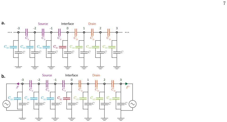
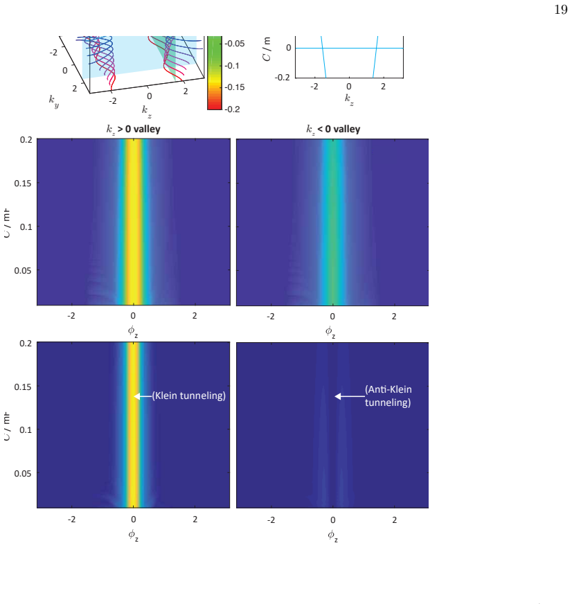
The machine that carries the argument is the topoelectrical analogue: a voltage node in an LC network maps to a tight-binding lattice site, a coupling capacitor maps to a hopping integral, the common grounding capacitance $C$ maps to the eigenenergy, and the energy flux $j_{E;n} = \frac{1}{\omega}\operatorname{Im}(C_{n+1;n}V_{n+1}^*V_n)$ maps to probability flux. The Type III phase is engineered by the condition $|C_{Az}+C_{Bz}| = |C_{Az}-C_{Bz}|$, which in the explicit model means $C_{Bz} = 0$; the Weyl cone then has one flat branch along the tilt direction, so the drain supports only one pseudospin species. The anti-Klein suppression follows from pseudospin orthogonality: at normal incidence the source mode from the negative-$k_z$ valley has $\langle\sigma_z\rangle = -1$ while every forward-propagating drain mode has $\langle\sigma_z\rangle = +1$, so the overlap vanishes. The transmission calculation is made finite and tractable by truncating the infinite leads to a few nodes with voltage supplies at the ends, justified through an analogy with lead self-energies.
What would settle it
Build or numerically simulate the paper's Type I–Type III junction with the stated parameters (e.g., $C_1 = 0.716$ mF, $C_y = 0.167$ mF, $C_{Az} = 0.5$ mF, $C_{Bz} = 0$) and measure or compute the transmitted energy flux at normal incidence for the negative-$k_z$ valley; the anti-Klein claim requires this transmission to be exactly zero. A decisive control is to add extra buffer nodes beyond the three used on each side of the interface — if the zero transmission shifts or becomes nonzero, the effect is an artifact of the finite-circuit truncation. A physical measurement only requires voltmeters on adjacent nodes plus the flux formula $j_{E;n}$, so the prediction is directly checkable.
Extended reading notes
Core claim
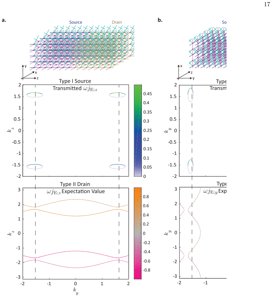
The central claim is that a three-dimensional LC circuit network hosts all three Weyl phases and computes their transport: writing Kirchhoff's current law at every node gives $C\mathbf{v} = H\mathbf{v}$, so the common grounding capacitance $C$ plays the role of eigenenergy, the node voltages play the wavefunction, and the conserved quantity $j_{E;n} = \frac{1}{\omega}\operatorname{Im}(C_{n+1;n}V_{n+1}^*V_n)$ is the analogue of probability flux. For a Type I source and Type II drain, the authors find that transmission is valley-independent when the tilt is perpendicular to the transport direction, and strongly valley-dependent when they are parallel, because the latter case requires large inter-valley momentum transfer. They identify a Type III phase at the Type I–II boundary, $|C_{Az}+C_{Bz}| = |C_{Az}-C_{Bz}|$, where one pseudospin branch has zero group velocity along the tilt direction and is flat in $k_z$. At a Type I–Type III junction, normally incident modes from the negative-$k_z$ valleys are completely blocked because the source and drain pseudospin states are orthogonal — the 'anti-Klein' tunneling that inverts the usual Klein result.
Load-bearing premise
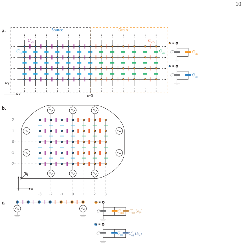
The load-bearing premise is that cutting the infinite or semi-infinite leads down to a small finite circuit — with voltage supplies at the ends supplying the missing currents — reproduces the transmission of the true infinite system; the paper argues this via a buffering argument in Section II.C (Eqs. 16–23) but does not prove the absence of spurious reflections from the finite boundaries.
Editorial extensions
If this is right
- A Type I–Type II heterojunction in a TE circuit is a tunable valley filter: transmission is valley-selective when transport is parallel to the tilt direction and valley-blind when perpendicular.
- The Type III phase should appear in a real circuit as a distinctive signature — equal-capacitance contours forming only two curves and a flat dispersion along the tilt direction — measurable with simple voltage probes.
- The anti-Klein zero at normal incidence gives a transport fingerprint that experimentally distinguishes a Type III drain from a Type II drain without band-structure measurements.
- Since the circuit is built from off-the-shelf capacitors and inductors, the entire predicted transmission map, including the anti-Klein suppression, is directly testable on a printed circuit board.
- The single-mode population achieved by setting terminal voltages isolates one incident channel, so the predicted valley-dependent transmission can be measured channel by channel, which is difficult in real Weyl materials.
Reading between the lines
- The same tilt-plus-flat-branch band structure exists in photonic and mechanical metamaterials, so the anti-Klein mechanism should transfer there; if it does, it is a generic feature of Type I–Type III interfaces rather than a circuit-specific quirk.
- A numerical stress test is cheap: recompute the transmission with four, five, or more buffer nodes on each side of the interface; if the normal-incidence zero moves or disappears, the finite-circuit truncation, not physics, produced the anti-Klein effect.
- A real conductance measurement would sum over all Fermi-surface channels, not a single mode; the authors' focus on one incident mode (at $k_x = \pi$) leaves open whether the anti-Klein suppression survives an angular average over the source Fermi surface.
- If the effect survives, a Type I–Type III junction is effectively a normally-off valve controlled by the valley polarization of injected modes, a possible element for valleytronic logic.
Signed reviews
Editorial analysis
A structured set of objections, weighed in public.
Referee Report
Summary. The manuscript develops a topoelectrical (TE) circuit realization of Weyl semimetal heterojunctions. It establishes an analogy between LC circuit KCL equations and tight-binding Hamiltonians, defines a conserved energy flux as the TE analogue of probability flux, and proposes a finite-circuit construction to model semi-infinite leads. Using a two-band lattice model with tunable tilt, it classifies Type I, II, and III WSM phases and computes transmission through Type I-Type II and Type I-Type III heterojunctions, reporting valley-dependent transmission, valley-independent transmission for perpendicular tilt/transport geometry, and a new 'anti-Klein' total suppression at normal incidence for Type III drains. The 1D and 2D mode-matching derivations are explicit; the 3D transmission calculations used for the main quantitative figures are only sketched.
Significance. If the results hold, the paper offers an experimentally practical platform for WSM heterojunction transport and identifies a qualitative effect, anti-Klein tunneling, that is distinct from conventional Klein tunneling. The strengths are the explicit derivation of the energy-flux analogue (Section II.E), the careful 1D buffering argument for replacing infinite leads by finite circuits (Section II.C), and the pseudospin-overlap argument at normal incidence (Section IV, Fig. 8), which makes the anti-Klein zero plausible and testable. However, the quantitative valley-dependent and valley-equal transmission claims in Figs. 6 and 7 rest on a 3D mode-matching calculation that is not presented, and the extension of the finite-circuit equivalence to 2D/3D is asserted rather than proved.
major comments (3)
- [Section IV (Figs. 6 and 7)] The transmitted energy flux is said to be calculated 'similar to what we did in Eqs. 21 to 23' (Section IV), but the 3D mode-matching equations are never written out. The paper does not provide the 3D KCL equations, the lead eigenmode expansions in all three dimensions, the interface boundary conditions, or an explicit definition of the transmission probability as a ratio of outgoing to incoming energy fluxes. Equations (26)-(27) contain only the two propagating ±κ modes, and no statement is made about whether evanescent modes are included in solving the interface problem. The quantitative results in Figs. 6 and 7, including the valley-independent transmission in Fig. 6b and the anti-Klein zeros in Fig. 7c, therefore cannot be checked by the reader. Please add the full mode-matching derivation for the WSM heterojunction, or a well-defined reduction of the 3D problem to effective 1D chains, with the transmission probability explicitly defined and normalized.
- [Section II.D] The buffering argument that a finite circuit with voltage supplies at the ends reproduces the transmission of the infinite system is explicitly demonstrated only for the one-dimensional chain in Section II.C. The extension to two and three dimensions is asserted by analogy, including the sufficiency of five transverse nodes and the selection of perimeter nodes with voltage supplies in Fig. 3b. Since the 3D transmission calculations of Section IV rely on the same equivalence, the paper should either prove the equivalence for multidimensional leads or provide a numerical convergence check showing that the computed fluxes are insensitive to the transverse/truncation buffer size. Without this, spurious reflections from the finite boundaries cannot be excluded.
- [Section IV and Abstract] The main results are stated without the kx=π caveat: the abstract says that for a Type I source and Type II drain all valleys transmit equally when tilt and transport are perpendicular, and the anti-Klein effect is described as a property of the heterojunction. However, Section IV states 'We therefore focus exclusively on the set of source modes with kx=π in the rest of the paper.' No argument is given that this restriction is without loss of generality for either the valley-equality claim or the anti-Klein suppression. The authors should either extend the calculation away from kx=π or explicitly qualify all conclusions as applying to the kx=π sector that the TE circuit can be prepared to excite.
minor comments (5)
- [Section II.C, Eqs. (18)-(19)] Equation (18) uses Ci in the second term on the right-hand side, where the source coupling capacitance CS should appear; Eq. (19) similarly appears to use Ci instead of CD. This looks like a transcription error.
- [Fig. 5 and Fig. 7] The Type II parameters are inconsistent: the main text gives CBz=0.2 mF, while the caption of Fig. 5 gives CBz=0.5 mF, and the caption of Fig. 7b refers to 'parameters in panel a' for a Type II drain, although panel a is the Type III case. Please reconcile these values and captions.
- [Section IV] The term 'anti-Klein tunneling' is potentially misleading, since the effect at normal incidence is a total reflection due to the absence of a propagating pseudospin-matched drain state rather than tunneling through a classically forbidden region; a short clarifying remark would help.
- [Section II.E, Eq. (38)] The phrase 'half the sum of ... and its complex conjugate' is a verbose way of saying the real part of the expression; the presentation could be simplified to improve readability.
- [Figs. 6 and 7] The color scales and some axis labels in Figs. 6 and 7 are not fully identified in the captions; making the units and the boundary between source and drain regions explicit would improve readability.
Circularity Check
No significant circularity: the anti-Klein suppression is derived from the model Hamiltonian and pseudospin overlap, not from fitted inputs or self-citation.
full rationale
The paper's central derivation is self-contained. It starts from KCL for an LC circuit, obtains the TE analogue C v = H v, and constructs the WSM Hamiltonian H(k) in Eq. 41 from the circuit topology. The phase classification in Eqs. 46-48 follows from expanding H around the Weyl points (Eq. 45), and the transmission is then obtained by mode matching with the conserved transverse momentum, as described after Eqs. 21-23. The anti-Klein zero at normal incidence is computed explicitly in Sec. IV: at δkx = δky = 0 and CBz = 0, Eq. 45 reduces to H = -CAz ηz δkz (I + σz), so the Type III drain has only the +σz branch, while normally incident source states from the negative kz valley have opposite pseudospin; orthogonality gives zero transmission. This is a consequence of the model, not an input. The circuit parameters (C1, Cy, CAz, CBz) are chosen, not fitted to any transmission data, and no fitted quantity is later renamed as a prediction. Self-citations to prior TE-circuit and WSM-transport work appear only as background and do not carry the derivation. The finite-circuit truncation argument in Sec. II.C is an explicit modeling assumption; even if it were incomplete in 3D, that is a verifiability/correctness concern, not a circular reduction.
Assumptions & free parameters
free parameters (3)
- Capacitance values C1, Cy, CAz for the WSM circuit =
C1=0.716 mF, Cy=0.167 mF, CAz=0.5 mF (chosen)
- Common grounding capacitance C =
C=0.1 mF in Figs. 6 and 8; scanned in Fig. 7
- Interface on-site capacitance C0I =
Not specified for the WSM heterojunction
assumptions (5)
- domain assumption KCL at circuit nodes yields an eigenvalue equation for the common grounding capacitance C, making C the analogue of the TB eigenenergy
- domain assumption A finite chain with voltage supplies at the ends models a semi-infinite lead, with the currents through the supplies acting as lead self-energies
- domain assumption The specific LC circuit of Fig. 4 hosts a Weyl semimetal Hamiltonian (Eq. 41) with four Weyl nodes
- standard math The reduction of higher-dimensional circuits to 1D via ky-dependent on-site terms is exact for eigenmodes
- ad hoc to paper Transmission can be restricted to source modes with kx=pi without loss of generality for the conclusions
invented entities (1)
-
Type III WSM phase
Cite this review
Pith. "Pith review of Transport across a topoelectrical Weyl semimetal heterojunction." pith.science (2026). https://pith.science/paper/EHTZ3KR2
@misc{pith2026190803642,
  author       = {Pith},
  title        = {Pith review of: Transport across a topoelectrical Weyl semimetal heterojunction},
  year         = {2026},
  howpublished = {\url{https://pith.science/paper/EHTZ3KR2}},
  note         = {Machine review of arXiv:1908.03642}
}
abstract
We propose a general method to realize and calculate the transmission in a Weyl semimetal (WSM) heterostructure by employing a periodic three-dimensional topoelectrical (TE) circuit network. By drawing the analogy between inductor-capacitor circuit lattices and quantum mechanical tight-binding (TB) models, we show that the energy flux in a TE network is analogous to the probability flux in a TB Hamiltonian. TE systems offer a key advantage in that they can be easily tuned to achieve different topological WSM phases simply by varying the capacitances and inductances. The above analogy opens the way to the study of tunneling across heterojunctions separating different types of WSMs in TE circuits, a situation which is virtually impossible to realize in physical WSM materials. We show that the energy flux transmission in a WSM heterostructure depends highly on the relative orientation of the transport direction and the $k$-space tilt direction. For the transmission from a Type I WSM source lead to a Type II WSM drain lead, all valleys transmit equally when the tilt and transmission directions are perpendicular to each other. In contrast, large inter-valley scattering is required for transmission when the tilt and transport directions are parallel to each other, leading to valley-dependent transmission. We describe a Type III WSM phase intermediate between the Type I and Type II phases. An `anti-Klein' tunneling occurs between a Type I source and Type III drain where the transmission is totally suppressed for some valleys at normal incidence. This is in direct contrast to the usual Klein tunneling in Dirac materials where normally incident flux is perfectly transmitted. Owing to the ease of fabrication and experimental accessibility, TE circuits offer an excellent testbed to study the extraordinary transport phenomena in WSM based heterostructures.
Figures

Figures from the paper (6 more)




Reference graph
Works this paper leans on
-
[1]
L. Lu, J. D. Joannopoulos and M. Solja c i\' c , Nat. Photonics 8, 821 (2014)
work page 2014
-
[2]
L. Lu, J. D. Joannopoulos and M. Solja c i\' c , Nat. Phys. 12, 626 (2016)
work page 2016
- [3]
-
[4]
D. Z. Rocklin et al., Phys. Rev. Lett 116, 135503 (2016)
work page 2016
-
[5]
X. Li, E. Zhao and W. V. Liu, Nat. Comm. 4, 1523 (2013)
work page 2013
- [6]
-
[7]
H. N. Krishnamoorthy et al., Science 336, 205 (2012)
work page 2012
- [8]
Show all 48 references
-
[9]
C. W. Peterson et al., Nat. 555, 346 (2018)
2018
-
[10]
Imhof et al., Nat
S. Imhof et al., Nat. Phys. 14, 925 (2018)
2018
-
[11]
C. H. Lee et al., Comm. Phys. 1, 39 (2018)
2018
-
[12]
Burkov and L
A. Burkov and L. Balents, Phys. Rev. Lett 107, 127205 (2011)
2011
-
[13]
Lv et al., Phys
B. Lv et al., Phys. Rev. X 5, 031013 (2015)
2015
-
[14]
Xu et al., Science 349, 613 (2015)
S.-Y. Xu et al., Science 349, 613 (2015)
2015
-
[15]
Li et al., Frontiers of Phys
Y. Li et al., Frontiers of Phys. 12, 127205 (2017)
2017
-
[16]
Huang et al., Phys
X. Huang et al., Phys. Rev. X 5, 031023 (2015)
2015
-
[17]
Wan et al., Phys
X. Wan et al., Phys. Rev. B 83, 205101 (2011)
2011
-
[18]
Xu et al., Science 347, 294 (2015)
S.-Y. Xu et al., Science 347, 294 (2015)
2015
-
[19]
Yesilyurt et al., Sci
C. Yesilyurt et al., Sci. Rep. 7, 4030 (2017)
2017
-
[20]
Yesilyurt et al., Sci
C. Yesilyurt et al., Sci. Rep. 6, 38862 (2016)
2016
-
[21]
O’Brien, M
T. O’Brien, M. Diez and C. Beenakker, Phys. Rev. Lett 116, 236401 (2016)
2016
-
[22]
S. A. Yang, H. Pan and F. Zhang, Phys. Rev. Lett 115, 156603 (2015)
2015
-
[23]
Yang, Y.-M
K.-Y. Yang, Y.-M. Lu and Y. Ran, Phys. Rev. B 84, 075129 (2011)
2011
-
[24]
Ezawa , Phys
M. Ezawa , Phys. Rev. B 87, 155415 (2013)
2013
-
[25]
Xu et al., Phys
G. Xu et al., Phys. Rev. Lett 107, 186806 (2011)
2011
-
[26]
Cortijo et al., Phys
A. Cortijo et al., Phys. Rev. B 94, 241405 (2016)
2016
-
[27]
Chang and M.-F
M.-C. Chang and M.-F. Yang, Phys. Rev. B 91, 115203 (2015)
2015
-
[28]
Burkov, Nat
A. Burkov, Nat. Mater. 15, 1145 (2016)
2016
-
[29]
Xu et al., (unpublished) arXiv:1604.02116 (2016)
N. Xu et al., (unpublished) arXiv:1604.02116 (2016)
2016 arXiv
-
[30]
Xu et al., Science advances 3, (2017)
S.-Y. Xu et al., Science advances 3, (2017)
2017
-
[31]
Yesilyurt et al., J
C. Yesilyurt et al., J. Appl. Phys. 112, 244303 (2017)
2017
-
[32]
Yesilyurt et al., Appl
C. Yesilyurt et al., Appl. Phys. Lett. 111, 063101 (2017)
2017
-
[33]
Yesilyurt et al., Sci
C. Yesilyurt et al., Sci. Rep. 9, 4480 (2019)
2019
-
[34]
A. A. Soluyanov et al., Nat. 527, 495 (2015)
2015
-
[35]
Deng et al., Nat
K. Deng et al., Nat. Phys. 12, 1105 (2016)
2016
-
[36]
Kumar et al., Nat
N. Kumar et al., Nat. Comm. 8, 1642 (2017)
2017
-
[37]
Jiang et al., Nat
J. Jiang et al., Nat. Comm. 8, 13973 (2017)
2017
-
[38]
Sharma, P
G. Sharma, P. Goswami and S. Tewari, Phys. Rev. B 96, 045112 (2017)
2017
-
[39]
Bialynicki-Birula, Phys
I. Bialynicki-Birula, Phys. Rev. D 49, 6920 (1994)
1994
-
[40]
Ezawa, Phys
M. Ezawa, Phys. Rev. B 98, 201402 (2018)
2018
-
[41]
K. Luo, R. Yu and H. Weng, Research 2018, 6793752 (2018)
2018
-
[42]
Ezawa, (unpublished) arXiv:1904.03823 (2019)
M. Ezawa, (unpublished) arXiv:1904.03823 (2019)
2019 arXiv
-
[43]
Helbig et al., Topological band structures in electric circuits
T. Helbig et al., Topological band structures in electric circuits. Bulletin of the American Phys. Society, 2019.CHANGE MANUALLY
2019
-
[44]
Ridolfi et al., J
E. Ridolfi et al., J. Phys.: Condens. Matter 27, 365501 (2015)
2015
-
[45]
Lu et al., Phys
Y. Lu et al., Phys. Rev. B 99, 020302 (2019)
2019
-
[46]
Helbig et al., Phys
T. Helbig et al., Phys. Rev. B 99, 161114 (2019)
2019
-
[47]
Datta, Quantum Transport: Atom to Transistor (Cambridge University Press, Cambridge, 2005), Chap
S. Datta, Quantum Transport: Atom to Transistor (Cambridge University Press, Cambridge, 2005), Chap. 9
2005
-
[48]
Datta and B
S. Datta and B. Das, App. Phys. Lett. 56, 665 (1990)
1990
Reviewed August 14, 2026 · model on record in the stance chip above.
Discussion (0). Continue with ORCID to comment.